- DL manuals
- Panasonic
- Plasma TV
- Viera TC-50PX24
- Service Manual
Panasonic Viera TC-50PX24 Service Manual
Summary of Viera TC-50PX24
Page 1
© panasonic corporation 2010. Unauthorized copying and distribution is a violation of law. Order no.Mtnc100320ce b34 canada: b62 50 inch class 720p plasma hdtv model no. Tc-p50x2 gph13du chassis.
Page 2: Table of Contents
2 table of contents page page 1 safety precautions -----------------------------------------------3 1.1. General guidelines ----------------------------------------3 2 warning --------------------------------------------------------------4 2.1. Prevention of electrostatic discharge (esd) to electros...
Page 3: 1 Safety Precautions
3 1 safety precautions 1.1. General guidelines 1. When conducting repairs and servicing, do not attempt to modify the equipment, its parts or its materials. 2. When wiring units (with cables, flexible cables or lead wires) are supplied as repair parts and only one wire or some of the wires have been...
Page 4: 2 Warning
4 2 warning 2.1. Prevention of electrostatic discharge (esd) to electrostatically sensitive (es) devices some semiconductor (solid state) devices can be damaged easily by static electricity. Such components commonly are called elec- trostatically sensitive (es) devices. Examples of typical es device...
Page 5
5 2.2. About lead free solder (pbf) note: lead is listed as (pb) in the periodic table of elements. In the information below, pb will refer to lead solder, and pbf will refer to lead free solder. The lead free solder used in our manufacturing process and discussed below is (sn+ag+cu). That is tin (s...
Page 6: 3 Service Navigation
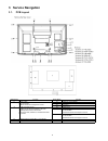
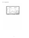
6 3 service navigation 3.1. Pcb layout board name function board name function p power supply non serviceable. P-board should be exchanged for service. C1 data driver (lower right) c2 data driver (lower left) sc scan drive a dc-dc converter, tuner speaker out, av terminal, hdmi in, sd card digital s...
Page 7
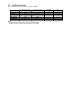
7 3.2. Applicable signals * mark: applicable input signal for component (y, pb, pr) and hdmi note • signals other than those shown above may not be displayed properly. • the above signals are reformatted for optimal viewing on your display. Horizontal frequency (khz) vertical frequency (hz) componen...
Page 8: 4 Specifications
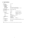
8 4 specifications power source ac 120 v, 60 hz power consumption maximum 299 w standby condition 0.3 w plasma display panel drive method ac type aspect ratio 16:9 visible screen size 50 inch class (49.9 inches measured diagonally) (w × h × diagonal) 43.5 inch × 24.4 inch × 49.9 inch (1,105 mm × 622...
Page 9: 5 Service Mode
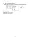
9 5 service mode 5.1. How to enter into service mode while pressing [volume ( - )] button of the main unit, press [info] button of the remote control three times within 2 seconds. 5.1.1. Key command [1] button...Main items selection in forward direction [2] button...Main items selection in reverse d...
Page 10
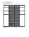
10 5.1.2. Contents of adjustment mode • value is shown as a hexadecimal number. • preset value differs depending on models. • after entering the adjustment mode, take note of the value in each item before starting adjustment. 5.1.3. How to exit switch off the power with the [power] button on the mai...
Page 11
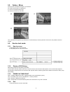
11 5.2. Option - mirror picture can be reversed left and right or up and down. 00 : default (normal picture is displayed) 01 : picture is reversed left and right. 02 : picture is reversed up and down. Hint : if the defective symptom (e.G. Vertical bar or horizontal bar) is moved by selection of this...
Page 12
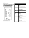
12 5.4. Hotel mode 1. Purpose restrict a function for hotels. 2. Access command to the hotel mode setup menu in order to display the hotel mode setup menu, please enter the following command (within 2 second). [tv] : vol. [down] + [remote] : input (3 times) then, the hotel mode setup menu is display...
Page 13
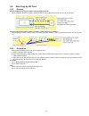
13 5.5. Data copy by sd card 5.5.1. Purpose (a) board replacement (copy the data when exchanging a-board): when exchanging a-board, the data in original a-board can be copied to sd card and then copy to new a-board. (b) hotel (copy the data when installing a number of units in hotel or any facility)...
Page 14
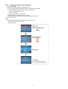
14 5.5.3. Data copy from tv set to sd card 1. Turn on the tv set. 2. Insert sd card with a startup file (pwd file) to sd slot. On-screen display will be appeared according to the startup file automatically. 3. Input a following password for (a) or (b) by using remote control. (a) for board replaceme...
Page 15
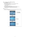
15 5.5.4. Data copy from to sd card to tv set 1. Turn on the tv set. 2. Insert sd card with data to sd slot. On-screen display will be appeared according to the data folder automatically. 3. Input a following password for (a) or (b) by using remote control. (a) for board replacement : 2771 (b) for h...
Page 16: 6 Troubleshooting Guide
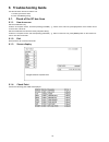
16 6 troubleshooting guide use the self-check function to test the unit. 1. Checking the iic bus lines 2. Power led blinking timing 6.1. Check of the iic bus lines 6.1.1. How to access self-check indication only: produce tv reception screen, and while pressing [volume ( - )] button on the main unit,...
Page 17
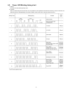
17 6.2. Power led blinking timing chart 1. Subject information of led flashing timing chart. 2. Contents when an abnormality has occurred the unit, the protection circuit operates and reset to the stand by mode. At this time, the defective block can be identified by the number of blinks of the power...
Page 18
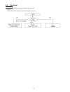
18 6.3. No power first check point there are following 2 states of no power indication by power led. 1. No lit 2. Red is lit then turns red blinking a few seconds later. (see 6.2.).
Page 19
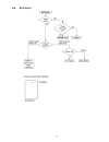
19 6.4. No picture.
Page 20
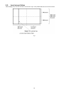
20 6.5. Local screen failure plasma display may have local area failure on the screen. Fig-1 is the possible defect p.C.B. For each local area. Fig-1.
Page 21: 7 Service Fixture & Tools
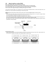
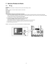
21 7 service fixture & tools 7.1. Sc jig purpose: to find the failure board (sc or su/sd) when the power led is blinking 7 times. Sc jig: jumper connector to connect to sc50 connector on sc board part number: tzsc09187 how to use: caution: remove sc jig from sc board after inspection. 1. Remove all ...
Page 22
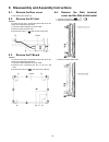
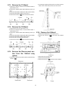
22 8 disassembly and assembly instructions 8.1. Remove the rear cover 1. See pcb layout (section 3) 8.2. Remove the ac inlet caution: to remove p.C.B. Wait 1 minute after power was off for dis- charge from electrolysis capacitors. 1. Unlock the cable clampers to free the cable. 2. Disconnect the con...
Page 23
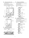
23 8.5. Remove the tuner unit 1. Remove the side terminal cover and the side shield metal. (see section 8.4.) 2. Unlock the cable clampers to free the cable. 3. Disconnect the connectors (a1, a6, a7 and a11). 4. Disconnect the flexible cables (a21, a33 and a34). 5. Remove the screws ( ×2 ) and remov...
Page 24
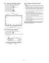
24 8.10. Remove the sc-board 1. Remove the su-board and sd-board. (see section 8.8. And 8.9.) 2. Unlock the cable clampers to free the cable. 3. Disconnect the connectors (sc2 and sc3). 4. Disconnect the flexible cable (sc20). 5. Remove the screws ( ×8 ) and remove the sc-board. 8.11. Remove the ss-...
Page 25
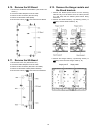
25 8.13. Remove the c1-board 1. Remove the hanger metal r and the stand bracket r. (see section 8.12.) 2. Remove the flexible cables holder fastening screws ( ×8 ). 3. Disconnect the flexible cables (cb1, cb2, cb3 and cb4). 4. Disconnect the flexible cables (c10 and c11). 5. Remove the screws ( ×4 )...
Page 26
26 8.17. Remove the glass holders 1. Remove the cabinet assy. (see section 8.15.) 2. Remove the s-board. (see section 8.16.) 3. Remove the screws ( ×4 ). 4. Remove the glass holder side (l, r). 5. Remove the screws ( ×9 ). 6. Remove the glass holder top. 7. Remove the screws ( ×7 ). 8. Remove the gl...
Page 27
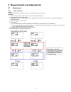
27 9 measurements and adjustments 9.1. Adjustment 9.1.1. Vsus selection caution: when plasma panel or a-board is replaced, vsus should be set to low or high. Procedure 1. Go into main item [vsus] in service mode. Low or high will be displayed. 2. Press [ok] button to go to test stage. White pattern ...
Page 28
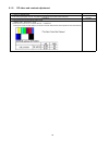
28 9.1.2. Rf video sub contrast adjustment name of measuring instrument remarks 1. Remote transmitter 2. Rf analog signal (sprit color bar. The pattern for adjustment must contain 100% white part.) procedure remarks 1. Receive the sprit color bar with rf analog signal. (aspect full, picture menu: vi...
Page 29
29 9.1.3. White balance adjustment name of measuring instrument remarks color analyzer (minolta ca-100 or equivalent) note: the ca-100 which was calibrated to less than +-0.001 with cs-1000. Procedure remarks • make sure the front panel to be used on the final set is fitted. • make sure a color sign...
Page 30
30
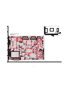
Page 31
31.
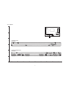
Page 32
32.
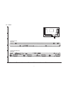
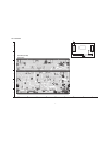
Page 33
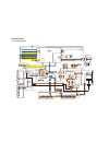
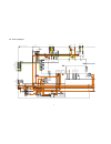
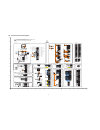
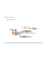
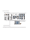
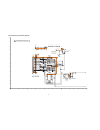
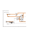
33 10 block diagram 10.1. Main block diagram (led:8time) (led:4time) (led:7times) cold hot (led:6times) (led:7times) (led:6times) (led:8times) (led:3times) (led:10times) (led:4times) (led:2times) (led:5times) data driver sc-board energy recovery sos detect data driver main sw1 c25 data driver c21 sc...
Page 34
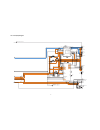
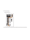
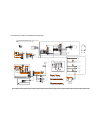
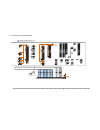
34 10.2. Block (1/4) diagram (led:10times) p q4703 d5605 d5604 sub3.3v vj5500 sub3.3v stb1.2v q5612 sub1.2v stb3.3v f15v q4704 p+15v sub5v q5613 stb5v stb3.3v sub1.8v d5629 f15v sub5v sub5v sound15v sub1.8v sub3.3v_sd sub3.3v sub3.3v p+15v d5603 stb5v q5605 stb5v sound15v stb3.3v x8000 sub5v q4702 p...
Page 35
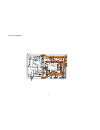
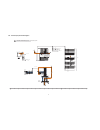
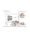
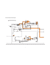
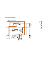
35 10.3. Block (2/4) diagram (led:7times) (led:8times) (led:2times) (led:3times) (led:4times) (led:5times) (led:6times) stb_d3.3v p+15v x9300 d2520 p+15v sub3.3v p+3.3v p+3.3v p+5v p+1.2v p+3.3v stb5v sub3.3v p+15v p+15v x9000 stb5v p+5v stb3.3v p+5v stb3.3v iic3 ic9001 2 vol.Dn for factory use pane...
Page 36
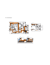
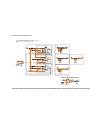
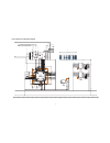
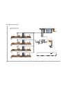
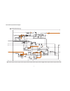
36 10.4. Block (3/4) diagram hot cold hot cold (led:4times) + + + + d151 f001 f002 d007 d008 d517 d521 d528 d525 d524 d017 d883 l005 d812 d811 d006 d010 d107 d106 d194 d193 d371 d551 d451 d491 l401 d602 d753 d607 d603 d615 vsus t101 p+15v pc803 ic101 1 p2 d001 +15v stb5v rectifier q608 p9 stb_5v_on ...
Page 37
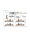
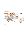
37 10.5. Block (4/4) diagram (led:8times) (led:6times) (led:7times) tpvsus tpss1 d16280 d16282 tpsos6 d16822 d16901 tpsc1 d16920 d16721 tpvad d16728 tpvsus tpvscn d16473 d16820 d16583 d16475 d16493 d16480 d16490 d16618 tpsos7 d16821 l16303 tpve 2 ic14901-04 driver scan sd 42b 4 su 11 scan driver ic1...
Page 38
38.
Page 39
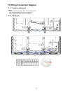
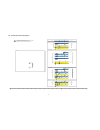
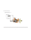
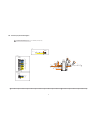
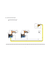
39 11 wiring connection diagram 11.1. Caution statement. Caution: please confirm that all flexible cables are assembled correctly. Also make sure that they are locked in the connectors. Verify by giving the flexible cables a very slight pull. 11.2. Wiring (1).
Page 40
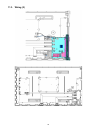
40 11.3. Wiring (2).
Page 41
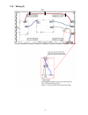
41 11.4. Wiring (3).
Page 42
42.
Page 43
43 12 schematic diagram 12.1. Schematic diagram note.
Page 44
44 12.2. A-board (1/14) schematic diagram s s s s s s s s p 0v 0v hdmi_cec c8082 10u 10v c8012 16v 0.1u c8020 16v 0.1u c8023 50v 5p c8001 6.3v 1u c8015 16v 150p c8002 6.3v 1u c8028 16v 0.1u c8019 16v 0.1u c8018 16v 0.1u c8017 16v 0.1u c8016 16v 0.1u c8014 16v 0.1u c8027 16v 0.1u c8011 16v 0.1u c8026...
Page 45
45 12.3. A-board (2/14) schematic diagram ch0a4 ch0xba2 ch0a5 ch0dq1 ch0dq2 ch0dq3 ch0dq14 ch0dq10 ch0dq6 ch0dq5 ch0dq12 ch0dq11 ch0dq4 ch0dq9 ch0dq0 ch0dq8 ch0dm0 ch0dqs0 ch0dq7 ch0dq13 ch0dq15 ch0dqs1 ch0dm1 ch0xcas ch0xcs0 ch0dqs1_n ch0dqs0_n 0v ch0cke ch0odt ch0a7 ch0a12 ch0a3 ch0a9 ch0a11 ch0a8...
Page 46
46 12.4. A-board (3/14) schematic diagram + s s s d.Sw w.P. Aa_ed1 aa_ea6 aa_ed4 aa_ed13 aa_ea3 aa_ea10 aa_ea21 aa_ea17 aa_xere ae_sdclk aa_ed2 aa_xecs0 aa_ed11 aa_ea8 aa_ed15 aa_ea18 aa_ea16 aa_ed14 aa_ea5 aa_ed8 aa_ea13 aa_ea2 aa_ea22 aa_ea11 aa_ea9 aa_xewe0 aa_xecs0 aa_ed12 aa_ed5 aa_ea14 aa_ed10...
Page 47
47 12.5. A-board (4/14) schematic diagram + thermal pad thermal pad thermal pad s p p p p p key3 c5667 25v 0.01u c5652 50v 1000p c5663 10v 10u c5765 1u 10v c5764 1u 10v c5703 1u 10v c5702 1u 10v c5771 0.033u 25v c5696 0.01u 16v c5698 22u 6.3v c5709 22u 6.3v c5713 0.1u 25v c5717 22u 6.3v c5722 10u 25...
Page 48
48 12.6. A-board (5/14) schematic diagram s s s s s s s s s s s s rf_v c2210 2.2u 10v c2199 10v 1u c2198 10v 1u c2213 10v 1u c2200 10v 1u c2201 10v 1u c2202 10v 1u c2204 10v 1u c2214 10v 1u c2103 10v 1u c2209 2.2u 10v c2208 2.2u 10v c2207 2.2u 10v c2297 2.2u 10v c2296 2.2u 10v c2212 2.2u 10v c2211 2...
Page 49
49 12.7. A-board (6/14) schematic diagram thermal pad s s p sdin_post lrclk_post audio_xrst 24kec_i2cdata1 24kec_i2cclk1 audio_xrst amp_mute sdin_post lrclk_post mclk_post bclk_post 24kec_i2cdata1 24kec_i2cclk1 amp_mute mclk_post bclk_post c2264 25v 0.1u c2234 25v 0.1u c2220 0.1u 16v c2250 50v 0.1u ...
Page 50
50 12.8. A-board (7/14) schematic diagram to 5/14 drive ic vcc vin gnd shield shield v r l r1 r2 l1 l2 pr1 pb2 l r y2 v pr2 pb1 y1 s ag_fan_sos c2283 0.1u 16v d2142 k7aaay000006 jk2111 k4ak08b00005 v v-g l l-g r r-g jk2103 k2ha918a0002 y1 y2 v g pb1 pb2 l g pr1 pr2 r g l1 l2 g r1 r2 g sub3.3v spdif ...
Page 51
51 12.9. A-board (8/14) schematic diagram hdmi_cec c4547 10v 1u c4546 10v 1u c4540 10v 1u c4541 10v 1u d4510 ezaeg2a50ax d4503 ezaeg2a50ax d4511 ezaeg2a50ax d4507 ezaeg2a50ax l4513 j0jyc0000068 l4500 j0jyc0000068 l4511 j0jyc0000068 l4502 j0jyc0000068 l4504 j0jyc0000068 l4512 j0jyc0000068 l4508 j0jyc...
Page 52
52 12.10. A-board (9/14) schematic diagram + s s s s s s s s p p p p if_monitor 21 rf_v rf_v 0v video_out rf_aft ag_rf_aft tu_sif fa_if_agc video_out tu_sif ag_rf_aft c8343 16v 0.1u c8318 50v 220p c8342 16v 0.1u c8328 16v 0.1u c8335 50v 220p c8339 50v 68p c8333 50v 150p c8334 50v 220p c8336 50v 39p ...
Page 53
53 12.11. A-board (10/14), k-board and s-board schematic diagram s p push vcc gnd out bottom pad nc ar_panel_sda d_iic_cont d_rxd ar_panel_sda ar_panel_scl d_iic_cont 24kec_i2cclk2 24kec_i2cdata2 mcu_i2cdata mcu_i2cclk ar_panel_scl d_txd 24kec_i2cdata1 24kec_i2cclk1 ar_stb_scl03 d_rxd d_txd ar_stb_s...
Page 54
54 12.12. A-board (11/14) schematic diagram (fin) term side s s p p stb_sda02 sos8_ss 24kec_i2cdata1 24kec_i2cclk1 sc_uhz p3v_sda02 p_on/off sos6 sos7 sos8 iic_sw sos6_sc1 stb_scl02 sos7_sc2 sos6_sc1 sos7_sc2 sc_uhz sc_crc1 sc_cel sc_cml sc_csl sc_sel2 sc_cph1 sc_csh sc_oc1 sc_cmh scnrst sc_crc2 sc_...
Page 55
55 12.13. A-board (12/14) schematic diagram s s s s s s s s rxd_pc sos8 sos7 osd_vin ar_panel_scl nrst ar_panel_scl d_rxd osd_cki osd_hi iic_cont rxd_pc 0v osd_b osd_hin stb_sda02 stb_scl02 panel_main_on sout iic_sw iic_cont txd_pc stb_scl01 panel_alarm/panel_led_on sclk ncs osd_r osd_g d_iic_cont d...
Page 56
56 12.14. A-board (13/14) schematic diagram to c1-board (c11) term side s s s s s s s s s s s s s p p osd_vin rclk_e+ rclk_o- rclk_e- p3v_scl02 rc_o+ p3v_sda02 rb_e+ osd_hin rc_e- d-pcd3 rb_o+ rb_e- rc_o- rd_o+ osd_b rd_e+ osd_hi rclk_o+ rc_e+ osd_cki d-oded2 rd_o- d-pcd2 d-oded1 d-pcd1 ueh_c ush_c ...
Page 57
57 12.15. A-board (14/14) schematic diagram term side p p p p p p sos8_ss drvrst dd9_2n dd9_2p dd12_1p dd12_1n dd12_2n drvclk7p drvclk7n dd11_2p dd11_2n dd10_1p dd10_1n dd10_2p drvclk6p drvclk6n dd9_1n d-led2 d-oded2 d-pcd3 d-pcd4 d-clrd2 umh_c ush_c usl/uml2_c ueh_c uml_c dd9_1p dd10_2n dd11_1p dd1...
Page 58
58 12.16. C1-board schematic diagram side term term side term side term side term side term side dd8_1- dd6_2- ab_clrd1 dd8_2+ drvclk3+ ab_pcd2 ab_oded1 dd8_2- drvclk3- ab_clrd1 drvclk4+ dd5_1+ ab_pcd2 ab_oded1 drvclk4- dd5_1- ab_led1 ab_clrd1 dd7_1+ dd5_2+ ab_pcd1 ab_oded1 dd7_1- dd5_2- ab_led1 ab_...
Page 59
59 12.17. C2-board schematic diagram side term term side term side term side term side term side drvclk6+ dd10_1- dd10_1+ drvclk7- drvclk6- dd12_1+ drvclk7- dd12_2+ ab_pcd3 drvclk7+ ab_led2 dd10_2+ ab_pcd4 ab_oded2 ab_oded2 ab_oded2 dd11_1+ dd11_1- dd10_2- drvclk7+ ab_led2 ab_clrd2 ab_clrd2 ab_clrd2...
Page 60
60 12.18. Sc-board (1/4) schematic diagram + + term side aa_csl aa_csh aa_oc1 main_stop0 aa_cml2 aa_sc_fpganrst aa_oc2 aa_cers aa_clk aa_siu aa_cis aa_uhz aa_cmh aa_cml aa_cel aa_cph1 aa_crc2 aa_crc1 mid c16593 50v 1000p c16562 16v 1u c16581 25v 1u c16566 50v 0.01u c16565 50v 0.01u c16564 16v 1u c16...
Page 61
61 12.19. Sc-board (2/4) schematic diagram sc-board txnsc1lnuu (2/4) to ss-board (ss3) + + + aa_csl aa_cml2 aa_cml aa_csh aa_cmh c16471 630v 1000p c16421 630v 5600p c16491 630v 1000p c16501 25v 1u c16771 16v 1u c16401 5600p 630v c16505 25v 1u c16521 25v 1u c16502 25v 4.7u c16504 25v 4.7u c16527 25v ...
Page 62
62 12.20. Sc-board (3/4) schematic diagram + aa_cis aa_cph1 aa_cel aa_crc1 aa_cers aa_crc2 vad vfg c16603 630v 1000p c16891 25v 1u c16664 50v 68p c16685 50v 0.1u c16684 50v 0.1u c16641 3300p 630v c16604 630v 1000p c16707 50v 22p c16665 50v 68p c16642 3300p 630v c16708 50v 0.1u c16602 50v 22p c16666 ...
Page 63
63 12.21. Sc-board (4/4) schematic diagram sc-board txnsc1lnuu (4/4) to su-board (su41b) to sd-board (sd46b) to sd-board (sd42b) for factory use + + + + + + + aa_sc_fpganrst main_stop0 aa_oc1 aa_clk aa_oc2 aa_siu aa_uhz c16863 50v 0.1u c16861 0.1u 16v c16472 25v 1u c16460 630v 2200p c16862 1u 10v c1...
Page 64
64 12.22. Ss-board (1/2) schematic diagram + + + aa_umh aa_sos8 aa_umh aa_uml aa_uml aaa_ueh c16001 630v 1000p c16131 25v 4.7u c16242 16v 1u c16135 25v 1u c16133 25v 4.7u c16018 1.5u 250v c16243 50v 0.01u c16022 630v 1000p c16103 25v 47p c16104 25v 47p c16244 10v 10u c16105 630v 220p c16106 630v 220...
Page 65
65 12.23. Ss-board (2/2) schematic diagram + + term side term side + aa_sos8 aaa_ueh aa_uml c16195 25v 1u c16317 1u 10v c16102 5600p 630v c16315 1u 10v c16192 25v 0.1u c16319 50v 0.1u c16318 0.1u 50v c16191 25v 4.7u c16316 0.1u 16v c16287 0.1u 50v c16286 0.1u 50v c16193 25v 47u c16328 200u 200v d163...
Page 66
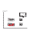
66 13 printed circuit board 13.1. K and s-board a b c d e f g h i 1 2 3 4 5 6 s 2 sw2500 pb f order no. 1 2 1 s tnpa4873 s 2 s w 2 5 0 0 s e e r e v e r s e f o r o r d e r n o . 1 2 p b f 1 s tnpa4873 c12 q 1 0 c 1 5 q 1 1 c 1 6 c 2 0 c21 c22 c 2 3 c 2 4 d12 r 1 6 r17 d20 d 2 4 r 2 0 r 2 4 r 2 5 r ...
Page 67
67 13.2. A-board a b c d e f g h i 1 2 3 4 5 6 ic9001 ic9004 ic5604 ic8502 q4703 j k 2 1 1 1 ic9400 ic9401 ic9402 za4700 i c 9 8 0 2 ic9804 ic2105 q 8 3 0 1 q8302 q8303 q 8 3 0 4 q8305 q 8 3 0 6 q 8 3 0 7 q8308 d2142 tu8302 i c 8 5 0 3 q4502 q4702 i c 9 3 0 4 q4704 q4512 ic4700 q8005 i c 9 1 8 9 ic8...
Page 68
68 a b c d e f g h i 1 2 3 4 5 6 s w 3 7 6 3 a a30 a37 ic9003 za4701 i c 9 8 0 0 ic9803 a7 q 5 6 0 0 c n 8 5 0 0 q 5 6 1 0 q5611 s w 3 7 6 5 a q5612 q 5 6 1 3 s w 3 7 6 4 a i c 5 6 0 5 ic5606 ic5608 i c 5 6 1 0 ic5613 q 9 0 0 2 q 9 0 0 4 thermal pad t h e r m a l p a d c h d n v o l u p c h u p ther...
Page 69
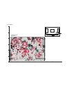
69 13.3. C1-board a b c d e f g h i 1 2 3 4 5 6 c 1 0 4 c 1 0 5 c 1 0 6 c 1 0 7 c 1 0 8 c 1 0 9 i c 1 0 1 c 1 1 0 c 1 1 1 c 1 1 2 c113 c 1 1 4 c 1 1 5 c 1 1 6 c117 c 1 1 8 c119 c 1 2 0 c 1 2 1 c 1 2 2 fl102 za102 za103 za104 za105 r 1 0 1 r 1 0 2 r 1 0 3 r 1 0 4 r 1 0 5 r 1 0 6 r 1 0 7 r 1 0 8 r 1 0...
Page 70
70 13.4. C2-board a b c d e f g h i 1 2 3 4 5 6 c20 c21 c23 c25 c 2 0 4 c205 c 2 0 6 c 2 0 7 c208 cb5 c 2 0 9 i c 2 0 2 cb6 i c 2 0 3 cb7 cb8 c 2 1 0 c211 c212 c213 c 2 1 4 c215 c 2 1 6 c217 c218 c 2 1 9 c220 c221 c222 c223 c224 c 2 2 5 c 2 2 6 c 2 2 7 c228 c 2 2 9 f l 2 0 1 c 2 3 0 za201 za202 za20...
Page 71
71 13.5. Sc-board a b c d e f g h i 1 2 3 4 5 6 sc41 sc42 t p 9 0 t p 9 1 t p 9 2 sc46 t p 9 3 t p 9 4 tp95 t p 9 6 t p 9 9 l698 sc50 c563 d 7 2 2 d724 t p 1 0 0 t p 1 0 5 t p 1 0 6 tp107 tp108 t471 t p 1 0 9 ic784 ic786 t p 1 1 0 tp111 c791 tp112 c793 t p 1 1 3 t p 1 1 4 c795 t p 1 1 5 c796 t p 1 1...
Page 72
72 a b c d e f g h i 1 2 3 4 5 6 sc41 q 7 0 1 q 7 0 2 sc42 d 5 0 3 sc46 d 7 0 1 d 7 0 2 l 6 9 8 sc50 c753 c 7 5 4 q 5 2 1 c 7 5 5 c561 c756 c 5 6 2 c757 c 5 6 3 c 5 6 4 d 9 0 1 c 5 6 5 c566 d710 d 7 1 1 ic561 ic562 d 7 1 2 d713 ic563 d 5 2 2 q 5 3 1 d 7 1 9 d 7 2 0 q 9 2 0 q 9 2 1 d 7 2 1 d 7 2 2 d ...
Page 73
73 13.6. Ss-board a b c d e f g h i 1 2 3 4 5 6 c 1 9 3 ss11 r309 l 1 0 3 l 3 0 3 s s 5 2 s s 5 5 ss3 c003 c011 c012 c018 c023 c 2 4 1 c272 tpvsus tp2 tp7 tp8 l 0 1 1 l 0 1 2 l 0 1 3 l 0 1 4 tp13 tp14 tp16 tp17 tp18 tpsos8 tp24 tp25 tp26 tp27 tp28 tp29 c105 s s 5 3 a s s 5 3 b c106 tp30 tp31 tp32 tp...
Page 74
74 a b c d e f g h i 1 2 3 4 5 6 d 3 1 5 d 3 1 6 d317 d 1 3 1 q 1 4 1 r 1 0 1 r102 r 1 0 3 r104 c 1 9 1 r 1 0 5 c 1 9 2 c 1 9 3 ss11 r109 c195 c198 r 1 1 0 r 3 0 7 r309 q 1 6 1 r 1 1 6 ss23 r 3 1 8 r319 r 3 2 0 za001 za002 l 1 0 3 r 1 3 1 r 1 3 2 r 1 3 4 r 1 3 5 r 1 3 6 r 1 3 7 l 3 0 3 r 3 3 0 ic241...
Page 75
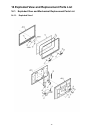
75 14 exploded view and replacement parts list 14.1. Exploded view and mechanical replacement parts list 14.1.1. Exploded view 1.
Page 76
76 14.1.2. Exploded view 2.
Page 77
77 14.1.3. Accessories.
Page 78
78 14.1.4. Mechanical replacement parts list.
Page 79
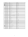
79 safety ref. No. Part no. Part name & description q'ty remarks 1 10030-0047500 battery cover 1 pavca 2 k2ahyh000034 ac inlet with cable 1 pavca 3 k2cg3yy00060 ac cord(usa) 1 pavca 4 md50h13c2a plasma display panel 1 pavca 5 n2qayb000485 remote controller 1 pavca 6 tbla3679 stand pole r 1 7 tbla368...
Page 80
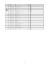
80 safety ref. No. Part no. Part name & description q'ty remarks 28 tsxl939 cable (c21-a34) 1 pavca 29 txfea01xser speaker l/r assy 2 pavca 30 txfkp02xser side terminal cover 1 pavca 31 txfku02xser rear cover 1 pavca 32 txfky01mduu cabinet assy 1 pavca txja11lquu speaker lead (a11-spr/spl) 1 pavca x...
Page 81
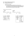
81 14.2. Electrical replacement parts list 14.2.1. Replacement parts list notes.
Page 82
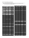
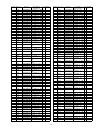
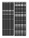
82 14.2.2. Electrical replacement parts list safety ref. No. Part no. Part name & description pcs remarks pcb txn/a1mduus circuit board a 1 (rtl)pa vca pcb n0ab5jk00001 circuit board p 1 pavca pcb txnc11lnuu circuit board c1 1 (rtl)pa vca pcb txnc21lnuu circuit board c2 1 (rtl)pa vca pcb txnsc1lnuu ...
Page 83
83 c4748 f1g1c104a116 c 0.10uf, k, 16v 1 c4749 f1g1h102a730 c 1000uf, 50v 1 c4750 f1g1c104a116 c 0.10uf, k, 16v 1 c4751 f1g1c104a116 c 0.10uf, k, 16v 1 c4752 f1g1c104a116 c 0.10uf, k, 16v 1 c4753 f1g1c104a116 c 0.10uf, k, 16v 1 c4754 f1g1c104a116 c 0.10uf, k, 16v 1 c4758 f1g1h102a730 c 1000uf, 50v 1...
Page 84
84 c8062 f1g1c104a116 c 0.10uf, k, 16v 1 c8063 f1g1h102a730 c 1000uf, 50v 1 c8064 f1g1a105a047 c 1uf, k, 10v 1 c8065 f1g1c104a116 c 0.10uf, k, 16v 1 c8067 f1g1a105a047 c 1uf, k, 10v 1 c8068 f1g1a105a047 c 1uf, k, 10v 1 c8069 f1g1c104a116 c 0.10uf, k, 16v 1 c8070 f1g1h102a730 c 1000uf, 50v 1 c8071 f1...
Page 85
85 c9335 f1j1a106a087 c 0.010uf, k, 10v 1 c9336 f1j1a106a087 c 0.010uf, k, 10v 1 c9337 f1j1a106a087 c 0.010uf, k, 10v 1 c9339 f1g1c104a116 c 0.10uf, k, 16v 1 c9340 f1g1c104a116 c 0.10uf, k, 16v 1 c9342 f1g1c104a116 c 0.10uf, k, 16v 1 c9344 f1g1c104a116 c 0.10uf, k, 16v 1 c9347 ecj1vb0j105k c 1uf, k,...
Page 86
86 c16724 f1k1e475a134 c 4.7uf, z, 25v 1 c16727 f1l2j1520001 c 1500uf, k,6.3v 1 c16753 f1k1e475a134 c 4.7uf, z, 25v 1 c16755 f1k1e475a134 c 4.7uf, z, 25v 1 c16756 f1k1e475a134 c 4.7uf, z, 25v 1 c16771 f1h1c105a145 c 0.01uf, k, 16v 1 c16773 f1k1e105a029 c 1uf, z, 25v 1 c16791 eeufc1e221 e 220uf, 25v ...
Page 87
87 d16721 b0echr000001 diode 1 d16722 da3df30acsrp zener diode 1 pavca d16724 da3df30acslw zener diode 1 pavca d16728 b0eckp000055 diode 1 d16765 b0eckp000055 diode 1 d16790 b0jcme000093 diode 1 d16820 b0accj000048 diode 1 d16821 dz2j330m0l zener diode 1 d16822 b0adcj000100 diode 1 d16824 dz2j330m0l...
Page 88
88 l16421 g0zz00002183 peaking coil 1 l16422 g0zz00002183 peaking coil 1 l16423 g0zz00002183 peaking coil 1 l16424 g0zz00002183 peaking coil 1 l16472 g0zz00002183 peaking coil 1 l16698 g0c681ma0065 peaking coil 1 l16851 g0zz00002183 peaking coil 1 pa4701 k5h5022a0031 fuse 1 pc16191 b3pba0000496 ic 1...
Page 89
89 r2311 erj2gej220 m 22 ohm, j,0.063w 1 r2314 d0ga303ja015 m 30k ohm j 0.063w 1 pavca r2315 d0ga303ja015 m 30k ohm j 0.063w 1 pavca r2316 d0ga303ja015 m 30k ohm j 0.063w 1 pavca r2324 d0ga471ja015 m 470ohm, j,0.063w 1 r2325 d0ga471ja015 m 470ohm, j,0.063w 1 r2326 d1bb2212a055 m22.1kohm, 1/10w 1 r23...
Page 90
90 r5630 d0ga101ja015 m 100 ohm, j,0.063w 1 r5631 d0ga471ja015 m 470ohm, j,0.063w 1 r5632 d0ga101ja015 m 100 ohm, j,0.063w 1 r5663 erj2gej104 m 100kohm, j,0.063w 1 r5667 d1bb4301a087 m4.3 kohm, 1/10w 1 pavca r5668 d1bb1002a087 m 10kohm, 1/10w 1 r5669 d1bb1202a087 m 12kohm, 1/10w 1 pavca r5670 d0ga22...
Page 91
91 r8317 d0ga473ja015 m 47 ohm, j,0.063w 1 r8318 d0ga223ja015 m 22k ohm j 0.063w 1 r8319 d0ga393ja015 m 39kohm,j,0.063w 1 r8321 d0ga472ja015 m 4.7kohm, j,0.063w 1 r8330 d0ga222ja015 m 2.2kohm, j,0.063w 1 r8331 d0ga472ja015 m 4.7kohm, j,0.063w 1 r8332 erj2gej220 m 22 ohm, j,0.063w 1 r8333 d0ga122ja01...
Page 92
92 r9324 d0gb162ja041 n 1.6kohm j 1/ 10w 1 r9325 d0gb162ja041 n 1.6kohm j 1/ 10w 1 r9326 d0gb162ja041 n 1.6kohm j 1/ 10w 1 r9327 d0gb162ja041 n 1.6kohm j 1/ 10w 1 r9400 exb2hv103jv resistor array 1 r9401 exb2hv103jv resistor array 1 r9608 exb38v470j resistor array 1 r9609 exb38v470j resistor array 1...
Page 93
93 r16476 erj3geyj472 m 4.7kohm,j,1/ 16w 1 r16478 d0gb562ja041 m 5.6kohm,j,1/ 10w 1 r16479 erj6geyj103v m 10k ohm j 1/ 10w 1 r16490 erj6rbd104 m 100kohm, 1/10w 1 r16491 erj6red114 m 110kohm, 1/10w 1 r16492 erj6red124 m 120kohm, 1/10w 1 r16493 erj6rbd6981v m69.8 ohm,f,1/ 10w 1 pavca r16494 d1bb2001a0...
Page 94
94 r16804 erj8geyj112 m 1.1kohm, j,1/ 8w 1 r16822 erj6enf8202 m 82kohm, 1/10w 1 r16823 erj6enf8202 m 82kohm, 1/10w 1 r16824 erj6enf3302 m 33kohm, 1/10w 1 r16825 erjt06j154v m 150kohm,f,0.25w 1 r16826 erj6geyj103v m 10k ohm j 1/ 10w 1 r16827 d0gb222ja041 m 2.2kohm,j,1/ 10w 1 r16829 d0gb102ja041 m 1ko...
Page 95
95 sc2 k1ky02b00012 2p connector 1 sc3 k1ka03a00596 3p connector 1 sc20 k1my30ba0345 30p connector 1 pavca sc41 k1ka09aa0707 9p connector 1 sc42 k1ka09aa0707 9p connector 1 sc46 k1ka09aa0707 9p connector 1 sc50 k1ka02aa0193 2p connector 1 sn2510 b3jb00000078 ic 1 pavca ss3 k1ky03ba0236 3p connector ...

