- DL manuals
- Z-World
- Motherboard
- BL1800
- User Manual
Z-World BL1800 User Manual
Summary of BL1800
Page 1
Jackrabbit (bl1800) c-programmable single-board computer user’s manual 019–00067 • 030131–e.
Page 2
Jackrabbit (bl1800) z-world, inc. 2900 spafford street davis, california 95616-6800 usa telephone: (530) 757-3737 fax: (530) 753-5141 www.Zworld.Com jackrabbit (bl1800) user’s manual part number 019-0067 • 030131–e • printed in u.S.A. ©2000–2003 z-world inc. • all rights reserved. Z-world reserves t...
Page 3: Able
User’s manual t able of c ontents chapter 1. Introduction 1 1.1 features .................................................................................................................................................1 1.2 development and evaluation tools...............................................
Page 4
Jackrabbit (bl1800) appendix c. Power management 45 c.1 power supplies .................................................................................................................................. 45 c.2 batteries and external battery connections....................................................
Page 5: 1. I
User’s manual 1 1. I ntroduction the jackrabbit is a high-performance, c-programmable control- ler with a compact form factor. A rabbit 2000™ microprocessor operating at 30 mhz provides fast data processing. 1.1 features • 30 mhz clock • 24 cmos-compatible i/o • 3 analog channels: 1 a/d input, 2 pwm...
Page 6
2 jackrabbit (bl1800) three versions of the jackrabbit are available. Their standard features are summarized in table 1. 1.2 development and evaluation tools a complete development kit, including a prototyping board and dynamic c develop- ment software, is available for the jackrabbit. The developme...
Page 7
User’s manual 3 1.3 how to use this manual this user’s manual is intended to give users detailed information on the jackrabbit. It does not contain detailed information on the dynamic c development environment or the rabbit 2000™ microprocessor. Most users will want more detailed information on some...
Page 8
4 jackrabbit (bl1800) 1.4 ce compliance equipment is generally divided into two classes. These limits apply over the range of 30–230 mhz. The limits are 7 db higher for frequen- cies above 230 mhz. Although the test range goes to 1 ghz, the emissions from rabbit- based systems at frequencies above 3...
Page 9
User’s manual 5 digital i/o cables. Your results may vary, depending on your application, so additional shielding or filtering may be needed to maintain the class b emission qualification. Note: if no ferrite absorbers are fitted, the jackrabbit boards will still meet en55022:1998 class a requiremen...
Page 10
6 jackrabbit (bl1800).
Page 11: 2. S
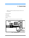
User’s manual 7 2. S ubsystems chapter 2 describes the principal subsystems and their use for the jackrabbit. • digital inputs/outputs • a/d converter • d/a converters • serial communication • memory figure 1 shows these rabbit-based subsystems designed into the jackrabbit. Figure 1. Jackrabbit subs...
Page 12
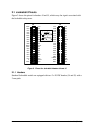
8 jackrabbit (bl1800) 2.1 jackrabbit pinouts figure 2 shows the pinout for headers j4 and j5, which carry the signals associated with the jackrabbit subsystems. Figure 2. Pinout for jackrabbit headers j4 and j5 2.1.1 headers standard jackrabbit models are equipped with two 2 × 20 idc headers (j4 and...
Page 13
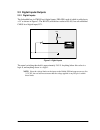
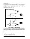
User’s manual 9 2.2 digital inputs/outputs 2.2.1 digital inputs the jackrabbit has six cmos-level digital inputs, pb0–pb5, each of which is pulled up to +5 v as shown in figure 3. The bl1820, which does not have rs-485, has one additional cmos-level digital input, pc1. Figure 3. Digital inputs the a...
Page 14
10 jackrabbit (bl1800) 2.2.2 digital outputs the jackrabbit has four cmos-level digital outputs, pb6–pb7, pclk, and ioben. Four high-power outputs, hv0–hv3, are also available—hv0–hv2 can each sink up to 1 a (200 ma for the bl1810 and bl1820) at 30 v, and hv3 can source up to 500 ma (100 ma for the ...
Page 15
User’s manual 11 2.2.2.1 configurable high-power output (hv3) hv3, shown schematically in figure 5, is factory-configured to be a sourcing output. Figure 5. Configurable high-current output when used as a sourcing output, hv3 is switched to k when pe3 on the rabbit 2000 goes high, and the two transi...
Page 16
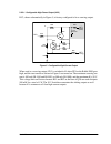
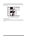
12 jackrabbit (bl1800) hv3 can also be reconfigured as a sinking output. To do so, remove the 0 Ω surface- mounted resistor r56, and solder on a 0 Ω surface-mounted resistor or jumper wire at r55. If you plan to drive inductive loads, add a diode at d21. Figure 6 shows the location of these componen...
Page 17
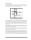
User’s manual 13 2.3 a/d converter the analog-to-digital (a/d) converter, shown in figure 7, compares the da0 voltage to ad0, the voltage presented to the converter. Da0 therefore cannot be used for the digital- to-analog (d/a) converter when the a/d converter is being used. Figure 7. Schematic diag...
Page 18
14 jackrabbit (bl1800) there is a 10 k Ω resistor, r31, connected between vcc and ad0. This resistor should pro- vide an appropriate voltage divider bias for a variety of common thermistors so that they can be connected directly between ad0 and ground. The a/d converter load is the 10 k Ω resistor c...
Page 19
User’s manual 15 2.4 d/a converters two digital-to-analog (d/a) converter outputs, da0 and da1, are supplied on the jack- rabbit. These are shown in figure 8. The d/a converters have no reference voltage. Although they may be fairly accurate from one programmed voltage to the next, they do not have ...
Page 20
16 jackrabbit (bl1800) it is very easy to do pulse-width modulation with the rabbit 2000 microprocessor because of the chip’s architecture. 2.4.1 da1 the op amp supporting da1 converts pulse-width modulated signals to an analog voltage between 0 v and 5 v. A digital signal that varies with time is f...
Page 21
User’s manual 17 either a 0% or a 100% duty cycle. The duty cycle is programmed as the high-time count of 1024 total counts of the rabbit 2000’s timer b. Thus, 256 counts would be 25% of 1024 counts, and corresponds to a 25% duty cycle. Table 2 lists typical da1 voltages measured for various duty cy...
Page 22
18 jackrabbit (bl1800) 2.4.2 da0 the op amp supporting da0 translates a 12%–88% duty cycle to an analog voltage range of 0 v to 3 v. The software operates only within this duty cycle; a duty cycle less than 12% is rounded down to 0%, and any duty cycle above 88% is rounded up to 100%. Da0 uses a vol...
Page 23
User’s manual 19 the resolution of the da0 output depends on the smallest increment of time to change the on/off time (the time between 5 v and 0 v). The jackrabbit uses the rabbit 2000’s port d control registers to clock out the signal at a timer timeout. The timer used is timer b. Timer b has 10 b...
Page 24
20 jackrabbit (bl1800) 2.5 serial communication the jackrabbit has two rs-232 (3-wire) serial channels, one rs-485 serial channel, and one synchronous cmos serial channel. 2.5.1 rs-232 the jackrabbit’s two rs-232 serial channels are connected to an rs-232 transceiver, u4, an industry-standard max232...
Page 25
User’s manual 21 figure 9. Multidrop jackrabbit network u4 vin gnd gnd reset jackrabbit z-world, inc. Gnd pa0 pa2 pa4 pa6 gnd pb0 pb2 pb4 pb6 wdo gnd pe6 pe4 pe2 pe0 hv0 hv2 k gnd vcc pa1 pa3 pa5 pa7 gnd pb1 pb3 pb5 pb7 pclk pe7 pe5 pe3 pe1 gnd hv1 hv3 +raw vcc gnd rxc txc pc1 pc3 pc5 pc7 agnd da1 p...
Page 26
22 jackrabbit (bl1800) the jackrabbit comes with a 220 Ω termination resistor and 681 Ω bias resistors already installed, as shown in figure 10. Figure 10. Rs-485 termination and bias resistors the load these bias and termination resistors present to the rs-485 transceiver (u6) limits the number of ...
Page 27
User’s manual 23 2.6 memory 2.6.1 sram the jackrabbit is designed to accept 32k to 512k of sram packaged in an soic case. Standard jackrabbit models come with 128k of sram. A factory-installed option for 512k of sram is available. Figure 11 shows the locations and the jumper settings for the jump- e...
Page 28
24 jackrabbit (bl1800) 2.7 other hardware 2.7.1 external interrupts jackrabbit boards that carry the ce mark have external interrupts available on digital inputs pe4 and pe5. 2.7.2 clock doubler jackrabbit bl1810 and bl1820 models take advantage of the rabbit 2000 microproces- sor’s internal clock d...
Page 29
User’s manual 25 2.7.3 spectrum spreader jackrabbit boards that carry the ce mark have a rabbit 2000 microprocessor that features a spectrum spreader, which helps to mitigate emi problems. By default, the spectrum spreader is on automatically for jackrabbit bl1810 and bl1820 boards that carry the ce...
Page 30
26 jackrabbit (bl1800).
Page 31: Ppendix
User’s manual 27 a ppendix a. S pecifications appendix a provides the specifications for the jackrabbit..
Page 32
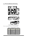
28 jackrabbit (bl1800) a.1 electrical and mechanical specifications figure a-1 shows the mechanical dimensions for the jackrabbit. Figure a-1. Jackrabbit (bl1810) dimensions table a-1 provides the pin 1 locations for the jackrabbit headers. Table a-1. Jackrabbit header pin 1 locations header descrip...
Page 33
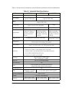
User’s manual 29 table a-2 lists the electrical, mechanical, and environmental specifications for the jackrabbit boards. Table a-2. Jackrabbit board specifications parameter bl1800 bl1810 bl1820 microprocessor rabbit 2000 @ 29.5 mhz rabbit 2000 @ 14.7 mhz flash eprom 256k (supports 128k–512k) 128k (...
Page 34
30 jackrabbit (bl1800) a.2 jumper configurations figure a-2 shows the header and jumper locations used to configure the various jackrabbit options. Figure a-2. Location of jackrabbit configurable positions r55 r56 d21 c27 d24 jp2 r16 r17 r18 jp1 z-world, inc. Jackrabbit jp3 top side bottom side caut...
Page 35
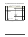
User’s manual 31 table a-3 lists the configuration options. 0 Ω surface mount resistors are used for all the header positions. Note: header jp3 is available only on jackrabbit boards labeled 175-0255. These boards were introduced in 2003. Table a-3. Jackrabbit jumper configurations header descriptio...
Page 36
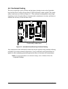
32 jackrabbit (bl1800) a.3 conformal coating the areas around the crystal oscillator and the battery backup circuit on the jackrabbit have had the dow corning silicone-based 1-2620 conformal coating applied. The confor- mally coated areas are shown in figure a-3. The conformal coating protects these...
Page 37
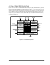
User’s manual 33 a.4 use of rabbit 2000 parallel ports figure a-4 shows the use of the rabbit 2000 parallel ports. The jackrabbit has 27 general- purpose digital inputs/outputs available on headers j4 and j5—15 are bidirectional (one of which is used by the rs-485 chip on bl1800 and bl1810 models), ...
Page 38
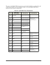
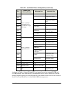
34 jackrabbit (bl1800) the ports on the rabbit 2000 microprocessor used in the jackrabbit are configurable, and so the factory defaults can be reconfigured. Table a-4 lists the rabbit 2000 factory defaults and the alternate configurations. Table a-4. Jackrabbit pinout configrations pin rabbit 2000 f...
Page 39
User’s manual 35 as shown in table a-4, pins pe4 and pe5 can instead be used as external int0b and int1b interrupts. Pins pd6 and pd7 can instead be used to access serial port a on the rabbit 2000 microprocessor. Pins pb0 and pb1 can instead be used to access the clock on serial port b and serial po...
Page 40
36 jackrabbit (bl1800) the four output-only pins are located on pb6–pb7, pclk, and ioben. Pb7 can also be used with the slave port of the rabbit 2000 microprocessor. The primary function of pclk is as a peripheral clock or a peripheral clock ÷ 2, but pclk can instead be used as a digital output. Sim...
Page 41: Ppendix
User’s manual 37 a ppendix b. P rototyping b oard appendix b describes the features and accessories of the proto- typing board, and explains the use of the prototyping board to demonstrate the jackrabbit and to build prototypes of your own circuits..
Page 42
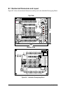
38 jackrabbit (bl1800) b.1 mechanical dimensions and layout figure b-1 shows the mechanical dimensions and layout for the jackrabbit prototyping board. Figure b-1. Jackrabbit prototyping board pc2 pc0 txb rxb vcc rxc txc pc1 pc3 gnd txc rxc j1 rxb txb gnd j7 gnd pa 6 pa 4 pa 2 pa 0 pa 5 pa 3 pa 1 pa...
Page 43
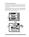
User’s manual 39 b.2 using the prototyping board the prototyping board is actually both a demonstration board and a prototyping board. As a demonstration board, it can be used to demonstrate the functionality of the jackrabbit right out of the box without any modifications to either board. There are...
Page 44
40 jackrabbit (bl1800) b.2.1 demonstration board a relay, a thermistor, four additional leds, and a serial cable are included in a bag of parts to further allow exploration of the jackrabbit‘s operation. The spdt relay handles 120 v at 5 a with a 12 v activating coil. The layout to accept this relay...
Page 45
User’s manual 41 the thermistor has a nominal room-temperature resistance of about 10 k Ω , which drops to about 6 k Ω at 40°c. Once you solder the thermistor onto the rt1 pads (see figure b-4) on the prototyping board, the a/d readings on ad0 will change with temperature. If the 10 k Ω potentiomete...
Page 46
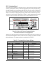
42 jackrabbit (bl1800) b.2.2 prototyping board to maximize the availability of jackrabbit resources, the demonstration hardware (leds, switches, potentiometer, buzzer) on the prototyping board may be disconnected. This is done by cutting the traces seen between and within the silk-screen outline of ...
Page 47
User’s manual 43 once the leds, resistors, and switches are disconnected as described above, the user has a jackrabbit board with connection points conveniently brought out to labeled points at headers j3 and j7 on the prototyping board. Small to medium circuits can be prototyped using point- to-poi...
Page 48
44 jackrabbit (bl1800).
Page 49: Ppendix
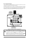
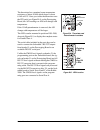
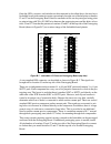
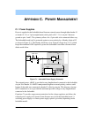
User’s manual 45 a ppendix c. P ower m anagement c.1 power supplies power is supplied to the jackrabbit board from an external source through either header j1 or header j4. J1 is a 3-pin straight header with a pitch of 0.1". V in is on pin 2 between ground on pins 1 and 3. The symmetry allows for a ...
Page 50
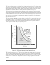
46 jackrabbit (bl1800) the linear voltage regulator is simply a fixed-voltage regulator with a ±5% voltage output tolerance as the temperature changes. The regulator has a small heat sink, which increases the maximum external input voltage. Higher external input voltages increase the voltage dropped...
Page 51
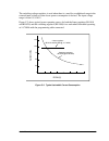
User’s manual 47 the switching voltage regulator is used when there is a need for an additional range in the external input voltage or when lower power consumption is desired. The input voltage range is from 8 v to 40 v. Figure c-3 shows typical power operating curves for both the linear regulator (...
Page 52
48 jackrabbit (bl1800) c.2 batteries and external battery connections the soldered-in 950 ma·h lithium coin cell provides power to the real-time clock and sram when external power is removed from the circuit. This allows the jackrabbit to continue to keep track of time and preserves the sram memory ...
Page 53
User’s manual 49 c.2.1 battery backup circuit figure c-5 shows the jackrabbit battery backup circuitry. Figure c-5. Jackrabbit battery backup circuit resistor r12, shown in figure c-5, is typically not stuffed on the jackrabbit board. Vram and vcc are equal when power is supplied to the jackrabbit. ...
Page 54
50 jackrabbit (bl1800) the battery-backup circuit serves two purposes: • it reduces the battery voltage to the real-time clock, thereby reducing the current con- sumed by the real-time clock and lengthening the battery life. • it ensures that current can flow only out of the battery to prevent charg...
Page 55
User’s manual 51 c.3 chip select circuit figure c-7 shows a schematic of the chip select circuit. Figure c-7. Chip select circuit the current drain on the battery in a battery-backed circuit must be kept at a minimum. When the jackrabbit board is not powered, the battery keeps the sram memory conten...
Page 56
52 jackrabbit (bl1800) transistors q20 and q21 are of opposite polarity so that a rail-to-rail voltages can be passed. When the /cs1 voltage is low, q20 will conduct. When the /cs1 voltage is high, q21 will conduct. It takes time for the transistors to turn on, creating a propagation delay. This del...
Page 57: Ppendix
User’s manual 53 a ppendix d. A lternate u se of the p rogramming p ort appendix d provides additional information for the program- ming port in association with the diag and prog connectors on the programming cable. The prog connector is used only when the programming cable is attached to the progr...
Page 58
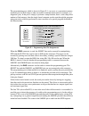
54 jackrabbit (bl1800) the programming port, which is shown in figure d-1, can serve as a convenient commu- nications port for field setup or other occasional communication need (for example, as a diagnostic port). If the port is simply to perform a setup function, that is, write setup infor- mation...
Page 59: Otice
User’s manual 55 n otice to u sers zworld products are not authorized for use as critical components in life- support devices or systems unless a specific written agreement regarding such intended use is entered into between the customer and z-world prior to use. Life-support devices or systems are ...
Page 60
56 jackrabbit (bl1800).
Page 61: Ndex
User’s manual 57 i ndex a a/d converter ................. 13, 14 additional information getting started manual ....... 3 online documentation .......... 3 b backup battery ................. 48, 49 chip select circuit .............. 50 external battery connec- tions ............................. 48 c...
Page 62
58 jackrabbit (bl1800).
Page 63: Chematics
User’s manual 59 s chematics 090-0092 jackrabbit schematic www.Zworld.Com/documentation/schemat/090-0092.Pdf 090-0088 jackrabbit prototyping board schematic www.Zworld.Com/documentation/schemat/090-0088.Pdf 090-0128 programming cable schematic www.Zworld.Com/documentation/schemat/090-0128.Pdf the sc...
Page 64
60 jackrabbit (bl1800).

