- DL manuals
- 4DSP
- Control Unit
- AD484
- User Manual
4DSP AD484 User Manual
AD484 user manual
V1.2
AD484
User Manual
4DSP Inc.
955 S Virginia Street, Suite 214, Reno, NV 89502, USA
Email:
support@4dsp.com
This document is the property of 4DSP Inc. and may not be copied nor communicated to a
third party without the written permission of 4DSP Inc.
©
4DSP Inc. 2007
id4651869 pdfMachine by Broadgun Software - a great PDF writer! - a great PDF creator! - http://www.pdfmachine.com http://www.broadgun.com
Summary of AD484
Page 1
Ad484 user manual v1.2 ad484 user manual 4dsp inc. 955 s virginia street, suite 214, reno, nv 89502, usa email: support@4dsp.Com this document is the property of 4dsp inc. And may not be copied nor communicated to a third party without the written permission of 4dsp inc. © 4dsp inc. 2007 id4651869 p...
Page 2: Ad484 User Manual
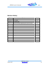
Ad484 user manual v1.2 ad484 user manual february 2007 www.4dsp.Com - 2 - revision history date revision version 02-03-07 first release 1.0 03-29-07 corrected typos 1.1 04-12-07 added more details regarding clock synchronization 1.2.
Page 3: Ad484 User Manual
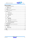
Ad484 user manual v1.2 ad484 user manual february 2007 www.4dsp.Com - 3 - table of contents 1 acronyms and related documents ............................................................................. 4 1.1 acronyms......................................................................................
Page 4: Ad484 User Manual
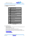
Ad484 user manual v1.2 ad484 user manual february 2007 www.4dsp.Com - 4 - 1 acronyms and related documents 1.1 acronyms adc analog to digital converter dac digital to analog converter dci digitally controlled impedance ddr double data rate dsp digital signal processing eprom erasable programmable re...
Page 5: Ad484 User Manual
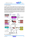
Ad484 user manual v1.2 ad484 user manual february 2007 www.4dsp.Com - 5 - 1.3 general description the ad484 is a high performance pmc/xmc digitizer module dedicated to digital signal processing applications with high bandwidth and complex algorithms requirements. The ad484 can interface to a pci-exp...
Page 6: Ad484 User Manual
Ad484 user manual v1.2 ad484 user manual february 2007 www.4dsp.Com - 6 - the ad484 converts 4 analogue signals into four 14-bit resolution digital data flows with a sampling frequency up to 125mhz. The clock source can be set to external or internal using the software and firmware settings availabl...
Page 7: Ad484 User Manual
Ad484 user manual v1.2 ad484 user manual february 2007 www.4dsp.Com - 7 - 3.1.1.4 pci interface the virtex-4 device a interfaces directly to the pci bus via the pmc pn1, pn2 and pn3 connectors or to the pci-e bus via the pn5. An embedded pci core from xilinx is used to communicate over the pci bus w...
Page 8: Ad484 User Manual
Ad484 user manual v1.2 ad484 user manual february 2007 www.4dsp.Com - 8 - 3.1.1.6 pn4 user i/o connector the pn4 connector is wired to the virtex-4 device a. The 32 lower bits are available only if an xc4vfx60 device is mounted on board. The 32 higher bits are available only if pci 32-bit is used an...
Page 9: Ad484 User Manual
Ad484 user manual v1.2 ad484 user manual february 2007 www.4dsp.Com - 9 - 3.1.2 virtex-4 device b 3.1.2.1 virtex-4 device b family and package the virtex-4 device b is dedicated to interfacing to the a/d circuitry and can also perform digital signal processing algorithms. It is available in the virt...
Page 10: Ad484 User Manual
Ad484 user manual v1.2 ad484 user manual february 2007 www.4dsp.Com - 10 - 3.2 fpga devices configuration 3.2.1 flash storage the fpga firmware is stored on board in a flash device. The 128mbit device is partly used to store the configuration for both fpgas. In the default cpld firmware configuratio...
Page 11: Ad484 User Manual
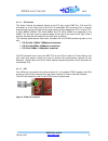
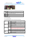
Ad484 user manual v1.2 ad484 user manual february 2007 www.4dsp.Com - 11 - figure 4: switch (j1) location off default setting. The virtex-4 device a configuration is loaded from the flash at power up. Sw1 on virtex-4 device a safety configuration loaded from the flash at power up. To be used only if...
Page 12: Ad484 User Manual
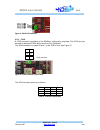
Ad484 user manual v1.2 ad484 user manual february 2007 www.4dsp.Com - 12 - figure 5: cpld led locations 3.2.3 jtag a jtag connector is available on the ad484 for configuration purposes. The jtag can also be used to debug the fpga design with the xilinx chipscope. The jtag connector is located on sid...
Page 13: Ad484 User Manual
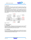
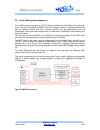
Ad484 user manual v1.2 ad484 user manual february 2007 www.4dsp.Com - 13 - 3.3 clock tree the ad484 clock architecture offers an efficient distribution of low jitter clocks. In addition to the pci express bus, the mgt reference clocks of 106.25mhz and 125mhz (epson eg2121ca) make it possible to impl...
Page 14: Ad484 User Manual
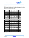
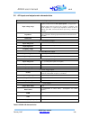
Ad484 user manual v1.2 ad484 user manual february 2007 www.4dsp.Com - 14 - 3.5 a/d inputs and outputs main characteristics analogue inputs input voltage range ac coupled option. 2.4 vp-p (11.5 dbm –50 ohm) full scale - ac coupled via rf transformer. Dc coupled option. 1.15 vp-p (gain amplifier 6db) ...
Page 15: Ad484 User Manual
Ad484 user manual v1.2 ad484 user manual february 2007 www.4dsp.Com - 15 - 3.5.1 analog inputs the module is built around four ti ads5500 14-bit sampling analog-to-digital. Adcs: analog data enters the module via four sma connectors on the front panel, one for each channel. Both signals are then con...
Page 16: Ad484 User Manual
Ad484 user manual v1.2 ad484 user manual february 2007 www.4dsp.Com - 16 - 3.6 front panel optical transceivers four 2.5gb/s optical transceivers (ltp-st11m) are available on the ad484 in the front panel area. They are connected to the mgt i/os of the virtex-4 device a. Infiniband protocols as well ...
Page 17: Ad484 User Manual
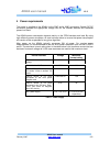
Ad484 user manual v1.2 ad484 user manual february 2007 www.4dsp.Com - 17 - 4 power requirements the power is supplied to the ad484 via the pmc and/or xmc connectors. Several dc-dc converters generate the appropriate voltage rails for the different devices and interfaces present on board. The ad484 p...
Page 18: Ad484 User Manual
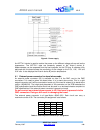
Ad484 user manual v1.2 ad484 user manual february 2007 www.4dsp.Com - 18 - figure 9 : power supply an adt7411 device is used to monitor the power on the different voltage rails as well as the temperature. The adt7411 data are constantly passed to the virtex-4 device a. Measurements can be accessed f...
Page 19: Ad484 User Manual
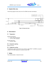
Ad484 user manual v1.2 ad484 user manual february 2007 www.4dsp.Com - 19 - 5 system side view the following diagram shows a side view of the ad484 mounted a motherboard. Figure 10: system side view 6 environment 6.1 temperature operating temperature 0 ° c to +60 ° c (commercial) -40 ° c to +85 ° c (...
Page 20: Ad484 User Manual
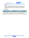
Ad484 user manual v1.2 ad484 user manual february 2007 www.4dsp.Com - 20 - 8 emc this module is designed to operate from within an enclosed host system, which is build to provide emc shielding. Operation within the eu emc guidelines is not guaranteed unless it is installed within an adequate host sy...

