- DL manuals
- 4DSP
- PCI Card
- FC6301
- User Manual
4DSP FC6301 User Manual
Summary of FC6301
Page 1
Um027 fc6301 user manual r1.3 um027 www.4dsp.Com - 1 - fc6301 user manual 4dsp llc, usa email: support@4dsp.Com this document is the property of 4dsp llc and may not be copied nor communicated to a third party without the written permission of 4dsp llc © 4dsp llc 2013.
Page 2: Revision History
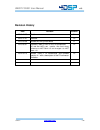
Um027 fc6301 user manual r1.3 um027 www.4dsp.Com - 2 - revision history date revision revision 2010-10-05 draft 0.1 2010-11-21 release 1.0 2013-04-08 added the fmc pinout tables 1.1 2013-05-01 updated table 5: fmc gtx/gth connections to use the mgtx_abc notation. Also fixed wrong reference to mgt ba...
Page 3: Table Of Contents
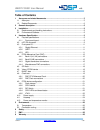
Um027 fc6301 user manual r1.3 um027 www.4dsp.Com - 3 - table of contents 1 acronyms and related documents ............................................................................. 5 1.1 acronyms ........................................................................................................
Page 4
Um027 fc6301 user manual r1.3 um027 www.4dsp.Com - 4 - appendix a: errata .............................................................................................................27.
Page 5
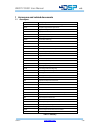
Um027 fc6301 user manual r1.3 um027 www.4dsp.Com - 5 - 1 acronyms and related documents 1.1 acronyms a/d analog to digital converter blast board level advanced scalable technology cpld complex programmable logic device d/a digital to analog converter dci digitally controlled impedance ddr double dat...
Page 6
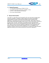
Um027 fc6301 user manual r1.3 um027 www.4dsp.Com - 6 - 1.2 related documents 3u compactpci specifications (picmg 2.0 r3.0) compactpci hot swap specifications (picmg 2.1 r2.0) vita 57.1 fpga mezzanine card standard xilinx virtex-6 documentation 2 general description the fc6301 is a high performance c...
Page 7
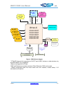
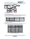
Um027 fc6301 user manual r1.3 um027 www.4dsp.Com - 7 - blast 1 blast blast xc6vlx240t xc6vlx365t xc6vlx550t xc6vsx315t xc6vsx475t jtag cpld led x4 optional fmc 3 vita 57 1 0 x m g t 3 .1 2 5 g b p s cpci j1 32-bit 33/66mhz cpld pcie x1 pcie x1 to pci bridge cpci j2 user i/o virtex-6 blast 512mbit pa...
Page 8
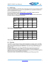
Um027 fc6301 user manual r1.3 um027 www.4dsp.Com - 8 - 3 installation 3.1 requirements and handling instructions the fc6301 daughter card must be installed cpci backplane compliant to the cpci standard. Do not flex the board and prevent electrostatic discharges by observing esd precautions when hand...
Page 9
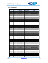
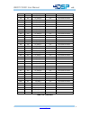
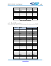
Um027 fc6301 user manual r1.3 um027 www.4dsp.Com - 9 - 4.1.2 p2 connections fpga pin p2 pin # signal name bank voltage notes at26 a1 fp_rtm_0 1.8v not available on lx240t au27 a2 fp_rtm_1 1.8v not available on lx240t ak23 b6 fp_rtm_10 1.8v not available on lx240t bb26 b8 fp_rtm_11 1.8v not available...
Page 10
Um027 fc6301 user manual r1.3 um027 www.4dsp.Com - 10 - h26 a20 fp_rtm_44 1.8v not available on lx240t g26 a21 fp_rtm_45 1.8v not available on lx240t f26 b12 fp_rtm_46 1.8v not available on lx240t k25 b14 fp_rtm_47 1.8v not available on lx240t j25 b16 fp_rtm_48 1.8v not available on lx240t b27 b18 f...
Page 11
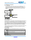
Um027 fc6301 user manual r1.3 um027 www.4dsp.Com - 11 - 4.2 cpci p0 connector a one lane pci express is connected to a bridge device (pi7c9x110) thus making the virtex- 6 fpga available for access on the parallel pci bus. The following performances have been recorded on the bus. pci 33 mhz: host t...
Page 12
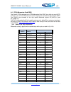
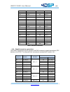
Um027 fc6301 user manual r1.3 um027 www.4dsp.Com - 12 - 4.4 fpga mezzanine card (fmc) the virtex-6 fpga interfaces to an fpga mezzanine card (fmc) via a high pin count (hpc) vita 57.1 site. All the differential and control signals are connected to the virtex-6 fpga. The fc6301 also connects all ten ...
Page 13
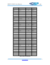
Um027 fc6301 user manual r1.3 um027 www.4dsp.Com - 13 - y37 la_n14 c19 la14_n w37 la_p14 c18 la14_p y35 la_n15 h20 la15_n aa35 la_p15 h19 la15_p aa30 la_n16 g19 la16_n y30 la_p16 g18 la16_p ab31 la_n17_cc d21 la17_n_cc aa31 la_p17_cc d20 la17_p_cc v30 la_n18_cc c23 la18_n_cc w30 la_p18_cc c22 la18_p...
Page 14
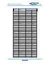
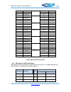
Um027 fc6301 user manual r1.3 um027 www.4dsp.Com - 14 - fpga pin net name fmc hpc pin number pin name ae32 ha_n00_cc f5 ha00_n_cc ad32 ha_p00_cc f4 ha00_p_cc aj35 ha_n01_cc e3 ha01_n_cc ah34 ha_p01_cc e2 ha01_p_cc am42 ha_n02 k8 ha02_n al42 ha_p02 k7 ha02_p am41 ha_n03 j7 ha03_n al41 ha_p03 j6 ha03_...
Page 15
Um027 fc6301 user manual r1.3 um027 www.4dsp.Com - 15 - ab36 ha_n19 f20 ha19_n ac36 ha_p19 f19 ha19_p ab33 ha_n20 e19 ha20_n ab32 ha_p20 e18 ha20_p ab42 ha_n21 k20 ha21_n aa42 ha_p21 k19 ha21_p ab41 ha_n22 j22 ha22_n aa41 ha_p22 j21 ha22_p aa40 ha_n23 k23 ha23_n ab39 ha_p23 k22 ha23_p table 4: fmc h...
Page 16
Um027 fc6301 user manual r1.3 um027 www.4dsp.Com - 16 - r42 hb_n12 f32 hb12_n p42 hb_p12 f31 hb12_p t36 hb_n13 e31 hb13_n u36 hb_p13 e30 hb13_p t40 hb_n14 k35 hb14_n r40 hb_p14 k34 hb14_p t35 hb_n15 j34 hb15_n t34 hb_p15 j33 hb15_p t42 hb_n16 f35 hb16_n t41 hb_p16 f34 hb16_p j38 hb_n17_cc k38 hb17_n...
Page 17
Um027 fc6301 user manual r1.3 um027 www.4dsp.Com - 17 - aj1 dp_c2m_p3 a30 dp3_c2m_p af4 dp_m2c_n3 a11 dp3_m2c_n af3 dp_m2c_p3 a10 dp3_m2c_p ag2 dp_c2m_n4 mgt3_113 a35 dp4_c2m_n ag1 dp_c2m_p4 a34 dp4_c2m_p ad4 dp_m2c_n4 a15 dp4_m2c_n ad3 dp_m2c_p4 a14 dp4_m2c_p ac2 dp_c2m_n5 mgt1_114 a39 dp5_c2m_n ac...
Page 18
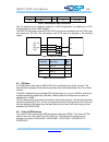
Um027 fc6301 user manual r1.3 um027 www.4dsp.Com - 18 - ah40 prsnt_m2c_l i h2 prsnt_m2c_l aj42 pg_c2m o d1 pg_c2m table 7: miscellaneous fmc connections the i/o standard to be assigned depends on vadj configuration, by default this is 2v5. Contact factory for other vadj voltages. The fmc i2c bus sig...
Page 19
Um027 fc6301 user manual r1.3 um027 www.4dsp.Com - 19 - 4.7 blast sites thanks to the availability of 3 blast sites a wide variety of memory and processing modules can be connected to the virtex-6 device. For each blast site it is possible to choose from the list of available blast modules. For more...
Page 20
Um027 fc6301 user manual r1.3 um027 www.4dsp.Com - 20 - virtex-6 fpga 50mhz crystal cpld vita 57.1 fmc cdcv304 clock synthesizer cdcel925 pcie-pci bridge 100mhz low jitter lvds jitter attenuator and buffer mgt fmc ref clk mgt 16 mhz crystal cpci clock 33/66 mhz figure 5 : clock tree 4.8.1 fmc gtx re...
Page 21
Um027 fc6301 user manual r1.3 um027 www.4dsp.Com - 21 - 4.9 fpga device configuration 4.9.1 flash storage the fpga firmware is stored on board in a flash device. The 512mbit device is partly used to store the configuration for both fpgas. In the default cpld firmware configuration, the virtex-6 devi...
Page 22
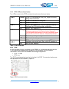
Um027 fc6301 user manual r1.3 um027 www.4dsp.Com - 22 - 4.9.4 cpld leds and board status four leds connect to the cpld and give information about the board status. Led 0 flashing virtex-6 fpga bitstream or user_rom_register is currently being written to the flash on virtex-6 fpga device not configur...
Page 23
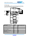
Um027 fc6301 user manual r1.3 um027 www.4dsp.Com - 23 - 4.10 power supply the power is supplied to the fc6301 via the compactpci connectors. Several dc-dc converters generate the appropriate voltage rails for the different devices and interfaces present on board. The fc6301 power distribution is as ...
Page 24
Um027 fc6301 user manual r1.3 um027 www.4dsp.Com - 24 - table 15 : power supply 4.11 hotswap hot swap is the act of removal and insertion of cards into a platform while that system is operational. This process should not cause any failures on the systems power supply and system’s i/o signals. Protec...
Page 25
Um027 fc6301 user manual r1.3 um027 www.4dsp.Com - 25 - parameter: device 2 formula on-chip temperature adt7411 die temperature on-chip ain0 (v dd ) +3.3v external ain1 blast0_vcore ain1 external ain2 blast2_vcore ain2 external ain3 5v ain3*(1249/249) external ain4 0v9 ain4 external ain5 vadj ain5 e...
Page 26
Um027 fc6301 user manual r1.3 um027 www.4dsp.Com - 26 - 5 environment 5.1 temperature operating temperature 0 ° c to +60 ° c (commercial) -40 ° c to +85 ° c (industrial) storage temperature: -40 ° c to +120 ° c 5.2 convection cooling the air flow provided by the chassis fans the fc6301 is enclosed i...
Page 27
Um027 fc6301 user manual r1.3 um027 www.4dsp.Com - 27 - appendix a: errata pcb revision 2.1 spi flash not supported..


