- DL manuals
- Aaeon
- Computer Hardware
- ECB-901A
- Quick Installation Manual
Aaeon ECB-901A Quick Installation Manual
Summary of ECB-901A
Page 1
C a r r i e r b o a r d e c b - 9 0 1 a quick installation guide - 1 - quick installation guide part no. 2007901a12 printed in taiwan june. 2005.
Page 2
C a r r i e r b o a r d e c b - 9 0 1 a quick installation guide - 2 - safety precautions always completely disconnect the power cord from your board whenever you are working on it. Do not make connections while the power is on, because a sudden rush of power can damage sensitive electronic componen...
Page 3
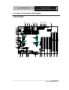
C a r r i e r b o a r d e c b - 9 0 1 a quick installation guide - 3 - 1. Location of connectors and jumpers component side cn12 cn26 cn14 cn18 jp14 pci1 pci2 pci3 pci4 cn3 cn2 cn1 cn9 cn24 jp12 jp13 jp11 cn13 etx3 jp10 jp9 cn23 jp4 cn11 jp15 jp18 jp17 jp16 cn22 jp8 jp23 jp7 jp3 jp6 cn20 cn21 ide1 i...
Page 4
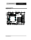
C a r r i e r b o a r d e c b - 9 0 1 a quick installation guide - 4 - 2. Mechanical drawing 0 0 13.29 36.81 53.31 93.45 99.14 122.25 134.75 147.25 7.41 19.53 9.99 8.07 3.23 10.17 163.88 168.36 40.02 41.29 38.11 59.84 88.28 92.72 96.53 120.66 146.49 148.5 150.51 169.56 173.37 177.81 172.1 182.26 204...
Page 5
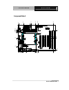
C a r r i e r b o a r d e c b - 9 0 1 a quick installation guide - 5 - 288.37 10.17 288.37 165.11 67.39 144.23 163.21 109.3 151.85 87.64 154.95 146.49 97.17 88.91 42.56 38.11 163.88 165.11 163.88 145.18 146.08 55.92 101.72 94.32 135.92 50.92 140.92 46.44 14.05 99.71 171.46 160.03 148.5 150.51 6.4 16...
Page 6: Jumpers
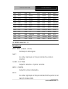
C a r r i e r b o a r d e c b - 9 0 1 a quick installation guide - 6 - 3. List of jumpers the board has a number of jumpers that allow you to configure your system to suit your application. The table below shows the function of each of the board's jumpers: jumpers label function jp1 doc address sele...
Page 7: Connectors
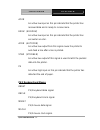
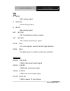
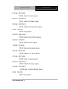
C a r r i e r b o a r d e c b - 9 0 1 a quick installation guide - 7 - jp24 5vsb for etx module 4. List of connectors the board has a number of connectors that allow you to configure your system to suit your application. The table below shows the function of each board's connectors: connectors label...
Page 8
C a r r i e r b o a r d e c b - 9 0 1 a quick installation guide - 8 - cn18 audio line-out connector cn19 audio microphone-in connector cn20 atx power connector cn21 at power connector cn22 fan connector cn23 backlight power connector cn24(com2) rs-232 serial port connector cn26 usb+rj45 connector c...
Page 9
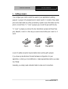
C a r r i e r b o a r d e c b - 9 0 1 a quick installation guide - 9 - 5. Setting jumpers you configure your card to match the needs of your application by setting jumpers. A jumper is the simplest kind of electric switch. It consists of two metal pins and a small metal clip (often protected by a pl...
Page 10
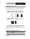
C a r r i e r b o a r d e c b - 9 0 1 a quick installation guide - 10 - 6. Doc address selection (jp1) the diskonchip 2000 occupies an 8 k byte window in the upper memory address range of cc00 to dc00. You should ensure this does not conflict with any other device's memory address. These addresses m...
Page 11
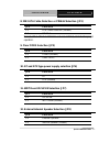
C a r r i e r b o a r d e c b - 9 0 1 a quick installation guide - 11 - 8. Ide2 ata cable detection or pdiag# selection (jp3) jp3 function 1-2 ata cable detection (default) 2-3 pdiag# remark: when ide2 and cn7 have devices installed, select 2-3 for proper operation. 9. Clear cmos selection (jp5) jp5...
Page 12
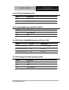
C a r r i e r b o a r d e c b - 9 0 1 a quick installation guide - 12 - 13. Lcd power selection (jp9) jp9 function 1-2 5v 2-3 3.3v (default) 14. Lcd backlight power selection (jp10) jp10 function 1-2 12v (default) 2-3 +5v 15. Com 2 rs-232/422/485 selection (jp11 & jp12) jp11 jp12 function 1-2, 4-5, ...
Page 13
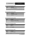
C a r r i e r b o a r d e c b - 9 0 1 a quick installation guide - 13 - 17. Etx-4 pin d90 selection (jp16) jp16 function 1-2 lan wakeup (lwake) 2-3 primary ide ata33/100 detect (pd_80p) (default) 18. Etx-4 pin d19 selection (jp17) jp17 function 1-2 ovcr# (usb) (default) 2-3 dack2# 19. Etx-4 pin d35 ...
Page 14
C a r r i e r b o a r d e c b - 9 0 1 a quick installation guide - 14 - 22. Etx-4 pin d26 selection (jp21) jp21 function 1-2 on cpu fan 1-2 off n.C. (default) 23. Etx-4 pin d41 selection (jp22) jp22 function 1-2 on secondary ide ata33/100 detect 1-2 off n.C. (default) 24. Front panel connector (jp4)...
Page 15
C a r r i e r b o a r d e c b - 9 0 1 a quick installation guide - 15 - 26. Fan power selection (jp23) jp23 function 1-2 5v 2-3 12v off 5v 27. 5vsb for etx module (jp24) jp24 function on standby 5v(5vsb) for etx module off no standby 5v(5vsb) for etx module 28. Rs-232 serial port connector (cn5, cn6...
Page 16
C a r r i e r b o a r d e c b - 9 0 1 a quick installation guide - 16 - 5 sdd6 30 sdd14 6 sdd7 31 sdd15 7 sdcs#1 32 sdcs#3 8 gnd 33 gnd 9 gnd 34 sdior# 10 gnd 35 sdiow# 11 gnd 36 +5v 12 gnd 37 irq15 13 +5v 38 +5v 14 gnd 39 csel# 15 gnd 40 n.C. 16 gnd 41 sec_iderst# 17 gnd 42 siordy 18 sda2 43 n.C. 1...
Page 17
C a r r i e r b o a r d e c b - 9 0 1 a quick installation guide - 17 - 7 gnd 8 #index 9 gnd 10 #motora 11 gnd 12 #drive select b 13 gnd 14 #drive select a 15 gnd 16 #motor b 17 gnd 18 #dir 19 gnd 20 #step 21 gnd 22 #write data 23 gnd 24 #write gate 25 gnd 26 #track0 27 gnd 28 #write protect 29 gnd ...
Page 18
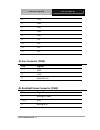
C a r r i e r b o a r d e c b - 9 0 1 a quick installation guide - 18 - 32. Digital io connector (cn10) pin signal pin signal 1 out0 2 out1 3 out2 4 out3 5 out4 6 out5 7 out6 8 out7 9 gnd 10 gnd 11 in0 12 in1 13 in2 14 in3 15 in4 16 in5 17 in6 18 in7 19 +5v 20 +12v 33. Tv out connector (cn11) pin si...
Page 19
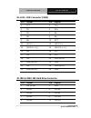
C a r r i e r b o a r d e c b - 9 0 1 a quick installation guide - 19 - 4 +5vsb 10 +5vsb 5 kb_clk 11 ms_clk 6 ms_clk 12 n.C. 35. Aaeon lvds connector (cn13) pin signal pin signal 1 backlight enable 2 backlight control 3 ppvcc 4 gnd 5 #lclk 6 lclk 7 ppvcc 8 gnd 9 #ldata0 10 ldata0 11 #ldata1 12 ldata...
Page 20
C a r r i e r b o a r d e c b - 9 0 1 a quick installation guide - 20 - 36. Vga display + printer + com connector (cn14) pin signal pin signal a1 #strobe a14 #afd a2 printer data0 a15 #error a3 printer data1 a16 #init a4 printer data2 a17 #slin a5 printer data3 a18 gnd a6 printer data4 a19 gnd a7 pr...
Page 21
C a r r i e r b o a r d e c b - 9 0 1 a quick installation guide - 21 - c9 +5v c10 gnd c11 nc c12 ddcdata c13 hsync c14 vsync c15 ddcclk 37. Atx power connector (cn20) pin signal pin signal 1 +3.3v 2 +3.3v 2 +3.3v 4 -12v 3 gnd 6 gnd 4 +5v 8 ps-on 5 gnd 10 gnd 6 +5v 12 gnd 7 gnd 14 gnd 8 pw-ok 16 -5v...
Page 22
C a r r i e r b o a r d e c b - 9 0 1 a quick installation guide - 22 - 4 -12v 5 gnd 6 gnd 7 gnd 8 gnd 9 -5v 10 +5v 11 +5v 12 +5v 39. Fan connector (cn22) pin signal 1 gnd 2 +12v 3 speed sense 40. Backlight power connector (cn23) pin signal 1 backlight power 2 & 3 gnd 4 backlight on.
Page 23
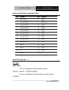
C a r r i e r b o a r d e c b - 9 0 1 a quick installation guide - 23 - 41. Lan + usb connector (cn26) pin signal pin signal 1 tct 2 td+ 3 td- 4 rd+ 5 rd- 6 na 7 na 8 na 9 na 10 rct 11 led1 (y-) 12 led1 (y+) 13 led2 (g-, o+) 14 led2 (g +, o-) 15 n.C. 16 n.C. 17 n.C. 18 n.C. 19 +5v 20 usb data0- 21 u...
Page 24
C a r r i e r b o a r d e c b - 9 0 1 a quick installation guide - 24 - 11 data3 12 data12 13 data2 14 data13 15 data1 16 data14 17 data0 18 data15 19 gnd 20 nc 21 req 22 gnd 23 io write 24 gnd 25 io read 26 gnd 27 io ready 28 gnd 29 dack 30 gnd 31 irq 32 nc 33 addr1 34 udma detect 35 addr0 36 addr2...
Page 25
C a r r i e r b o a r d e c b - 9 0 1 a quick installation guide - 25 - 44. Second printer connector (cn4) pin signal pin signal 1 #strobe 2 #afd 3 printer data0 4 #error 5 printer data1 6 #init 7 printer data2 8 #slin 9 printer data3 10 gnd 11 printer data4 12 gnd 13 printer data5 14 gnd 15 printer...
Page 26
C a r r i e r b o a r d e c b - 9 0 1 a quick installation guide - 26 - when this signals is asserted, a pci cycle is started. Devsel# device select signal. When the target device has decoded the address as its own cycle, it will assert devsel# trdy# target ready signal. When a device is ready to co...
Page 27
C a r r i e r b o a r d e c b - 9 0 1 a quick installation guide - 27 - please refer to below table for detailed. Pci slot 1 2 3 4 idsel ad19 ad20 ad21 ad31 int (pina6,b6,a7,b7) a, b, c, d b, c, d, a c, d, a, b d, a, b, c req/gnt req0# gnt0# req1# gnt1# req2# gnt2# req3# gnt3# pci clock pciclk0 pcic...
Page 28
C a r r i e r b o a r d e c b - 9 0 1 a quick installation guide - 28 - pme# pci device assert this signal for power management event. Usb usb0, usb0# (usbp0, usbp#0) usb port 0 signals. Usb0 is positive signal, usb0# is negative signal. They are differential pair. For proper operation, rout the two...
Page 29
C a r r i e r b o a r d e c b - 9 0 1 a quick installation guide - 29 - audio vccaud audio power 5v output. This power signal is fed by etx cpu module. Gndaud audio ground. Loutr right line-out signal. Loutl left line-out signal. Mic (mic-in) microphone input signal. Linr right line-in signal. Linl ...
Page 30
C a r r i e r b o a r d e c b - 9 0 1 a quick installation guide - 30 - serirq is not implemented. Serirq is default on etx module. Jp19 1-2 is off to set it as no connection as default on carrier board. Vcc 5v power input. This power signal is fed by etx carrier board. Resvd reserved. N.C no connec...
Page 31
C a r r i e r b o a r d e c b - 9 0 1 a quick installation guide - 31 - a31 c/be0# a32 ad7 a81 ad24 a82 cbe3# a33 ad8 a34 ad9 a83 vcc a84 vcc a35 gnd a36 gnd a85 ad25 a86 ad26 a37 ad10 a38 linl a87 ad28 a88 usb0 a39 ad11 a40 mic a89 ad27 a90 ad29 a41 ad12 a42 linr a91 ad30 a92 usb1 a43 ad13 a44 vcca...
Page 32
C a r r i e r b o a r d e c b - 9 0 1 a quick installation guide - 32 - iochck# i/o channel check signal. When i/o device parity error occurs, this signal is asserted. Iow# to write data to i/o port, this signal is asserted. Ior# to read data from i/o port, this signal is asserted. Smemw# to write d...
Page 33
C a r r i e r b o a r d e c b - 9 0 1 a quick installation guide - 33 - the isa bus cycle. Rstdrv (res-drv) this signal is asserted during power-on period and reset period. It is used to reset isa device. Refsh# (refresh#) this signal is used for i/o device to recharge on-board dram. Sysclk isa bus ...
Page 34
C a r r i e r b o a r d e c b - 9 0 1 a quick installation guide - 34 - this signal is asserted to indicated the end of a dma transfer, sbhe# this signal indicates that the high byte on the isa data bus is valid. M16# (memcs16#) memcs16# signal. This signal indicates that the bus size of current isa...
Page 35
C a r r i e r b o a r d e c b - 9 0 1 a quick installation guide - 35 - b27 la20 b28 n.C b77 sa18 b78 sa17 b29 la21 b30 irq11 b79 sa19 b80 smemr# b31 la22 b32 irq10 b81 iochrdy b82 aen b33 la23 b34 io16# b83 vcc b84 vcc b35 gnd b36 gnd b85 sd0 b86 smemw# b37 sbhe# b38 m16# b87 sd2 b88 sd1 b39 sa0 b4...
Page 36
C a r r i e r b o a r d e c b - 9 0 1 a quick installation guide - 36 - ack# an active low input on this pin indicate that the printer has received data and is ready to receive more. Err# (error#) an active low input on this pin indicate that the printer has encounter an error. Afd# (autofd#) an act...
Page 37
C a r r i e r b o a r d e c b - 9 0 1 a quick installation guide - 37 - vga r (red) red analog output. G (green) green analog output. B (blue) blue analog output. Hsy (hsync) crt horizontal synchronous signal. Vsy (vsync) crt vertical synchronous signal. Ddck (scl) this clock signal is used for moni...
Page 38
C a r r i e r b o a r d e c b - 9 0 1 a quick installation guide - 38 - cts1# (scts1x) com1 clear to send signal. Dsr1# (sdsr1x) com1 data set ready signal. Dtr1# (sdtr1x) com1 data terminal ready signal. Ri1# (sri1x) com1 ring signal. Dcd2# (sdcd2x) com2 data carrier detect signal. Rxd2# (srxd2) co...
Page 39
C a r r i e r b o a r d e c b - 9 0 1 a quick installation guide - 39 - lvds tx1out0,tx1out0# (tx1qut0, tx1qut#0) lvds channel 1 differential pair no. 0 tx1out1,tx1out1# (tx1qut1,tx1qut#1) lvds channel 1differential pair no. 1 tx1out2,tx1out2# (tx1qut2,tx1qut#2) lvds channel 1differential pair no. 2...
Page 40
C a r r i e r b o a r d e c b - 9 0 1 a quick installation guide - 40 - this data signal is used for panel type detection. To use this signal, check the support of etx module. Digon (envdd) this active high output signal is used to enable lcd power. Blon (blon# for this carrier board, it is active h...
Page 41
C a r r i e r b o a r d e c b - 9 0 1 a quick installation guide - 41 - ir irtx infrared transmit signal. Irrx infrared receive signal. Other gpio0 general purpose i/o 0. This signal is connected to at_atx signal in schematics and on this carrier board intended for at and atx power detection, but th...
Page 42
C a r r i e r b o a r d e c b - 9 0 1 a quick installation guide - 42 - c23 tx1out3# c24 tx2out0 c73 dsr2# c74 pd3 c25 tx1out3 c26 tx2out0# c75 cts2# c76 pd2 c27 gnd c28 gnd c77 txd2# c78 pd1 c29 tx1out2# c30 tx1clk c79 ri2# c80 pd0 c31 tx1out2 c32 tx1clk# c81 vcc c82 vcc c33 gnd c34 gnd c83 rxd1 c8...
Page 43
C a r r i e r b o a r d e c b - 9 0 1 a quick installation guide - 43 - primary ide channel address signals. Pide_cs1# (pddcs#1) primary ide channel chip select 1 signal. Pide_cs3# (pddcs#3) primary ide channel chip select 3 signal. Pide_int# (irq14) primary ide channel interrupt request signal. Pid...
Page 44
C a r r i e r b o a r d e c b - 9 0 1 a quick installation guide - 44 - side_int (irq15) secondary ide channel interrupt request signal. Side_ak# (sddack#) secondary ide channel acknowledge signal. Side_drq (sddreq) secondary ide dma request signal. Sd80/pd80 secondary or primary ide channel 80-pin ...
Page 45
C a r r i e r b o a r d e c b - 9 0 1 a quick installation guide - 45 - carrier board. This power signal is from jp6. Set jp6 1-2 for at type power supply. Set jp6 2-3 for atx type power supply. Vbat power input for rtc backup. This power signal is fed by etx carrier board rstin# reset input. Reset ...
Page 46
C a r r i e r b o a r d e c b - 9 0 1 a quick installation guide - 46 - speaker signal output. Ring# this input signal is asserted to wake up the system from low power state. The input source of this signal are ri signal of com port and lwake signal of lan. Gpio1 (gpiod) general purpose i/o 1. Curre...
Page 47
C a r r i e r b o a r d e c b - 9 0 1 a quick installation guide - 47 - nc/wdrst# nc pin or watch dog reset output signal. This pin is default as no connection on etx module. Ex_prg this signal is reserved. This pin is connected to irq8x in schematics and carrier board, but is not supported by etx m...
Page 48
C a r r i e r b o a r d e c b - 9 0 1 a quick installation guide - 48 - d7 pwrbtn# d8 vbat d57 sode_d0 d58 pide_d15 d9 cpufan/nc d10 liled d59 side_d14 d60 pide_d0 d11 nc/wdrst# d12 actled d61 side_d1 d62 pide_d14 d13 romcs# d14 speedled d63 side_d13 d64 pide_d1 d15 ex_prg d16 i2clk d65 gnd d66 gnd ...


