B&B Electronics 4 Channel Input Buffer Board SDAIBB Product Manual

Manual is about: 4 Channel Input Buffer Board

Summary of 4 Channel Input Buffer Board SDAIBB

  • Page 1

    Sdaibb1300 manual cover page b&b electronics mfg co inc – 707 dayton rd - po box 1040 - ottawa il 61350 - ph 815-433-5100 - fax 815-433-5104 4 channel input buffer board model sdaibb document no. Sdaibb1300 this product designed and manufactured in ottawa, illinoisusa of domestic and imported parts ...

  • Page 2: Table of Contents

    Sdaibb1300 manual table of contents i b&b electronics mfg co inc – 707 dayton rd - po box 1040 - ottawa il 61350 - ph 815-433-5100 - fax 815-433-5104 table of contents chapter 1: general information...........................................1 i ntroduction ..............................................

  • Page 3: Introduction

    Sdaibb1300 manual 1 b&b electronics mfg co inc – 707 dayton rd - po box 1040 - ottawa il 61350 - ph 815-433-5100 - fax 815-433-5104 chapter 1: general information introduction the sdaibb is a data acquisition module with four input buffers with selectable gains and selectable output offsets. The gai...

  • Page 4

    2 sdaibb1300 manual b&b electronics mfg co inc – 707 dayton rd - po box 1040 - ottawa il 61350 - ph 815-433-5100 - fax 815-433-5104 power supply input voltage single module 10 to 30 vdc three modules 12 to 30 vdc input current 8 ma max. Per module current draw from precision 5 v 0.5 ma per board max...

  • Page 5: Chapter 2: Connections

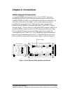
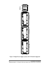
    Sdaibb1300 manual 3 b&b electronics mfg co inc – 707 dayton rd - po box 1040 - ottawa il 61350 - ph 815-433-5100 - fax 815-433-5104 chapter 2: connections power supply connections a single sdaibb board requires 8 ma at 10 to 30 vdc, and can be brought directly into the board through terminal blocks ...

  • Page 6

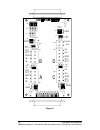
    4 sdaibb1300 manual b&b electronics mfg co inc – 707 dayton rd - po box 1040 - ottawa il 61350 - ph 815-433-5100 - fax 815-433-5104 j p 2 board 2 j p 9 j p 1 0 22.28/user 1 j p 1 1 gain j p 4 r 8 1 j p 8 22.28/ user out. Off. 2.5v 0v t b 1 out off g n d in+ in- out off g n d in+ in- gain j p 6 r 2 t...

  • Page 7: Input Voltage Connections

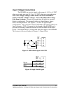
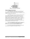
    Sdaibb1300 manual 5 b&b electronics mfg co inc – 707 dayton rd - po box 1040 - ottawa il 61350 - ph 815-433-5100 - fax 815-433-5104 input voltage connections the sdaibb can receive signals in the range of –0.15 to +5 vdc when set to unity gain, and –0.15 to +3.5 vdc when set to any other gain. Note:...

  • Page 8: Output Voltage Connections

    6 sdaibb1300 manual b&b electronics mfg co inc – 707 dayton rd - po box 1040 - ottawa il 61350 - ph 815-433-5100 - fax 815-433-5104 output voltage connections the sdaibb outputs voltages from +0.1 to +5.0 vdc at unity gain, and +0.1 to +4.95 vdc at any other gain. All lines are carried straight thro...

  • Page 9

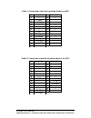
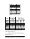
    Sdaibb1300 manual 7 b&b electronics mfg co inc – 707 dayton rd - po box 1040 - ottawa il 61350 - ph 815-433-5100 - fax 815-433-5104 table 1: connections when the 4-position shunt is on jp9 pin connection pin connection 1 --- 14 --- 2 power 15 --- 3 --- 16 --- 4 --- 17 --- 5 --- 18 --- 6 --- 19 --- 7...

  • Page 10

    8 sdaibb1300 manual b&b electronics mfg co inc – 707 dayton rd - po box 1040 - ottawa il 61350 - ph 815-433-5100 - fax 815-433-5104 to support all 11 channels on the sdaxx modules connect 3 sdaibbs to the i/o port of the sdaxx as shown in figure 2 on page 4 and set one board to jp9, one to jp10, and...

  • Page 11: Chapter 3: Configuration

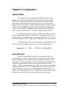
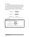
    Sdaibb1300 manual 9 b&b electronics mfg co inc – 707 dayton rd - po box 1040 - ottawa il 61350 - ph 815-433-5100 - fax 815-433-5104 chapter 3: configuration output offset the output offset is the amount by which the output is shifted. Equation 1 shows how the output offset affects the output of the ...

  • Page 12

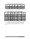
    10 sdaibb1300 manual b&b electronics mfg co inc – 707 dayton rd - po box 1040 - ottawa il 61350 - ph 815-433-5100 - fax 815-433-5104 change r1 to change the gain on channel a, r2 to change channel b, r7 to change channel c, and r8 to change channel d. The following sections explain how to calculate ...

  • Page 13

    Sdaibb1300 manual 11 b&b electronics mfg co inc – 707 dayton rd - po box 1040 - ottawa il 61350 - ph 815-433-5100 - fax 815-433-5104 maximum gain the maximum gain for a known differential voltage and common mode voltage can easily be determined using the following set of equations. Equation 5 calcul...

  • Page 14

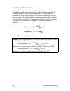
    12 sdaibb1300 manual b&b electronics mfg co inc – 707 dayton rd - po box 1040 - ottawa il 61350 - ph 815-433-5100 - fax 815-433-5104 gain resistor determination replacing a single resistor changes the gain on each buffer. Change r1 to modify the gain on channel a, r2 to change channel b, r7 to chang...

  • Page 15

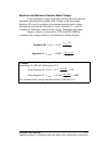
    Sdaibb1300 manual 13 b&b electronics mfg co inc – 707 dayton rd - po box 1040 - ottawa il 61350 - ph 815-433-5100 - fax 815-433-5104 maximum and minimum common mode voltage if the differential voltage range and desired gain are known, the maximum and minimum common mode voltage can be determined. Eq...

  • Page 16

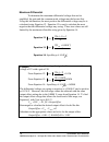
    14 sdaibb1300 manual b&b electronics mfg co inc – 707 dayton rd - po box 1040 - ottawa il 61350 - ph 815-433-5100 - fax 815-433-5104 maximum differential to determine the maximum differential voltage that can be amplified, the gain and the common mode voltage must be known first. Using this informat...

  • Page 17

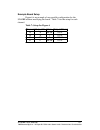
    Sdaibb1300 manual 15 b&b electronics mfg co inc – 707 dayton rd - po box 1040 - ottawa il 61350 - ph 815-433-5100 - fax 815-433-5104 example board setup figure 6 is an example of one possible configuration for the sdaibb without modifying the board. Table 7 lists the setup for each channel. Table 7:...

  • Page 18

    16 sdaibb1300 manual b&b electronics mfg co inc – 707 dayton rd - po box 1040 - ottawa il 61350 - ph 815-433-5100 - fax 815-433-5104 figure 6 c a d b out. Off. 2.5v 0 v g a i n 1 22.28/ u s e r o u t o f f g n d in+ in- o u t o f f g n d in+ in- 1 2 2 . 2 8 / u s e r g a i n o u t o f f g n d in+ in...

  • Page 19: Appendix A: Glossary

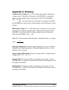
    Sdaibb3599 manual a-1 b&b electronics mfg co inc – 707 dayton rd - po box 1040 - ottawa il 61350 - ph 815-433-5100 - fax 815-433-5104 appendix a: glossary common mode voltage ( ) cm v : the voltage about which a differential voltage swings. When this is measured on the sdaibb it is calculated with a...

  • Page 20: Important Specs @ 25°C:

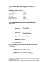
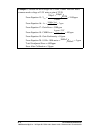
    Sdaibb3599 manual b-1 b&b electronics mfg co inc – 707 dayton rd - po box 1040 - ottawa il 61350 - ph 815-433-5100 - fax 815-433-5104 appendix b: error budget calculations important specs @ 25°c: v offset in ( ) osi v 200 µ v v offset out ( ) oso v 1000 µ v i offset ( ) os i 2na gain error 0.35% gai...

  • Page 21

    B-2 sdaibb3599manual b&b electronics mfg co inc – 707 dayton rd - po box 1040 - ottawa il 61350 - ph 815-433-5100 - fax 815-433-5104 example: calculate the error budget for a 350 Ω , 100mv load cell with a common mode voltage of 2.5v using a gain of 22.28. From equation 15: ppm mv v v v os 2449 100 ...

  • Page 22

    Fcc class a equipment statement federal communications commission radio frequency interface statement class a equipment this equipment has been tested and found to comply with the limits for class a digital device, pursuant to part 15 of the fcc rules. These limits are designed to provide reasonable...