- DL manuals
- Cadence
- Software
- PSPICE SCHEMATIC
- User Manual
Cadence PSPICE SCHEMATIC User Manual
Summary of PSPICE SCHEMATIC
Page 1
Pspice schematics schematic capture software user’s guide.
Page 2
Cadence pcb systems division 13221 sw 68th parkway, suite 200 portland, or 97223 copyright © 1985-2000 cadence design systems, inc. All rights reserved. Trademarks allegro, ambit, buildgates, cadence, cadence logo, concept, diva, dracula, gate ensemble, nc verilog, openbook online documentation libr...
Page 3: Contents
Contents before you begin xv welcome . . . . . . . . . . . . . . . . . . . . . . . . . . . . . . . . . . . . . Xv how to use this guide . . . . . . . . . . . . . . . . . . . . . . . . . . . . . Xvii symbols and conventions . . . . . . . . . . . . . . . . . . . . . . . . Xvii related documentation . ...
Page 4: Chapter 3
Contents iv using the schematic editor 27 chapter 3 overview . . . . . . . . . . . . . . . . . . . . . . . . . . . . . . . . . . . . 27 components of a design . . . . . . . . . . . . . . . . . . . . . . . . . . . . 29 parts . . . . . . . . . . . . . . . . . . . . . . . . . . . . . . . . . . . . . 29...
Page 5
Contents v opening a file . . . . . . . . . . . . . . . . . . . . . . . . . . . . . . . . 79 finding parts . . . . . . . . . . . . . . . . . . . . . . . . . . . . . . . . . . . 80 getting parts by name . . . . . . . . . . . . . . . . . . . . . . . . . . . 81 searching for parts in the libraries . . ...
Page 6: Chapter 5
Contents vi printing your design . . . . . . . . . . . . . . . . . . . . . . . . . . . . . 140 scaling . . . . . . . . . . . . . . . . . . . . . . . . . . . . . . . . . . . . 141 closing the schematic editor . . . . . . . . . . . . . . . . . . . . . . . . . 146 using the symbol editor 147 chapter 5 ...
Page 7: Chapter 7
Contents vii making a copy of a symbol . . . . . . . . . . . . . . . . . . . . . . . 173 importing a symbol definition . . . . . . . . . . . . . . . . . . . . . . 174 using ako symbols . . . . . . . . . . . . . . . . . . . . . . . . . . . 175 drawing symbol graphics . . . . . . . . . . . . . . . . ....
Page 8: Chapter 8
Contents viii setting up multiple views . . . . . . . . . . . . . . . . . . . . . . . . . . 237 translators . . . . . . . . . . . . . . . . . . . . . . . . . . . . . . . . . 237 navigating through hierarchical designs . . . . . . . . . . . . . . . . . 239 assigning instance-specific part values . . ...
Page 9: Exporting Dxf Files 301
Contents ix setting package class priorities . . . . . . . . . . . . . . . . . . . . . 284 generating a bill of materials report . . . . . . . . . . . . . . . . . . . . 286 printing and saving the report . . . . . . . . . . . . . . . . . . . . . 287 customizing the format of the report . . . . . . ....
Page 10: Glossary 331
Contents x glossary 331 index 337.
Page 11: Figures
Figures figure 1 interaction of sim software programs and files . . . . . . . . . . . . . . . 3 figure 2 opto-isolated, addressable serial-to-parallel converter circuit . . . . . . 5 figure 3 border styles . . . . . . . . . . . . . . . . . . . . . . . . . . . . . . . . . . . 50 figure 4 placing resi...
Page 12
Figures xii.
Page 13: Tables
Tables table 1 remaining parts to be placed . . . . . . . . . . . . . . . . . . . . . . . . . . 10 table 2 standard schematics toolbar . . . . . . . . . . . . . . . . . . . . . . . . . . 33 table 3 drawing toolbar . . . . . . . . . . . . . . . . . . . . . . . . . . . . . . . . . 35 table 4 simulatio...
Page 15: Before You Begin
Before you begin welcome orcad family products offer a total solution for your core design tasks: schematic- and vhdl-based design entry; fpga and cpld design synthesis; digital, analog, and mixed-signal simulation; and printed circuit board layout. What's more, orcad family products are a suite of ...
Page 16
Chapter before you begin 16 • graphically characterize simulation stimuli using the fully integrated pspice stimulus editor, so stimulus definitions are automatically associated with the appropriate symbols • graphically characterize simulation models using the fully integrated pspice model editor u...
Page 17: How to Use This Guide
How to use this guide 17 how to use this guide this guide is designed so you can quickly find the information you need to use pspice schematics. To help you learn and use pspice schematics efficiently, this manual is separated into the following sections: • chapter 1 - getting started • chapter 2 - ...
Page 18
Chapter before you begin 18 related documentation in addition to this guide, you can find technical product information in the online help, online books, and our technical web site, as well as in other books. The table below describes the types of technical documentation provided with pspice schemat...
Page 19
How to use this guide 19 orcad family customer support at www.Orcad.Com/technical/technical.Asp an internet-based support service available to customers with current support options. A few of the technical solutions within the customer support area are: • the knowledge base, which is a searchable da...
Page 20
Chapter before you begin 20
Page 21: Getting Started
Getting started 1 overview this chapter describes schematics: what it is, what it can do, and how you can use it. This chapter has the following sections: using schematics on page 1-2 provides a broad overview and describes various functions. Example—drawing a schematic on page 1-4 provides a step-b...
Page 22: Using Schematics
Chapter 1 getting started 2 using schematics schematics is a schematic capture front-end program that provides a convenient system for: • creating and managing circuit drawings. • setting up and running simulations. • evaluating simulation results using microsim probe. • creating netlists for extern...
Page 23
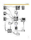
Using schematics 3 figure 1 interaction of sim software programs and files packages symbols models pcb layout footprints layout eco file layout netlist file pspice schematics probe circuit file component description file bill of materials reports pspice a/d probe data file simulation output file sim...
Page 24
Chapter 1 getting started 4 example—drawing a schematic the following example demonstrates the basic drawing features for drawing a schematic. It shows you how to: • start the schematic editor and begin a new design. • find out which libraries are configured for schematics. • place parts on a schema...
Page 25
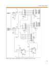
Example—drawing a schematic 5 figure 2 opto-isolated, addressable serial-to-parallel converter circuit.
Page 26
Chapter 1 getting started 6 starting a new design start the schematic editor by double-clicking on the schematics icon in the orcad program group. An empty schematic page displays. If you already have schematics running with another schematic displayed, click the new file icon to start a new schemat...
Page 27
Example—drawing a schematic 7 checking symbol libraries configuration when you installed schematics, you selected a set of libraries to be installed. These are global libraries, which means the symbols contained in them are available to be used in any new or existing schematic. Check to see that you...
Page 28
Chapter 1 getting started 8 selecting and placing parts 1 from the draw menu, select get new part to display the part browser dialog box. 2 there are several ways to select a part in the part browser dialog box: • if you know the name of the part, type the name in the part name text box. • select th...
Page 29
Example—drawing a schematic 9 placing resistors r1 and r2 1 from the draw menu, select get new part to display the part browser dialog box (shown on 1-8 ). 2 type r in the part name text box. 3 click place & close. The outline of the resistor becomes attached to the pointer. Note that as you move th...
Page 30
Chapter 1 getting started 10 3 place the pointer in the approximate position for the placement of r3 and click to place the part. 4 press m three times to place three more resistors above the first. Placing resistors r7 through r10 1 from the get recent part list box on the toolbar, select r . 2 pre...
Page 31
Example—drawing a schematic 11 drawing and labeling wires draw the wire labeled dataclk to connect pin 8 (clk) on u3 and pin 1 (a) on u8a. Drawing the dataclk wire 1 click the draw wire button. The pencil pointer indicates that you are ready to draw a wire. 2 click pin 8 of u3 to begin the wire. 3 f...
Page 32
Chapter 1 getting started 12 drawing and labeling buses draw the bus labeled db[1-12]. Drawing the bus 1 click the draw bus button. The pointer is now shaped like a pencil (as it was when you were drawing wires). 2 click where you want to start the bus. 3 click the pointer where you want to end the ...
Page 33
Example—drawing a schematic 13 labeling the wires connected to the bus you can use auto-naming to label a uniform collection of wires. 1 from the options menu, select auto-naming to display the auto naming dialog box. A in the wire/port labels frame, select the enable auto-increment check box. B in ...
Page 34
Chapter 1 getting started 14 changing reference designators and part values change part values and reference designators by double-clicking them and typing a new value in the dialog box. Changing u8a to u9b 1 double-click u8a to display the edit reference designator dialog box. 2 type u9 in the pack...
Page 35
Example—drawing a schematic 15 moving parts, wires, and text move parts, wires, buses, and text by clicking to select them, and dragging them to a new location. To maintain connectivity when moving parts, wires, or buses, enable the rubberbanding option. Moving resistor r1 up one grid 1 click the re...
Page 36
Chapter 1 getting started 16 placing ports ports in schematics identify signals that are inputs or outputs to a schematic. Place ports in the same way that you place other parts. Placing the port 1 from the draw menu, select get new part to display the part browser dialog box (shown on page 8). 2 cl...
Page 37
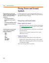
Example—drawing a schematic 17 labeling the port 1 double-click the port symbol to display the set attribute value dialog box. 2 type dat in the label text box. 3 click ok. Now place two more ports and label them clk and rtn as shown in figure 2. Placing power and ground symbols power and ground sym...
Page 38
Chapter 1 getting started 18 placing ground symbols 1 in the get recent part list box on the toolbar, type egnd . 2 press r to select the part. 3 move the pointer to the location of the ground symbol and click to place the symbol. 4 move the pointer and click to place the other four ground symbols. ...
Page 39: Using Design Manager
Using design manager 2 overview this chapter provides introductory information about the design manager. This chapter has the following sections: understanding design manager on page 2-20 describes the purpose and uses for design manager. Managing your files in the workspace on page 2-22 explains wh...
Page 40: Understanding Design Manager
Chapter 2 using design manager 20 understanding design manager design manager allows you to browse, manage, archive, and restore your design files. When you open a design file, design manager searches the windows explorer for the following information: • the name of the top-level folder where the fi...
Page 41
Understanding design manager 21.
Page 42: Managing Your Files In The
Chapter 2 using design manager 22 managing your files in the workspace design manager views a file’s top-level folder (as seen in windows explorer) as a workspace and assigns it the name of the top-level folder. Although workspaces are actual folders, categories are not. Categories only display file...
Page 43: Design Manager Functions
Design manager functions 23 design manager functions the following describes design manager functions and activities: general characteristics • availability for use without other orcad programs running • automatic categorization of design-related files, sorted into file-type categories, within a wor...
Page 44
Chapter 2 using design manager 24 archive and restore • archive and restore to save a design and all of its references, package files for shipment to another location, save disk space, and localize externally referenced and shared files into a selected workspace.
Page 45: Starting The Design Manager
Starting the design manager 25 starting the design manager the design manager is automatically opened and minimized when you open pspice schematics. You can also open design manager to view and manage files without first opening schematics. Opening the design manager outside of schematics 1 on the t...
Page 46
Chapter 2 using design manager 26.
Page 47: Using The Schematic Editor
Using the schematic editor 3 overview this chapter provides background information about the schematic editor. To see specific step-by-step instructions for creating a design, see chapter 4, creating and editing designs . This chapter has the following sections: components of a design on page 3-29 i...
Page 48
Chapter 3 using the schematic editor 28 of your schematic, in addition to specifying colors and sizes. Zooming and panning in schematics on page 3-68 tells how to zoom in and out of the drawing, refresh the screen display, pan to various sections of the drawing and fit the drawing to the page. Using...
Page 49: Components of A Design
Components of a design 29 components of a design a schematic consists of: • symbols • attributes • wires • buses • text items schematics can have either a flat or hierarchical structure, depending on the way you decide to implement your design. Parts parts are electrical devices that make up a circu...
Page 50
Chapter 3 using the schematic editor 30 symbols symbols are the graphical representation of parts, ports, and other schematic elements. They are grouped by functionality into symbol libraries. Each symbol contains a specific set of attributes that define the symbol. You can edit these attributes as ...
Page 51
Components of a design 31 connections parts and ports contain one or more pins where connections are made. Electrical connections are formed by wire and bus segments joining pins and other wire and bus segments. Connections are also formed by attaching pins directly to pins. Pspice schematics repres...
Page 52: Main Window
Chapter 3 using the schematic editor 32 main window when you start pspice schematics, a schematic editor window opens and displays a single schematic page. You have the option of opening additional schematic editor windows. Use these windows to: • display different schematics. • display different po...
Page 53
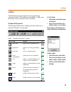
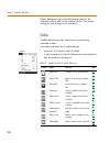
Main window 33 toolbars toolbar buttons provide shortcuts for performing common actions. All toolbars are dockable, so they may be moved to any location on the schematic. Standard schematics the standard schematics toolbar provides shortcuts to standard windows commands. Table 2 standard schematics ...
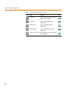
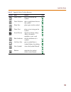
Page 54
Chapter 3 using the schematic editor 34 redraw refreshes the active schematic page screen display 3-41 zoom in views a smaller area of schematic 3-68 zoom out views a larger area of schematic 3-69 zoom area views a selected area of schematic 3-68 zoom to fit page fits the view to show all items on t...
Page 55
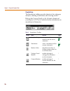
Main window 35 drawing the drawing toolbar provides shortcuts for drawing and editing items on your schematic. Table 3 drawing toolbar button name function page draw wire enables drawing of wires on the schematic 4-10 4 draw bus enables the drawing of buses on the schematic 4-10 7 draw block enables...
Page 56
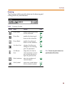
Chapter 3 using the schematic editor 36 simulation the simulation toolbar provides shortcuts for setting up analyses, running a simulation, and viewing results. Refer to the viewing results on the schematic chapter of your pspice a/d user’s guide for further information on simulation in schematics. ...
Page 57
Main window 37 enable bias voltage display toggles the display of bias voltage * show/hide voltage on selected net(s) toggles the display of voltages for selected wires * enable bias current display toggles the display of bias current * show/hide currents on selected part(s) toggles the display of c...
Page 58
Chapter 3 using the schematic editor 38 annotation graphics the annotation graphics toolbar provides shortcuts for drawing or inserting non-electrical information onto your schematic. Table 5 annotation graphics toolbar button name function page draw arc draws an arc shape on the page 6-17 8 draw bo...
Page 59
Main window 39 status bar the status bar is located at the bottom of the schematic editor window and provides the following: • x and y coordinates of the pointer. Use the display options selection under the options menu to toggle display of x and y coordinates. • a message area that provides: • a br...
Page 60
Chapter 3 using the schematic editor 40 table 6 schematic editor function keys key action menu selection 1 online help help help 2 move to lower level in the schematic hierarchy navigate push 3 move up one level in the schematic hierarchy navigate pop 4 text stay-on-grid options display options 5 or...
Page 61
Configuring pspice schematics 41 configuring pspice schematics the following list summarizes the different types of options you can configure in pspice schematics. Customizing configurable options allows you to use pspice schematics in the way that best suits your needs and requirements. Library set...
Page 62
Chapter 3 using the schematic editor 42 configuring symbol libraries there are two major elements that work together in schematics that let you place symbols into your design: • symbol libraries • library search list symbol libraries are located in library directories. The library search list is in ...
Page 63
Configuring pspice schematics 43 types of libraries schematics recognizes two types of libraries: default library directory schematics includes a default library directory where all the symbol libraries (. Slb ) you selected during installation reside. It is not required to configure these libraries...
Page 64
Chapter 3 using the schematic editor 44 user-defined symbol libraries you can create global and local symbol libraries, and add them to the default directory or to another directory of your choice. Once created, you can perform all the same actions as listed in default library directory on page 3-43...
Page 65
Configuring pspice schematics 45 3 in the list of libraries, select the location for the new library. A new global library will be added directly above the library you select. A new local library will be placed above the first global library name in the list. 4 if the library you are adding is a sym...
Page 66
Chapter 3 using the schematic editor 46 removing library names if you no longer need a library name in the list of configured libraries, you can remove it from the list of configured libraries. Removing a library name 1 from the options menu, select editor configuration to display the editor configu...
Page 67
Configuring pspice schematics 47 do not type a file name extension; the file name extension is appended automatically. 5 click change. 6 click ok to exit the library setting dialog box. 7 in the editor configuration dialog box, click ok. Changing the search order the way that pspice schematics searc...
Page 68
Chapter 3 using the schematic editor 48 the repositioned library name is inserted above the selected name. 9 click ok to exit the library setting dialog box. 10 in the editor configuration dialog box, click ok. Changing the search path pspice schematics looks for a library according to the path(s) s...
Page 69
Configuring pspice schematics 49 changing page size pspice schematics supports standard page sizes a through e and a0 through a4. It also allows you to specify a user defined page size. Changing the page size 1 from the options menu, click page size to display the page size dialog box. 2 click the a...
Page 70
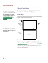
Chapter 3 using the schematic editor 50 changing page settings for all page sizes, you can change the border style, the drawing area, and the pin-to-pin spacing. Border style schematics provides two border styles: zoned and outline. Figure 3 illustrates the two styles. Figure 3 border styles you can...
Page 71
Configuring pspice schematics 51 the following table lists the default metric page sizes and their configurations. Note if your design doesn’t require a zoned border, outline border will display the page with fewer details. Table 7 zoned border default decimal parameters type dimension* * in inches ...
Page 72
Chapter 3 using the schematic editor 52 changing the border style you can specify which border style to use through the editor configuration dialog box. The current drawing and all subsequent new drawings use the style you select. 1 from the options menu, select editor configuration to display the e...
Page 73
Configuring pspice schematics 53 4 select the outline or zoned border style. Note line widths for the page boundary are specified in the display preferences dialog box. See setting the default graphics properties through display preferences on page 4-132 for more information. For style... Do this......
Page 74
Chapter 3 using the schematic editor 54 drawing area changing the drawing area size 1 from the options menu, select editor configuration to display the editor configuration dialog box (shown on 3-52 ). 2 click page settings to display the page settings dialog box. 3 in the width and height text boxe...
Page 75
Configuring pspice schematics 55 pin-to-pin spacing you can scale symbols so they will appear larger or smaller on the schematic. You do this by changing the pin-to-pin spacing for a given page size. Changing the pin-to-pin spacing 1 from the options menu, select editor configuration to display the ...
Page 76
Chapter 3 using the schematic editor 56 stay-on-grid stay-on-grid controls the method of object placement. When stay-on-grid is enabled, the objects are forced onto grid when placed. We recommend that you enable this so that electrical connections are made correctly. Enabling or disabling stay-on-gr...
Page 77
Configuring pspice schematics 57 snap-to-pin snap-to-pin, when enabled, causes the endpoint of a wire or bus segment to snap to the nearest pin if one is found inside the radius defined by the gravity setting. Enabling or disabling snap-to-pin 1 from the options menu, select display options. 2 selec...
Page 78
Chapter 3 using the schematic editor 58 text grid text grid allows you to set the grid spacing for text separately from the drawing grid spacing. The text grid is usually set to some smaller percentage of the drawing grid. This allows you to align text between drawing grid points. Enabling text grid...
Page 79
Configuring pspice schematics 59 when autosave is enabled, pspice schematics creates a temporary file with the same name as the active working file, and a file name extension ending in ‘ v ’ (for example, “.Scv,” “.Slv,” “.Plv”). If you have a power outage or system failure, you can retrieve your wo...
Page 80: Schematics
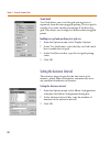
Chapter 3 using the schematic editor 60 controlling the display in pspice schematics pspice schematics allows you to define what elements of a design you want to display and print. This means you can set different display properties for each element of your schematic. In the display preferences dial...
Page 81
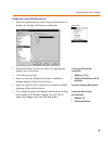
Controlling the display in pspice schematics 61 displaying or printing default properties 1 from the options menu, select display preferences to display the display preferences dialog box. 2 from the display layers list, select the appropriate display layer (or layers). 3 click the general tab. 4 se...
Page 82
Chapter 3 using the schematic editor 62 changing fonts to change the default fonts pspice schematics uses to display and print text, use the display preferences dialog box. Selecting a font 1 from the options menu, select display preferences to display the display preferences dialog box. 2 select on...
Page 83
Controlling the display in pspice schematics 63 5 select a font and size from their corresponding list boxes and click ok. A sample of the selected font is shown in the sample box. 6 enter a size in either inches or millimeters, or accept the system default for the selected font. 7 select a color fr...
Page 84
Chapter 3 using the schematic editor 64 changing application settings you have the option to change the location of the .Exe files of the programs that schematics interfaces with. You can also configure a different text editor (besides wordpad) and specify an initialization file other than the insta...
Page 85
Controlling the display in pspice schematics 65 the simulate command frame shows the path that pspice schematics uses to run microsim pspice a/d. 3 to change the path name, type a new path name in the command text box. 4 similarly, to change any of the other command lines, click to select the comman...
Page 86
Chapter 3 using the schematic editor 66 4 type the file name of the configuration file in the text box. 5 click ok to exit the app setting dialog box. 6 in the editor configuration dialog box, click ok. Specifying a different text editor editing text in pspice schematics is done through the wordpad ...
Page 87
Controlling the display in pspice schematics 67 changing the get recent part list size the get recent part list box on the toolbar contains a scroll-down list of recently placed parts. The default length of this list is ten items. To change the length of the list, use a text editor to edit the mrpli...
Page 88: Zooming and Panning In
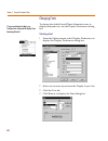
Chapter 3 using the schematic editor 68 zooming and panning in schematics zooming when working on a design, you can zoom in (enlarge the view) or zoom out (reduce the view) to view a larger or smaller portion of the schematic window. Zooming in reduces the area viewed and enlarges the objects viewed...
Page 89
Zooming and panning in schematics 69 zooming out about the center of the window 1 click the zoom out button. The amount of reduction is determined by the zoom scale factor (see setting zoom parameters on page 3-69 ). Zooming out to view the full schematic page 1 from the view menu, select entire pag...
Page 90
Chapter 3 using the schematic editor 70 this value defines the percentage of the work space to be filled with the complete schematic when you select view fit. Type a decimal value between 50 and 100. A typical value is 90. 4 click ok. Fitting to a page all of the parts, wires and text within the act...
Page 91
Zooming and panning in schematics 71 automatic panning if auto pan is enabled, the pointer turns to a solid black arrow when you move it to the edge of the window. If you leave the arrow at the edge of the window for a few moments, the view pans in the direction of the arrow. You can pan up, down, l...
Page 92
Chapter 3 using the schematic editor 72 setting auto pan sensitivity the auto pan sensitivity setting determines how long the pointer must remain on the window border before the panning takes place. 1 from the options menu, click pan & zoom to display the pan & zoom dialog box (shown on page 3-71 )....
Page 93: Using The Message Viewer
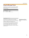
Using the message viewer 73 using the message viewer the message viewer displays text describing a condition, status or other information concerning the operation of pspice schematics. The message viewer appears when any condition generates a message that requires you to be informed. For example, wa...
Page 94
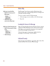
Chapter 3 using the schematic editor 74 online help the message viewer has an online help feature that allows you to view a help message directly relating to the currently selected message. To view a context-sensitive help message: 1 in the message viewer window, select the message. 2 press 1. Locat...
Page 95
Using the message viewer 75 table 1: color indication blue informational message. No user action is required. Yellow warning message. May require some user action. Red error message. Must be corrected before continuing. Black fatal error message. Indicates a non-recoverable error condition..
Page 96
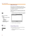
Chapter 3 using the schematic editor 76 additional information some messages contain additional text. That is, the message contains several lines of information while only one line displays. Lines containing additional information are indicated by a plus sign in the severity marker preceding the mes...
Page 97: Overview
Creating and editing designs 4 overview this chapter contains the step-by-step procedures for creating, editing, and printing a schematic, which includes: starting the schematic editor on page 4-79 describes how to start the schematic editor and how to open a new or existing file. Finding parts on p...
Page 98
Chapter 4 creating and editing designs 78 using wires and buses on page 4-104 describes drawing and labeling wires and buses, in addition to describing the drawing options that affect the placement of wires and buses. Using ports on page 4-114 describes the use of off-page and global ports. Selectin...
Page 99
Starting the schematic editor 79 starting the schematic editor start the schematic editor by double-clicking on the schematics icon in the orcad program group. An empty schematic page appears. If you already have schematics running with another schematic open, click the new file button to start a ne...
Page 100: Finding Parts
Chapter 4 creating and editing designs 80 finding parts parts represent electrical devices such as resistors, operational amplifiers, diodes, voltage sources, and digital gates that comprise the circuit diagram. The graphical representation of a part is a symbol stored in a symbol library. For those...
Page 101
Finding parts 81 getting parts by name the get recent part list box on the toolbar provides a list of the most recently used parts. You can also type a name in the get recent part list box to select a part. Selecting a part by name 1 in the get recent part list box, type the name of the part you wan...
Page 102
Chapter 4 creating and editing designs 82 searching for parts in the libraries symbol libraries contain symbols for many parts. There are three methods for selecting parts from libraries: • search for the part by name. • search for the part by description. • browse through the symbol libraries. Each...
Page 103
Finding parts 83 4 move the outline of the selected symbol to any location on the schematic and click to place the part. 5 right-click to stop placing parts. Selecting a part by description 1 click the get new part button to display the part browser dialog box (see 4-82 ). Note you may display one o...
Page 104
Chapter 4 creating and editing designs 84 7 move the outline of the selected symbol to any location on the schematic and click to place the part. 8 right-click to stop placing parts. Browsing symbol libraries to select a part 1 click the get new part button to display the part browser dialog box (se...
Page 105: Placing And Editing Parts
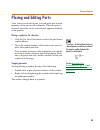
Placing and editing parts 85 placing and editing parts after you have selected a part, you can place one or more instances of the part on the schematic. When the part is selected, an outline of the selected part appears attached to the pointer. Placing a symbol on the schematic 1 click the get new p...
Page 106
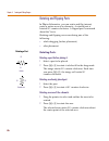
Chapter 4 creating and editing designs 86 rotating and flipping parts in pspice schematics, you can rotate and flip (mirror) parts or entire areas of a schematic. A rotated part is rotated 90° counter-clockwise. A flipped part is mirrored about the y axis. Rotating and flipping can occur during one ...
Page 107
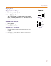
Placing and editing parts 87 flipping parts flipping a part before placing it 1 select the part to be placed. 2 press c+f to flip it. The symbol outline is a mirror image of the original image. Each time you press c+f, the image will flip about the vertical axis. Flipping an already placed part 1 se...
Page 108
Chapter 4 creating and editing designs 88 editing part attributes parts, ports, wires (nets), buses and most other symbols have associated attributes. An attribute consists of a name and an associated value. (see attributes on page 3-30 .) you can create new attributes or edit existing attributes of...
Page 109
Placing and editing parts 89 the letter a indicates that the attribute has been annotated as a result of back annotation or has been assigned by the packager. Any changes you make to the part attributes are made to the individual part instance you selected. The original part contained in the symbol ...
Page 110
Chapter 4 creating and editing designs 90 adding attributes adding a new attribute 1 double-click the part to display the attribute editing dialog box (see 4-88 ). 2 double-click in the name text box and type the new attribute name. 3 press f and type the new attribute value in the value text box. 4...
Page 111
Placing and editing parts 91 3 click change display to display the change attribute dialog box. 4 select one of the option buttons in the what to display frame. With many attributes such as the package reference and reference designator, only the value displays. With others, such as package type, ne...
Page 112
Chapter 4 creating and editing designs 92 4 select or type a value for any of the display characteristics. You can change any of the characteristics as described in table 9 . 5 click ok to close the change attribute dialog box. 6 click ok to close the attribute editing dialog box. This procedure onl...
Page 113
Placing and editing parts 93 global editing of attributes pspice schematics allows you to change an attribute on multiple parts at the same time. Assigning the same attribute value to multiple parts 1 select more than one part, or select an area of the drawing enclosing the parts. 2 select the edit ...
Page 114
Chapter 4 creating and editing designs 94 editing the default attributes of a symbol when placing parts, you might want to change the value of an attribute for all parts of a certain type, such as a resistor. For example, you might want to change the default value for all resistors being placed from...
Page 115
Placing and editing parts 95 11 type a name in the file name text box. 12 click save. You are prompted to add the library to the list of configured libraries. 13 click yes. Repeating part placements if you are placing parts in line with each other and evenly spaced, use the auto-repeat function. Aut...
Page 116
Chapter 4 creating and editing designs 96 4 select the part from the symbol library. 5 place the first instance of the part. 6 press m once to place each subsequent instance of the same part. Manually repeating part placements 1 if auto-repeat is not enabled, press m to repeat the last action. If th...
Page 117
Placing and editing parts 97 • right-click to stop placing the part without placing an additional part. The outline changes back to a pointer. Automatically assigning reference designators the auto naming function is useful for assigning reference designators to parts as they are placed. The default...
Page 118
Chapter 4 creating and editing designs 98 example—using auto-repeat and auto naming use the following procedure to create part of the drawing shown in figure 5 using the auto-repeat and auto naming functions. Placing the bus and part 1 click the draw bus button. 2 move the pencil-shaped pointer to t...
Page 119
Placing and editing parts 99 drawing the first wire segment connecting the part to the bus 1 click the draw wire button. 2 move the pencil-shaped pointer to a point on the bus where wire segment a[0] attaches to the bus. Click to start drawing the wire. 3 move to pin d1 on u1 and double-click. Using...
Page 120
Chapter 4 creating and editing designs 100 replacing parts a single part on a schematic may be replaced easily. In addition, all parts of a given type on a page, or all pages of a multi-page design may be replaced. Instead of having to delete one part, find another in a library, and place the new pa...
Page 121
Placing and editing parts 101 replacing all parts of the same name 1 from the edit menu, select replace to display the replace part dialog box. 2 in the target part text box, type the name of the parts to be replaced. 3 in the replacement text box, type the name of the replacement parts. 4 if you wa...
Page 122: Placing Power And Ground
Chapter 4 creating and editing designs 102 placing power and ground symbols in pspice schematics, power and ground symbols are a type of global port symbol. The label on the port defines the name of the power supply. Placing power and ground symbols placing a symbol on the schematic 1 from the draw ...
Page 123
Placing power and ground symbols 103 creating custom power and ground symbols because power and ground symbols are just like any other symbols, you can use the symbol editor to create your own custom power and ground symbols. See drawing symbol graphics on page 6-178 ..
Page 124: Using Wires and Buses
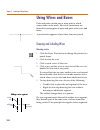
Chapter 4 creating and editing designs 104 using wires and buses parts and ports contain one or more pins to which connections can be made. Electrical connections are formed by joining pins of parts and ports with wires and buses. A junction dot appears where three items are joined. Drawing and labe...
Page 125
Using wires and buses 105 if a wire segment is added so its end-point intersects another wire segment (at a point other than its end-points), a junction is created and the original wire is split into two segments. All three segments become part of the same wire. You can place a label on selected wir...
Page 126
Chapter 4 creating and editing designs 106 2 click the wire segment that you want to change. 3 click to place a vertex. 4 double-click to place the last vertex and stop rewiring. Drawing and labeling buses the connectivity of buses and bus segments in pspice schematics is controlled by labeling. The...
Page 127
Using wires and buses 107 drawing a bus 1 click the draw bus button to change the pointer to a pencil shape. 2 click to start the bus. 3 click at each vertex of the bus. 4 right-click to end the bus and change the pencil back to a pointer. Labeling a bus 1 double-click the bus segment to display the...
Page 128
Chapter 4 creating and editing designs 108 2 label the bus segment with a subset of the signals on the main bus. For example, you can label the bus segment db[0:8] if the main bus is labeled db[0:16]. Automatically labeling wires and buses use the auto naming function to set up the labeling of wires...
Page 129
Using wires and buses 109 specifying drawing options several options aid in drawing wires and buses and in placing parts. • the orthogonal option constrains wires and buses to vertical and horizontal lines. • the snap-to-grid option keeps parts, wires, and buses aligned to grid lines. • the snap-to-...
Page 130
Chapter 4 creating and editing designs 110 enabling orthogonal drawing 1 from the options menu, select display options. 2 in the options frame, select or clear the orthogonal check box to enable or disable orthogonality. 3 click ok. Snap-to-grid snap-to-grid controls the movement of the object while...
Page 131
Using wires and buses 111 gravity gravity specifies how close an object must be to a pin to snap to it. Gravity is only functional when snap-to-pin is enabled. Specifying gravity 1 from the options menu, select display options (shown on page 4-110 ). 2 in the snap-to-pin frame, in the gravity box, t...
Page 132
Chapter 4 creating and editing designs 112 figure 7 rubberbanding with orthogonal enabled figure 8 rubberbanding with orthogonal disabled.
Page 133
Using wires and buses 113 while you are moving an object (whether orthogonal is enabled or disabled), an x appears where a new connection will be made if the object is placed, and the pointer changes to a caution sign (see figure 9 below). If you continue to move the object (away from the connection...
Page 134: Using Ports
Chapter 4 creating and editing designs 114 using ports signals can be connected without using wires or buses by connecting them to global or off-page ports and labeling the ports with the same name. Off-page ports off-page ports connect to other off-page ports with the same name on the same page or ...
Page 135
Using ports 115 placing a global port 1 click the get new part button to display a part browser dialog box, (see 4-82 ). 2 click libraries to display the library browser dialog box (see 3-45 ). 3 in the library list, select port.Slb. 4 in the part list, double-click global. 5 click place to place th...
Page 136: Selecting and Moving Objects
Chapter 4 creating and editing designs 116 selecting and moving objects and attributes before performing any operation on a schematic object, you have to select the object. You can make multiple selections or select whole areas of the schematic. After you select an object, you can move, copy, delete...
Page 137
Selecting and moving objects and attributes 117 a rectangle is drawn around the attribute; a selection rectangle also appears around the object that the attribute belongs to. De-selecting selected objects 1 click to select an object other than the selected object, or click in a blank area of the sch...
Page 138
Chapter 4 creating and editing designs 118 finding a part 1 from the edit menu, select find to display the find dialog box. 2 specify the search criteria: a type an attribute name in the name text box. B type the attribute value in the value text box. C click add criterion to add the search criteria...
Page 139
Selecting and moving objects and attributes 119 cutting, copying, and pasting pspice schematics provides several editing features that allow you to cut, copy, paste, copy to clipboard, delete, and undelete selected objects. All of these functions are available under the edit menu. Most can be access...
Page 140
Chapter 4 creating and editing designs 120 pasting an object 1 from the edit menu, select paste to change the pointer to the shape of the object last cut or copied. 2 click to place the object at the current pointer location. Continue moving the pointer to various locations and clicking to place add...
Page 141
Selecting and moving objects and attributes 121 copying to the clipboard the copy to clipboard function copies objects within a selection rectangle to the microsoft windows clipboard for use in other windows programs. Electrical or connectivity information is not copied to the clipboard. This functi...
Page 142
Chapter 4 creating and editing designs 122 creating and editing title blocks each new schematic is created with a title block in the lower-right corner of the page. The title block is treated as an annotation symbol and each text field is an attribute. As such, you can edit the attributes of the tit...
Page 143
Creating and editing title blocks 123 entering information into the title block entering information into the existing title block can be done in one of two ways: (1) by editing the attributes of the title block, in which case you can type information into any, or all fields of the title block, or (...
Page 144
Chapter 4 creating and editing designs 124 editing one attribute of the title block 1 double-click the attribute of the title block to display the set attribute value dialog box. 2 type or correct the information in the text box. 3 click ok. Creating a custom title block because the title block is t...
Page 145
Creating and editing title blocks 125 using a custom title block symbol after you have created a custom title block, you have to specify that block in order to use it in the current schematic. Specifying a new title block symbol 1 from the options menu, select editor configuration to display the edi...
Page 146: Adding Non-Electrical
Chapter 4 creating and editing designs 126 adding non-electrical information non-electrical information such as comments, tables, and graphics can be added to the schematic. There are three types of non-electrical information: • text—multiple lines or a single line, such as comments or instructions ...
Page 147
Adding non-electrical information 127 resizing the text box 1 select the text box to display its handles. 2 click one of the handles and drag to resize the text box. Editing text 1 click inside the text box to modify or add text. Single line text editing with the single line text option, you can con...
Page 148
Chapter 4 creating and editing designs 128 • right-click to stop placing the text string without placing an additional one. The outline changes back to a pointer. Resizing the text box 1 select the text to display the text box handles. 2 click one of the handles and drag to resize the box to the siz...
Page 149
Adding non-electrical information 129 3 select the appropriate properties for the text selected. Note in addition to changing the text properties, you can change the properties of the text box itself in the frame area. 4 click ok. Setting the default text properties through display preferences 1 fro...
Page 150
Chapter 4 creating and editing designs 130 3 click the text tab. 4 select the appropriate properties. 5 click apply to apply the changes immediately and keep the dialog box open for further changes, or click ok to apply the changes and close the dialog box. Graphics adding graphics graphics can be a...
Page 151
Adding non-electrical information 131 resizing annotation graphics 1 select the object to display its handles. 2 click one of the handles and drag to resize the object. Changing graphics properties there are two ways to change the graphics properties in pspice schematics: • changing properties can b...
Page 152
Chapter 4 creating and editing designs 132 setting the default graphics properties through display preferences 1 from the options menu, select display preferences to display the display preferences dialog box (shown on 4-129 ). 2 from the display layers list, select the annotation graphics layer. 3 ...
Page 153
Adding non-electrical information 133 importing bitmaps and metafiles you can import bitmap (.Bmp, .Dib), windows metafiles (.Wmf), or enhanced metafiles (.Emf) onto the schematic. Importing a graphic 1 from the draw menu, select insert picture to display the open dialog box. 2 select the file type:...
Page 154
Chapter 4 creating and editing designs 134 annotation symbols creating annotation symbols and adding them to a custom library allows you to easily use them in other designs. Creating annotation symbols 1 from the edit menu, select symbol to start the symbol editor. 2 from the file menu, select open....
Page 155
Adding non-electrical information 135 a add any attributes to contain custom information for later use. B click ok. 6 from the file menu, select save. Moving non-electrical information moving text, graphics, and annotation symbols 1 select the object. 2 place the pointer on the edge of the object an...
Page 156: Designs
Chapter 4 creating and editing designs 136 creating and editing multi-sheet designs a schematic can contain one or more pages. As a schematic grows beyond a single page, ports are used to establish connectivity. Off-page ports provide connectivity between pages of the same schematic. Global ports pr...
Page 157
Creating and editing multi-sheet designs 137 copying a page 1 from the navigate menu, select copy page to display the copy page dialog box. 2 select the schematic file from the directory list. 3 select a page number, if the page to be copied is part of a multi-page schematic. 4 click ok to add the p...
Page 158
Chapter 4 creating and editing designs 138 viewing multiple pages to view pages in a multi-page design, use the previous page, next page, and select page selections under the navigate menu. Viewing the previous page 1 from the navigate menu, select previous page. Viewing the next page 1 from the nav...
Page 159
Creating and editing multi-sheet designs 139 deleting a page to delete a page from a multi-page design, use delete page under the navigate menu. Deleting a page 1 navigate to the page you want to delete. 2 from the navigate menu, select delete page to display a delete page confirmation dialog box. 3...
Page 160: Printing Your Design
Chapter 4 creating and editing designs 140 printing your design printing options allow you to print one or more pages, or a selected area of a schematic. Printing the current page of the current schematic 1 click the print button. The page is immediately sent to the current (default) printer. Printi...
Page 161
Printing your design 141 3 select one of the scaling options. See scaling on page 4-141 . 4 select an orientation of either landscape or portrait. Most schematics are in landscape format. Landscape is the schematic editor default format. 5 click ok. Scaling scaling options allow you to control the s...
Page 162
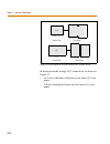
Chapter 4 creating and editing designs 142 user-definable zoom factor user-definable zoom factor allows you to set a custom zoom factor. For example, with the zoom factor set at 100%, a b-size schematic will print on two a-size sheets of paper when the printer is configured in portrait mode, as show...
Page 163
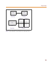
Printing your design 143 with the zoom factor set to 200%, a b-size drawing will print on eight sheets of paper as shown in figure 15. Doubling the zoom factor quadruples the number of printer pages needed to print a schematic. With user-definable zoom enabled, the printer configured in portrait mod...
Page 164
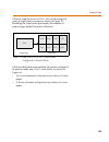
Chapter 4 creating and editing designs 144 in landscape mode, using a 100% zoom factor, as shown in figure 17: • an a-size schematic will print on one sheet of a-size paper. • a b-size drawing will print on four sheets of a-size paper. B-size 8 1/2 x 11 8 1/2 x 11 11 x 8 1/2 17 x 11 a-size figure 16...
Page 165
Printing your design 145 b-size 11x 8 1/2 schematic page a-size 11x 8 1/2 printed paper a-size figure 17 user-definable zoom enabled in landscape mode 17 x 11 11 x 8 1/2 11 x 8 1/2 11 x 8 1/2 11 x 8 1/2 schematic page printed paper.
Page 166: Closing The Schematic Editor
Chapter 4 creating and editing designs 146 closing the schematic editor you can close the schematic editor, thereby closing all open schematics. You can also close an open schematic without exiting the schematic editor. Closing the schematic editor to exit the schematic editor and close all currentl...
Page 167: Using The Symbol Editor
Using the symbol editor 5 overview the symbol editor enables you to do the following tasks: • create and edit symbols for use in the schematic editor • edit existing libraries • create new libraries this chapter provides background information about the symbol editor, which includes: starting the sy...
Page 168
Chapter 5 using the symbol editor 148 changing text characteristics on page 5-158 describes procedures for changing the text characteristics of attribute text, pin name and number display, and free-standing text. Changing grid and gravity on page 5-162 describes enabling and disabling grid, setting ...
Page 169: Components
Components 149 components a component or device has several aspects associated with it: • symbol—the graphical representation used in drawing schematics • packaging information—defines the names of the package types (footprints) in which the component is available, the pin number assignments for tho...
Page 170
Chapter 5 using the symbol editor 150 package definitions are created and modified with the pspice schematics symbol editor. Footprints the footprint for a component is the definition of its mechanical outline, pad pattern, identifiers, and physical extent (boundary). The package definition for a sy...
Page 171: Starting The Symbol Editor
Starting the symbol editor 151 starting the symbol editor starting the symbol editor in the schematic editor, click the edit symbol button to create a new symbol editor document window if one does not already exist. If you already have a symbol editor window open, you will be prompted to save any un...
Page 172
Chapter 5 using the symbol editor 152 saving your changes to save newly created symbols or changes to existing symbols: 1 click the file save button on the toolbar. If the library is not configured for use in the schematic editor, you will be asked if you want to configure the library. Answer yes to...
Page 173: Symbol Editor Window
Symbol editor window 153 symbol editor window when you start the symbol editor, the symbol editor window displays. Note you can only open one symbol editor window at a time and you can only edit one symbol at a time. Refreshing the screen to clean up and refresh the screen, click the redraw button o...
Page 174
Chapter 5 using the symbol editor 154 pspice schematics provides different menus for the schematic editor and for the symbol editor. The menus change as you change active windows. Toolbar toolbar buttons provide shortcuts for performing common actions. To enable or disable the toolbar display: 1 fro...
Page 175
Symbol editor window 155 draw circle draws a circle on the symbol 6-1 79 draw polyline draws a polyline or line on the symbol 6-1 79 place pins places pins on the symbol 6-1 80 draw text places a text string on the symbol 6-1 80 insert picture imports a bitmap (.Bmp, .Dib) or windows metafiles (.Wmf...
Page 176
Chapter 5 using the symbol editor 156 title bar the symbol editor window title bar displays the name of the symbol library and the symbol currently being edited. For example: [c:\orcad\lib\port.Slb:global] when you open a symbol editor window and have not specified a symbol for editing, the title ba...
Page 177
Symbol editor window 157 keyboard table 11 lists the function keys you can use instead of menu selections to enable or disable certain functions. For those functions that toggle, pressing the function key enables the feature, and pressing s plus the function key disables the feature. Table 11 symbol...
Page 178
Chapter 5 using the symbol editor 158 changing text characteristics for any text placed on your symbol, such as free standing text, pin names, attribute names, and values, there are options to set the desired text size, orientation, horizontal justification, and vertical justification. Attribute tex...
Page 179
Changing text characteristics 159 table 12 display characteristics characteristic explanation orient: enables you to position the text horizontally, vertically, upside down, or down in relation to the defining point of the text string. Layer: specifies a text display level as defined by the set disp...
Page 180
Chapter 5 using the symbol editor 160 pin name and number changing pin name text characteristics 1 double-click the pin name or pin number to display the change pin dialog box. 2 change any of the text characteristics as shown in table 12 . 3 click ok. Changing pin number text characteristics 1 doub...
Page 181
Changing text characteristics 161 3 click to select an item in the list. Change any of the characteristics of the text in the display characteristics frame of the dialog box, as shown in table 12 . 4 click ok. 5 in the change pin dialog box, click ok. Free-standing text you can change the text chara...
Page 182: Changing Grid and Gravity
Chapter 5 using the symbol editor 162 changing grid and gravity the grid and gravity functions of pspice schematics eases your drawing tasks and can help make your schematic more precise. Grid on when grid on is enabled, the grid is displayed in the drawing area of the schematic editor window. Enabl...
Page 183
Changing grid and gravity 163 snap-to-grid snap-to-grid controls the movement of the object while being moved for placement. If snap-to-grid and stay-on-grid are both enabled, movement during object placement is in increments equal to the current grid spacing. If snap-to-grid or stay-on-grid is not ...
Page 184
Chapter 5 using the symbol editor 164 gravity the gravity setting determines how close the pointer must be to an object for the object to be selected when you click the pointer. The default is .03 inches (or .75mm). Specifying gravity 1 from the options menu, select display options. 2 in the gravity...
Page 185
Changing grid and gravity 165 text grid text grid allows you to set the grid spacing for text separately from the normal grid spacing. The text grid is usually set to some smaller percentage of the regular drawing grid. This allows you to align text along smaller increments of the regular grid. Enab...
Page 186: Zooming and Panning
Chapter 5 using the symbol editor 166 zooming and panning the zoom and pan features in the symbol editor are the same as they are in the schematic editor. Refer to zooming and panning in schematics on page 3-68 ..
Page 187: Printing Symbols
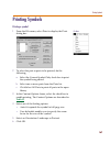
Printing symbols 167 printing symbols printing a symbol 1 from the file menu, select print to display the print dialog box. 2 to select the part or parts to be printed, do the following: a select the current symbol only check box to print the symbol being edited. B select one or more parts from the ...
Page 188
Chapter 5 using the symbol editor 168 table 13 content options option description symbol image specifies printing the graphics of the selected symbol attributes specifies printing the attributes and the attribute values of the selected symbol symbol data specifies printing the description, type, bbo...
Page 189: Overview
Creating and editing symbols 6 overview this chapter describes how to use the symbol editor to copy, create and edit symbols, which includes: creating new symbols on page 6-171 describes the four essential methods of creating a new symbol. Drawing symbol graphics on page 6-178 describes the assortme...
Page 190
Chapter 6 creating and editing symbols 170 configuring custom libraries on page 6-214 describes the procedure for making a custom library available in pspice schematics..
Page 191: Creating New Symbols
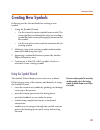
Creating new symbols 171 creating new symbols following are the four methods for creating a new symbol: 1 using the symbol wizard. • use the wizard to create symbols from scratch. The wizard guides you through the steps for creating a symbol and also creates packaging information for the symbol. • u...
Page 192
Chapter 6 creating and editing symbols 172 when you start the symbol wizard you are taken through a progression of screens, which provide you with information, ask you questions, and present you with choices, based on your selection in the first screen (shown below). Starting the symbol wizard 1 fro...
Page 193
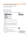
Creating new symbols 173 creating a symbol by copying another symbol an easy way to create a symbol is to make a copy of a similar symbol and modify the copy. Making a copy of a symbol copying a symbol from another library 1 from the part menu, select copy to display the copy part dialog box. 2 clic...
Page 194
Chapter 6 creating and editing symbols 174 importing a symbol definition import enables you to import a symbol that has been previously exported (see exporting a symbol on page 6-174 ) and incorporate it into a symbol library file. Importing a symbol 1 from the part menu, select import to display th...
Page 195
Creating new symbols 175 2 in the part name text box, enter the name of the symbol to be exported, or select it from the list. 3 in the file name text box, enter the name of the file to which the part definition is to be written. 4 click ok. Using ako symbols some of the orcad symbol libraries are m...
Page 196
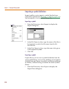
Chapter 6 creating and editing symbols 176 2 enter a name for the part in the part name text box (testcase, for example). 3 enter a description of the part in the description text box. 4 leave the ako name text box blank, and select do not display in the part browser check box. 5 click ok. Saving th...
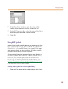
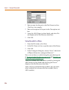
Page 197
Creating new symbols 177 creating an ako symbol 1 from the part menu in the symbol editor, select new. 2 in the part name text box, type a name for the part. 3 in the description text box, type a description of the part. 4 in the ako name text box, type the name of the base symbol (or example, ako t...
Page 198: Drawing Symbol Graphics
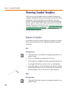
Chapter 6 creating and editing symbols 178 drawing symbol graphics there are several graphics tools available for drawing symbols. With these tools you can draw circles, lines, arcs, and boxes. You can also place pins and text on your symbol. The default properties of the individual display layers, ...
Page 199
Drawing symbol graphics 179 2 click at the location for the upper-left corner of the box. 3 move the pointer down and to the right. A dotted box outline follows the pointer. 4 click to set the lower-right corner of the box. Circle drawing a circle 1 click the draw circle button to change the pointer...
Page 200
Chapter 6 creating and editing symbols 180 adding arrowheads to polylines 1 select one or more polylines. 2 from the edit menu, select graphics properties. 3 select the appropriate arrowhead properties. 4 click ok. Pins adding pins to a symbol 1 click the place pins button to change the pointer to a...
Page 201
Drawing symbol graphics 181 an outline box follows the pointer that indicates the outline of the text string. 4 move the outline to the desired location and click to place the text. The outline box remains on the screen. You can click to place the same text string in several locations. 5 to stop pla...
Page 202
Chapter 6 creating and editing symbols 182 selecting selecting an element of a drawing 1 click to select the element. The object color (the default is set in the display preferences dialog box) indicates it is selected. 2 move or edit the object as necessary. Selecting a new object causes any previo...
Page 203
Drawing symbol graphics 183 filling shapes shapes that have been drawn using either the schematic editor or the symbol editor may be filled with color. In the symbol editor you can fill circles, rectangles, and polylines. Use the graphics properties dialog box to change properties on an instance bas...
Page 204
Chapter 6 creating and editing symbols 184 ordering drawing objects when you draw or paste an object in the symbol editor, pspice schematics places it in front of all other objects on the page or in a graphics frame. If the object is filled, it can obscure other objects. You can control how objects ...
Page 205
Drawing symbol graphics 185 rotating and flipping elements in the symbol editor, you can rotate and flip (mirror) elements currently being drawn, elements already drawn, and entire areas of a drawing. A rotated element is rotated 90° counter-clockwise. A flipped element is mirrored about the y-axis....
Page 206
Chapter 6 creating and editing symbols 186 flipping elements flipping an element before placing it on the drawing 1 press c+f to flip the element, while still in the drag mode. Flipping an already placed element 1 select the element. 2 press c+f to flip it. Flipping an area of the drawing 1 drag the...
Page 207
Drawing symbol graphics 187 moving moving an object 1 select an object (or group of objects). 2 place the pointer on the edge of the object or selected area and the annotation movement cursor becomes attached to the pointer. 3 drag and place the object at the desired location on the page. Resizing o...
Page 208: Editing Existing Symbols
Chapter 6 creating and editing symbols 188 editing existing symbols to edit an existing symbol, you must first load the library that the symbol is stored in. After the symbol is loaded, it can be edited by using all of the common editing functions that are available. To edit packaging information fo...
Page 209
Editing existing symbols 189 cutting, copying, and pasting the symbol editor has editing functions to cut, copy, paste, repeat, delete, and undelete selected objects. These functions are available under the edit menu, or can be accessed with keyboard shortcuts. The cut, copy, and delete functions ap...
Page 210
Chapter 6 creating and editing symbols 190 pasting paste places one or more copies of the last object stored in the buffer (from a cut or copy operation) onto the drawing. Pasting an object 1 from the edit menu, select paste to change the pointer to the shape of the object that was last cut or copie...
Page 211
Defining and editing pin types 191 defining and editing pin types pins establish the input and output terminals for symbols. For a pin you can: • select the type of graphic to display. • specify a pin name. • specify a pin number. • choose to display the name, the number, or both. Specifying pin typ...
Page 212
Chapter 6 creating and editing symbols 192 changing the type of a placed pin 1 select the pin and from the edit menu, select change. 2 in the type list box, select a pin type. 3 click ok. The change is only in effect for the selected pin. Changing the pin name as you placed pins, default names were ...
Page 213
Defining and editing pin types 193 displaying the pin name by default, pins you place on symbols will have their pin names displayed. To disable pin names, do the following: 1 double-click the pin or pin name to display the change pin dialog box. 2 select the display name check box to disable the na...
Page 214
Chapter 6 creating and editing symbols 194 defining and editing hidden power and ground pins with the symbol editor, you can set a pin to be invisible. If you set the visibility off, you must supply the name of a connecting net (typically a global net like $g_dpwr or $g_dgnd) for the pin in the net ...
Page 215
Defining and editing pin types 195 changing symbol origin and bounding box the origin is designated for placing a part, and is the point the part is rotated around. By default, the origin is at (0,0). It is maintained as a point of reference on the schematic. The bounding box defines the selection a...
Page 216
Chapter 6 creating and editing symbols 196 bounding box the bounding box is the rectangular dotted line surrounding the symbol. When you click a part from within the schematic editor, the area in which you can click and have that part be selected, is defined by the bounding box of the symbol. Resizi...
Page 217: Editing Symbol Attributes
Editing symbol attributes 197 editing symbol attributes you can add attributes (properties) to a symbol. When you add an attribute, you specify a name and a default value. This value can be changed when the symbol is used on a schematic. You can specify whether or not to display the attribute. There...
Page 218
Chapter 6 creating and editing symbols 198 2 in the name text box, type the name of the attribute. 3 optionally, type in the default value in the value text box. 4 by default, the attribute value only displays on the symbol. To disable any display, select none in the what to display frame. 5 by defa...
Page 219
Editing symbol attributes 199 editing a displayed attribute 1 double-click the displayed attribute. To edit an undisplayed attribute, or to make multiple changes, click the edit attributes button on the toolbar..
Page 220: Using Symbol Aliases
Chapter 6 creating and editing symbols 200 using symbol aliases a symbol has a name. It can also have one or more aliases associated with it. Aliases are alternative names that the device represented by the part are known by. For example, you can have a symbol named 74ac269 , which has as one of its...
Page 221: Specifying Part Packaging
Specifying part packaging information 201 specifying part packaging information if you are going to use a symbol for pcb layout, you will need to specify package or device information. Package information consists of: • the number of gates per package • a list of package types (footprints) where the...
Page 222
Chapter 6 creating and editing symbols 202 packaging definitions packaging information is kept in a package definition, separate from the symbol definition. Both are maintained using the symbol editor. By default, the name of the package definition for a symbol corresponds to the symbol name. This c...
Page 223
Specifying part packaging information 203 copying a package definition with the copy function in the packaging menu, you can create a new package definition from an existing one. It is the same as the copy function under the parts menu, the definition may be copied from the active library or a diffe...
Page 224
Chapter 6 creating and editing symbols 204 editing a package definition you can edit a package definition for the active symbol or for any package definition in the open package library. Editing the package definition for the active symbol 1 from the package menu, select edit to display the package ...
Page 225
Specifying part packaging information 205 2 click edit package types to display the edit package types dialog box. 3 in the package types per pin assignment text box, type the name of the package (for example, dip14) or select a type from the configured package types scroll list. 4 click add. 5 clic...
Page 226
Chapter 6 creating and editing symbols 206 specifying physical pin numbers for each package type (or group of package types that share the same pin-out) the physical pin numbers for each pin must be defined. The pin assignments frame in the package definition dialog box shows the pin numbers assigne...
Page 227
Specifying part packaging information 207 any changes you make to a pin assignment are not in effect until you select save assignment. If you make a change to a pin and then select another pin from the list without saving, the changes are not implemented. 7 when you are finished editing pins, click ...
Page 228
Chapter 6 creating and editing symbols 208 defining pin number assignments 1 from the packaging menu, select edit to display the package definition dialog box (see 6-205 ). 2 click edit pins to display the pin assignments dialog box (see 6-206 ). 3 in the pin no. Text box, type a pin number for each...
Page 229
Specifying part packaging information 209 specifying which pins can be swapped pins within a gate that are logically equivalent to one another can be swapped. Pin swapping is usually done during layout to minimize the complexities of circuit routing. Enabling pin swapping 1 from the packaging menu, ...
Page 230
Chapter 6 creating and editing symbols 210 creating components with multiple gate types some components consist of two or more different types of gates (for example, ecl devices). Each type of gate will have a different logical symbol with a unique name, but reference the same package definition. Fo...
Page 231
Specifying part packaging information 211 6 type a value in the value text box corresponding to one of the gate types specified in the package definition. Example: for the 10102nor symbol, gatetype = 1 (gates a,b,c); for the 10102ornor symbol, gatetype = 2 (gate d). 7 click save attr. 8 click ok to ...
Page 232
Chapter 6 creating and editing symbols 212 configuring package types when you create package definitions and specify package types for a device, you can pick from a list of commonly used package type names or enter one of your own. To add to the list of commonly used package type names that are pres...
Page 233
Specifying part packaging information 213 b type in the name of the new class in the package class text box. C click add. D click ok. 4 click add. 5 click ok..
Page 234: Configuring Custom Libraries
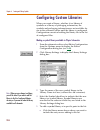
Chapter 6 creating and editing symbols 214 configuring custom libraries when you create a library, whether it is a library of symbols or a library of packaging information, the symbols and packaging information are not available for use in the schematic editor until the library is configured. Config...
Page 235
Configuring custom libraries 215 b type the name of the one you are adding in the library name text box. Be sure the appropriate check boxes are selected to indicate whether you are configuring just the symbol library, or the symbol and package library. 6 click add. 7 click ok. Note you may need to ...
Page 236: Example—Creating Symbols
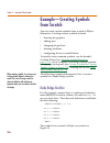
Chapter 6 creating and editing symbols 216 example—creating symbols from scratch you can create custom symbols from scratch in pspice schematics. Creating custom symbols includes: • drawing the graphics • adding pins • changing the grid size • defining attributes • configuring the new symbol library...
Page 237
Example—creating symbols from scratch 217 figure 19 example of diode bridge rectifier symbol opening or creating a symbol library to open or create a symbol library 1 in the schematic editor, from the file menu, select edit library to open the symbol editor. 2 to add this symbol to an existing symbo...
Page 238
Chapter 6 creating and editing symbols 218 • the type of the part—the part type is most commonly “component,” as it is in this example. • an ako or alias—use ako if you want it to inherit the graphics and attributes from another symbol. Use alias to assign additional names that this symbol can be us...
Page 239
Example—creating symbols from scratch 219 e draw a line at a 45-degree angle across the right angle of the symbol already created to denote the cathode. 4 place three copies of this diode: a drag the mouse to select the area that includes the graphics. Release the mouse to turn the lines red. If the...
Page 240
Chapter 6 creating and editing symbols 220 placing pins to place pins 1 from the graphics menu, select place pins. 2 to place the pins: a place the in+ and in- pins as shown in figure 19. B press c+ r to rotate the pin that is attached to the cursor. C place the out+ and out- pins as shown in figure...
Page 241
Example—creating symbols from scratch 221 3 from the graphics menu, select draw text to place the labels d1 through d4 on the diode symbols. 4 to change the size of the text, double-click the text and adjust the size. The number is a percentage relative to the usual size. 5 from the graphics menu, s...
Page 242
Chapter 6 creating and editing symbols 222 2 click part. A set its value to the name that you used in the original definition box. B click save attr. 3 click model. A set its value to the same value as in your model or subcircuit definition. B click save attr. 4 click template. The template attribut...
Page 243
Example—creating symbols from scratch 223 configuring the models the diode bridge symbol is now ready for use in pspice schematics, but the model library must also be configured if the design is going to be simulated. 1 from the analysis menu, select library and include files. 2 if the required libr...
Page 244
Chapter 6 creating and editing symbols 224.
Page 245: Creating And Editing
Creating and editing hierarchical designs 7 overview this chapter explains the procedures for creating and editing a hierarchical design. Many of the procedures used for creating and editing a hierarchical design are the same as those for creating and editing a design as explained in chapter 4, crea...
Page 246
Chapter 7 creating and editing hierarchical designs 226 setting up multiple views on page 7-237 describes how to set up and use alternate representations for a hierarchical block or symbol. Navigating through hierarchical designs on page 7-239 describes how to move between pages in a hierarchical de...
Page 247: Hierarchical Design Methods
Hierarchical design methods 227 hierarchical design methods you can create a hierarchical drawing in either of two ways: • create a block and later assign a schematic to the block (top-down method). • create a schematic and turn it into a symbol to be used in a higher level design (bottom-up method)...
Page 248: Blocks
Chapter 7 creating and editing hierarchical designs 228 creating and editing hierarchical blocks a hierarchical block represents a collection of circuitry in the form of one or more lower-level schematics. The block displays on a schematic as a rectangle with a variable number of input and output po...
Page 249
Creating and editing hierarchical blocks 229 changing the reference designator of the hierarchical block 1 double-click the hbn reference designator to display the edit reference designator dialog box. 2 type the reference designator in the package reference designator text box. 3 click ok to close ...
Page 250
Chapter 7 creating and editing hierarchical designs 230 3 type the new schematic name. 4 click ok. A new schematic displays and contains interface input and output ports corresponding to the pins connected to the block. The input ports correspond to the pins connected to the left side of the block. ...
Page 251
Creating and editing hierarchical blocks 231 editing a pin name on a hierarchical block 1 select the pin on the hierarchical block. 2 click the edit attributes button to display the change pin dialog box. 3 type the desired pin name in the pin name text box. 4 click ok. Deleting a pin on a hierarchi...
Page 252
Chapter 7 creating and editing hierarchical designs 232 associating an existing schematic instead of pushing into the block to create a schematic (see 7-229 ), you can associate an existing schematic with a hierarchical block. Associating an existing schematic with a hierarchical block 1 select the ...
Page 253: Symbols
Creating and editing hierarchical symbols 233 creating and editing hierarchical symbols pspice schematics uses two basic types of symbols: primitive and hierarchical. Primitive symbols are low level symbols that explicitly contain all of the information required by the netlister. They can be modifie...
Page 254
Chapter 7 creating and editing hierarchical designs 234 connected to, is created for each hidden pin. Hidden pins are especially useful for global power and ground on digital parts ($g_dpwr, $g_dgnd). Symbolizing a schematic 1 open the schematic. 2 from the file menu, select symbolize to display the...
Page 255
Creating and editing hierarchical symbols 235 converting hierarchical blocks to symbols when you finish editing a hierarchical block, you have the option of turning the block into a symbol. By making the block a symbol, you make it available for use in other schematics. Converting a block to a symbo...
Page 256: Using Interface Ports
Chapter 7 creating and editing hierarchical designs 236 using interface ports when you use a block or symbol to represent an underlying schematic, connections to the underlying schematic are made by means of the pins on the block or symbol. The pins on the block or symbol must correspond to interfac...
Page 257: Setting Up Multiple Views
Setting up multiple views 237 setting up multiple views a view is an underlying representation of a hierarchical block or symbol. A block can have more than one underlying representation by having multiple views. For example, you can define a part that has a transistor-level schematic as one view an...
Page 258
Chapter 7 creating and editing hierarchical designs 238 setting up an associated view for the translator 1 from the options menu, select translators to display the translators dialog box. 2 select a translator from the list or type a name in the translator text box. 3 type the name of the view in th...
Page 259: Designs
Navigating through hierarchical designs 239 navigating through hierarchical designs the navigate menu has functions that enable you to move between pages, create new pages, delete pages, and copy pages. You can move within a hierarchical design using functions from the navigate menu. You can push in...
Page 260
Chapter 7 creating and editing hierarchical designs 240 finding where active schematic fits in a hierarchy 1 from the navigate menu, select where to display the where dialog box. The dialog box shows where the open schematic fits in the hierarchy of the open design. 2 click ok. Navigate menu.
Page 261: Values
Assigning instance-specific part values 241 assigning instance-specific part values the edit schematic instance function enables you to view and edit the instance specific attributes associated with the instance of the block or hierarchical symbol that you pushed into. You can only add, change, or d...
Page 262: Passing Information Between
Chapter 7 creating and editing hierarchical designs 242 passing information between levels of hierarchy with pspice schematics, you can create a lower-level schematic such that different instances of it will have different component values. For instance, a lower-level schematic contains a certain re...
Page 263
Passing information between levels of hierarchy 243 found at that level, pspice schematics then searches the parent level. It continues up the hierarchy until it either finds a definition or until it reaches the top of the hierarchy. • when pspice schematics finds an attribute, it evaluates the attr...
Page 264: Example—Creating A
Chapter 7 creating and editing hierarchical designs 244 example—creating a hierarchical design this example shows you how to create schematics from the top level down. The design consists of a simple schematic with a block representing a cmos inverter and a lower-level schematic for the inverter. Fo...
Page 265
Example—creating a hierarchical design 245 placing the voltage source 1 click the get new part button to display the part browser dialog box. 2 enter vsrc in the part field. 3 click place & close. 4 move the part symbol to the desired location and click to place the symbol. 5 right-click to stop pla...
Page 266
Chapter 7 creating and editing hierarchical designs 246 6 enter cmosinv in the text box. This changes the value of the refdes attribute from hb1 to cmosinv. 7 click ok. Drawing the output load resistor 1 click the get new part button to display the part browser dialog box (see 7-245 ). 2 type r in t...
Page 267
Example—creating a hierarchical design 247 wiring the symbols now that you have placed all of the symbols, wire the symbols to look like the schematic shown in figure 20. 1 click the draw wire button to change the pointer to a pencil. 2 click the top of v1. Click at the location of the wire vertex (...
Page 268
Chapter 7 creating and editing hierarchical designs 248 saving your work as a top-level schematic 1 click the save file button. 2 type tlcmos as the name of the file (the .Sch extension is assigned by default). 3 click ok. Drawing the lower-level schematic the top-level design is complete. Now you c...
Page 269
Example—creating a hierarchical design 249 selecting the block and naming the new schematic 1 click the cmosinv block to select it. 2 from the navigate menu, select push. Because the block is new, the setup block dialog box appears. 3 enter the new schematic name, cmos . 4 click ok. 5 move the inter...
Page 270
Chapter 7 creating and editing hierarchical designs 250 6 right-click to stop placing parts. 7 click the get new part button to display the part browser dialog box (see 7-245 ). 8 enter m2n6802 in the part text box. 9 click place & close. 10 move the part symbol to the desired location of m2 and cli...
Page 271
Example—creating a hierarchical design 251 drawing the wires click the draw wire button and draw wires to connect parts and symbols as shown in figure 21. Saving the file click the save file button to save the schematic. You are not prompted for a file name because the schematic was named when you p...
Page 272
Chapter 7 creating and editing hierarchical designs 252.
Page 273: Preparing Your Design For
Preparing your design for simulation 8 overview this chapter provides guidelines for preparing your schematic for simulation and references further information contained in your pspice user’s guide. A design that is targeted for simulation will have: • parts that there are simulation models availabl...
Page 274
Chapter 8 preparing your design for simulation 254 editing simulation models from pspice schematics on page 8-258 . Adding and defining stimulus on page 8-259 . Starting the simulator on page 8-266 . Viewing results on page 8-267 ..
Page 275: And Board Layout
Creating designs for simulation and board layout 255 creating designs for simulation and board layout when creating designs for both simulation and printed circuit board layout, some of the parts you use will be for simulation only (for example, simulation stimulus parts like voltage sources), and s...
Page 276
Chapter 8 preparing your design for simulation 256 handling unmodeled pins parts that have some pins that are not modeled, will appear broken when placed on the schematic. To see an example of this, place an instance of the pm-741 part from the “opamp.Slb” symbol library. The os1 and os2 pins are no...
Page 277: Specifying Simulation Model
Specifying simulation model libraries 257 specifying simulation model libraries refer to the creating models chapter of your pspice user’s guide for information about creating and configuring simulation model libraries. Each part that you intend to simulate must have a simulation model defined. Chec...
Page 278: Pspice Schematics
Chapter 8 preparing your design for simulation 258 editing simulation models from pspice schematics you can define and edit simulation models directly from pspice schematics. Models can be defined using the parts utility or the text editor (sometimes called the model editor). The parts utility is us...
Page 279: Adding and Defining Stimulus
Adding and defining stimulus 259 adding and defining stimulus the stimulus editor is a utility that enables you to set up and verify the input waveforms for a transient analysis. You can create and edit voltage sources, current sources, and digital stimuli for your circuit. Menu prompts guide you to...
Page 280
Chapter 8 preparing your design for simulation 260 setting up analyses refer to your pspice user’s guide for information about setting up and running the many different analysis types supported by pspice a/d. Creating a simulation netlist overview a netlist is the connectivity description of a circu...
Page 281
Adding and defining stimulus 261 note for release 9.2, the maximum limits have been removed for the following .Subckt arguments: nodes, parameters, and optional nodes. Hierarchical netlists are especially useful to ic designers who want to perform layout vs. Schematic (lvs) verification because they...
Page 282
Chapter 8 preparing your design for simulation 262 for release 9.2, markers can now be placed on subcircuit nodes as well. This allows you to perform cross-probing between schematics and pspice at the lower level circuits of a hierarchical design. Note if conditional constructs are used, the hierarc...
Page 283
Adding and defining stimulus 263 3 if you want the .Param commands to be made global in scope, check the make .Param commands global checkbox. If this is disabled, the param symbols will be local to the subcircuit in which they occur. 4 click ok. Note to save the current settings and make them becom...
Page 284
Chapter 8 preparing your design for simulation 264 note the lvs netlist is written in general syntax and should be compatible with most lvs tools. Depending on the tool you intend to use, however, you may need to modify the file in particular ways in order for it to be usable with your specific syst...
Page 285
Adding and defining stimulus 265 use the control buttons located directly above the use template list box to configure the list of templates. You can: • add a new template by clicking the new icon or by double-clicking in the dashed box at the beginning of the list. • delete a template by selecting ...
Page 286: Starting The Simulator
Chapter 8 preparing your design for simulation 266 4 with the subparam part still selected, from the edit menu, choose attributes. 5 in the attributes dialog box, define the names and default values for the attributes that can be changed on an instance-by-instance basis. 6 in the top-level schematic...
Page 287: Viewing Results
Viewing results 267 viewing results you can use probe to view and perform waveform analysis of the simulation results. For more information, refer to the waveform analysis chapter of yourpspice user’s guide. Viewing bias point results after simulating, you can display bias point information on your ...
Page 288
Chapter 8 preparing your design for simulation 268 using markers you can place markers on your schematic to indicate the points in probe where you want to see waveforms displayed. Note for release 9.2, markers can now be placed on subcircuit nodes as well. This allows you to perform cross-probing be...
Page 289
Viewing results 269 configuring probe display of simulation results to configure what probe displays when it is started, select probe setup from the analysis menu. You are given the following choices: • restore last probe session—this restores the display characteristics from the last session of pro...
Page 290
Chapter 8 preparing your design for simulation 270
Page 291: Using Design Journal
Using design journal 9 overview this chapter provides introductory information about the design journal. In this chapter you will find the following sections: understanding design journal on page 9-272 describes the purpose and different uses of design journal. Design journal help on page 9-273 desc...
Page 292: Understanding Design Journal
Chapter 9 using design journal 272 understanding design journal design journal is a very powerful analysis and tracking tool. With it you can: • document stages of development • perform what-if analysis on your current schematic, while preserving the integrity of the original • compare the results o...
Page 293: Design Journal Help
Design journal help 273 figure 22 a working schematic and two checkpoint schematics when documenting development stages and performing what-if analysis, you can: • perform all pspice schematics, pspice, and probe operations on a checkpoint schematic • create up to 999 checkpoint schematics • restore...
Page 294
Chapter 9 using design journal 274.
Page 295: Preparing Your Design For
Preparing your design for board layout 10 overview this chapter describes how to prepare your design for use with a board layout program and has the following sections: connectors on page 10-277 describes placing connectors to provide the interface between the pcb and the rest of the system. This se...
Page 296
Chapter 10 preparing your design for board layout 276 interfacing to board layout products on page 10-292 describes the procedures for using pspice schematics with the board layout products from other vendors..
Page 297: Connectors
Connectors 277 connectors connectors provide the interface between a pcb and the rest of a system. The distinction between connectors and ports on a schematic is important and is shown in table 14. Off-page ports are not physical connectors, so you cannot use an off-page port as a connector or a con...
Page 298
Chapter 10 preparing your design for board layout 278 using connector symbols that represent the entire connector these symbols will have as many pins as the physical connector they represent. You can wire signals directly to the pins or connect labeled off-page (or global) ports to each pin. The la...
Page 299
Connectors 279 creating single-pin connector symbols when creating a connector pin symbol, you must correctly define the connector package for the layout netlist to be correct. For example, in creating a 62-pin edge connector, instead of creating a single symbol for a 62-pin edge connector with all ...
Page 300: Packaging The Parts In Your
Chapter 10 preparing your design for board layout 280 packaging the parts in your design symbols used in pspice schematics represent either an individual gate of a packaged device, or a complete device. When a symbol representing a single gate is placed on a schematic, it is assigned a unique refere...
Page 301
Packaging the parts in your design 281 pin numbers for devices with package definitions are determined from the package definition rather than from the symbol. • pin numbers are dependent on the gate (for multi-gate parts) and package type (for devices with alternative pin assignments based on packa...
Page 302
Chapter 10 preparing your design for board layout 282 2 type a new value in the package reference designator text box. 3 click ok. If you have other parts that you want to automatically package together, use the all except user-assigned option when you package the design. Automatically packaging at ...
Page 303
Packaging the parts in your design 283 assigning reference designators automatically use the package selection from the tools menu to package individual parts into physical packages. Packaging and assigning reference designators 1 from the tools menu, select package to display the package dialog box...
Page 304
Chapter 10 preparing your design for board layout 284 setting package class priorities priorities can be set (for the packager) to use in determining which package type to assign when a part is available in more than one type. For example, you could specify that a dip package type be used. If the pa...
Page 305
Packaging the parts in your design 285 5 if you want to insert a class into the class priorities list, first select a class from the package classes list, then select an item in the class priorities list and click insert. The package class is added to the list before the item selected in the class p...
Page 306: Report
Chapter 10 preparing your design for board layout 286 generating a bill of materials report a bill of materials report lists the quantities of each component type used in the design along with corresponding reference designators. You can also include information such as values for part instance attr...
Page 307
Generating a bill of materials report 287 generating a bill of materials report 1 select reports from the file menu to display the reports dialog box. 2 click display. The bill of materials dialog box appears and you can print, display, or save the report. Closing the reports dialog box 1 click clos...
Page 308
Chapter 10 preparing your design for board layout 288 customizing the format of the report 1 click setup to display the report setup dialog box. 2 in the format text box, type the attributes to be displayed in the report according to the following syntax: [descriptive text]@attribute name> where the...
Page 309
Generating a bill of materials report 289 user defined component information you can display user-specific component information (such as, costs and in-house part numbers) in the bill of materials report. The bill of materials report will take a component description file as input. The component des...
Page 310
Chapter 10 preparing your design for board layout 290 the cost entries for 10k and 1k resistors would appear in the component description file as follows: r,rc05,r1,value,10k r,rc05,r1,cost,.05 r,rc05,r2,value,1k r,rc05,r2,cost,.03 specifying user-defined component attribute descriptions 1 from the ...
Page 311: Swapping Pins
Swapping pins 291 swapping pins to swap pins on a given gate, add a swap attribute with the value of the pin names of the two pins to be swapped. For example: swap=a b will swap pin a with pin b. Swapping pins 1 from the edit menu, select attributes to display the attribute editing dialog box. 2 in ...
Page 312: Interfacing to Board Layout
Chapter 10 preparing your design for board layout 292 interfacing to board layout products pspice schematics creates layout netlists in the formats shown in table 15. Selecting a layout format 1 from the tools menu, select configure layout editor to display the configure tools dialog box. 2 from the...
Page 313
Interfacing to board layout products 293 creating a layout netlist 1 from the tools menu, select create layout netlist. Note if you are using the orcad line of products, you will be preparing the netlist as input to orcad layout. Although schematics does not generate a netlist file (.Mnl) that is di...
Page 314
Chapter 10 preparing your design for board layout 294 layout mapping files when creating layout netlists, pspice schematics uses mapping files. These files let you customize the handling by the layout netlister of part, net, and package type names. Mapping files are text files that you can edit with...
Page 315
Interfacing to board layout products 295 common syntax each file ( .Xmp , .Xnt and .Xpk ) consists of a number of lines. Empty lines and those starting with the ‘#’ character are ignored. Otherwise, a line consists of one or more comma-separated identifiers followed by either an ako specification or...
Page 316
Chapter 10 preparing your design for board layout 296 parts list mapping (.Xmp) after pspice schematics has found a matching rule in the map file for the component or part attribute of a part, it further processes the replacement string. This processing is similar to the processing of the template a...
Page 317
Interfacing to board layout products 297 c101 cap,10uf or c102 cap,10uf,20% depending on whether or not a tolerance attribute has been specified. The value attribute must be defined; pspice schematics will issue a message if a capacitor has no assigned value. To support the case where the designer w...
Page 318
Chapter 10 preparing your design for board layout 298 the following rules in the .Xpk file will implement this: dip* cc* -cc note that the dip* rule is empty; it matches package classes such as dip14, but there is no resulting replacement string. The lcc* rule matches all strings that start with lcc...
Page 319
Interfacing to board layout products 299 using back annotation 1 from the tools menu, select back annotate to display the back annotate dialog box. 2 type the name of the eco file generated by the layout package in the eco file name text box. 3 select an eco file format from the eco file format list...
Page 320
Chapter 10 preparing your design for board layout 300
Page 321: Exporting Dxf Files
Exporting dxf files a overview this appendix provides information regarding exporting dxf files. In this chapter you will find the following sections: exporting dxf files on page a-302 . Exporting from the schematic editor on page a-303 . Exporting in the symbol editor on page a-304 ..
Page 322: Exporting Dxf Files
Chapter a exporting dxf files 302 exporting dxf files the export function generates drawing interchange format (dxf) files. These files are also known as autocad format 2-d files. You can export the entire schematic drawing, a page, a portion of a page, or symbol graphics to a dxf file..
Page 323: Exporting From The Schematic
Exporting from the schematic editor 303 exporting from the schematic editor 1 from the file menu, select export to display the export dialog box. 2 select one of the following options: • click select all to export all pages of the schematic file. • select one of the entries in the pages dialog box t...
Page 324
Chapter a exporting dxf files 304 exporting in the symbol editor 1 from the file menu, select export to display the export dialog box. 2 select one of the following options: • click select all to export all symbols in the current symbol library. • select any of the entries in the symbols dialog box ...
Page 325: Library Expansion and
Library expansion and compression utility b overview this appendix explains the library and expansion compression utility that can be used with the pspice schematics libraries. In this chapter you will find the following sections: using the library utility on page b-306 . Expanding library definitio...
Page 326: Using The Library Utility
Chapter b library expansion and compression utility 306 using the library utility pspice schematics includes a library utility (lxcwin) that works with the symbol, package, and footprint libraries. You can use lxcwin to: • expand a library into definitions and create a list of those definitions (. L...
Page 327: Into Text Files
Expanding library definitions into text files 307 expanding library definitions into text files when you use lxcwin to expand a library, it reads the selected library line by line, and writes each definition of a symbol (.Sym), package (.Pkg), or footprint (.Fpd) in plain ascii format, to a text fil...
Page 328: Salvaging A Corrupted File
Chapter b library expansion and compression utility 308 salvaging a corrupted file to salvage a corrupted file or one that has carriage returns and line feeds 1 in the action frame, select fix index. 2 click the process file button. 3 select a library. Reorganizing a library file to reorganize a lib...
Page 329: Running Lxcwin Using
Running lxcwin using command line options 309 running lxcwin using command line options you can also run lxcwin using command line options. The options are: example: lxcwin *.Flb -f fix index (default) -x expand -c compress -n do not delete definition files one or more library names; the names may i...
Page 330
Chapter b library expansion and compression utility 310
Page 331: Advanced Netlisting
Advanced netlisting configuration items c overview this appendix contains information regarding advanced netlisting configuration. In this chapter you will find the following sections: specifying pspice node name netlisting preferences on page c-312 . Specifying board layout node name netlisting pre...
Page 332: Specifying Pspice Node Name
Chapter c advanced netlisting configuration items 312 specifying pspice node name netlisting preferences by default, the pspice netlister assigns names such as $n_001 to nodes that are not explicitly labeled. You can change the format that the netlister uses to create these names by using a text edi...
Page 333: Specifying Board Layout Node
Specifying board layout node name netlisting preferences 313 specifying board layout node name netlisting preferences to change any of these settings, use a text editor and edit the pspice.Ini file in the windows directory. Pcbhierpathsep is the separator character to use when creating hierarchal ne...
Page 334: Customizing Edif Netlists
Chapter c advanced netlisting configuration items 314 customizing edif netlists you can change the amount each level in the netlist is indented by changing the edifindent item in the [schematics] section of the pspice.Ini initialization file. Use a text editor to edit the pspice.Ini file in the wind...
Page 335: Attribute List
Attribute list d overview this appendix is a list of attribute names used by pspice schematics and descriptions of each of those attributes. When you use the symbol editor to create a new symbol, the part , model , refdes, and template attributes are.
Page 336
Chapter d attribute list 316 provided as a default set. You can provide any other attributes as needed. Table 1 reserved attributes attribute description see notes component the name of the package definition to be used for a part. If the name of the package definition is the same as the part name, ...
Page 337
Overview 317 model the name of the model referenced for simulation. This name must match the name of the .Model or .Subckt definition of the simulation model as it appears in the model library file (.Lib). For example, if your design includes a 2n2222 bipolar transistor, with the .Model name q2n2222...
Page 338
Chapter d attribute list 318 pkgtype the physical carrier type to be used for the part. (examples: dip14, lcc20, dip8). If the package definition for the part has only one available package type defined, then the pkgtype attribute will be assigned this value. You can manually assign the package type...
Page 339
Overview 319 template the recipe for creating a netlist entry for simulation. The pin names specified in the template must match the pin names on the symbol. The number and order of the pins listed in the template must match those appropriate for the associated .Model or .Subckt definition reference...
Page 340
Chapter d attribute list 320
Page 341: Symbol Libraries
Symbol libraries e overview this appendix contains the contents of the symbol libraries that are provided with pspice schematics..
Page 342: Using Symbol Libraries
Chapter e symbol libraries 322 using symbol libraries symbols are stored in symbol libraries. The symbol library files have a .Slb extension and contain graphical representations and attributes of parts. The contents of the symbol libraries provided with pspice schematics are listed in table 2. Part...
Page 343
Using symbol libraries 323 table 2 symbol libraries symbol library file name contents 7400.Slb 7400-series ttl 74ac.Slb advanced cmos 74act.Slb ttl-compatible, advanced cmos 74als.Slb advanced low-power schottky ttl 74as.Slb advanced schottky ttl 74f.Slb fast 74h.Slb high-speed ttl 74hc.Slb high-spe...
Page 344
Chapter e symbol libraries 324 anlg_dev.Slb analog devices inc.: operational amplifiers, transistor arrays, buffers, voltage references, analog multipliers, analog switches apex.Slb apex microtechnology corporation: operational amplifiers atmel.Slb † atmel corporation: eeprom, prom, sram, pld bipola...
Page 345
Using symbol libraries 325 dig_pal.Slb programmable array logic devices dig_prim.Slb digital primitives for use with plsyn as well as general simulation purposes diode.Slb diodes, zener diodes, current regulator diodes, varactors ebipolar.Slb european bipolar transistors ecl.Slb † motorola corp., na...
Page 346
Chapter e symbol libraries 326 hyundai.Slb † hyundai electronic inc. Ltd.: pld, dram, sram intel.Slb † intel corp.: eprom, cpu, math co-processors, microcontrollers, sram, network processors jbipolar.Slb japanese bipolar transistors jdiode.Slb japanese diodes, rectifiers, zener diodes, varactors, sc...
Page 347
Using symbol libraries 327 misc.Slb timers, cmos transistor arrays, variable admittance, variable impedance, three-phase transformers, relays, dc motor, time-dependent switches mitmem.Slb † mitsubishi electric corporation: eeprom, prom, dram, sram mitram.Slb † mitsubishi electric corporation: dram, ...
Page 348
Chapter e symbol libraries 328 nsucont.Slb † national semiconductor inc.: microcontrollers oki.Slb † oki semiconductor: display drivers, dram, eeprom, eprom, dram, sram, microcontrollers, clock, speech synthesis, recorders, codec, modems opamp.Slb operational amplifiers, voltage comparators, voltage...
Page 349
Using symbol libraries 329 swit_rav.Slb averaged switched-mode power supply blocks swit_reg.Slb switched-mode regulators tex_inst.Slb texas instruments inc.: operational amplifier, voltage comparators thyristr.Slb scr, triac, ujt ti1.Slb † texas instruments inc.: line drivers, transceivers, display ...
Page 350
Chapter e symbol libraries 330 xicor.Slb † xicor inc.: sram, eeprom, potentiometers xtal.Slb quartz crystals zilog.Slb † zilog inc.: i/o controllers, cpu, counters table 2 symbol libraries (continued) symbol library file name contents.
Page 351: Glossary
Glossary abm analog behavioral model. A view of a hierarchical schematic used for analysis. See also view. Ako “a kind of” symbol. Symbols must either contain graphics or refer to an ako symbol. The ako defines the symbol in terms of the graphics and pins of another part. Both must exist in the same...
Page 352
Glossary may 16, 2000 332 bounding box a rectangular dotted line containing the graphics for a symbol and all visible pin connection points. In terms of the schematic editor, the position of the bounding box determines whether a point falls on a part when selecting parts, or whether it falls on the ...
Page 353
***draft*** glossary 333 global port provides a connection to another global port of the same name anywhere in the schematic. Gravity the property of a drawing object to snap to the nearest grid or pin when being placed on a drawing or moved about a drawing. Gravity radius the distance between the c...
Page 354
Glossary may 16, 2000 334 navigation the process of moving between pages in a multi-sheet schematic, or between levels in a hierarchical design. Net a set of electrically connected part pins. A net may be anonymous or named. An anonymous net might be the junction of two resistors. A named net could ...
Page 355
***draft*** glossary 335 part outline consists of the symbol for a part (graphics and pins), minus any text. Pin contained in parts, ports and off-page connectors. Parts can contain multiple pins. Each part contains specific pin names associated with the part. Pins may connect to a wire, a bus or an...
Page 356
Glossary may 16, 2000 336 selection area when drawing or editing a schematic or symbol, the area identified and enclosed by a region-of-interest (roi) box for the purpose of performing some operation on the objects within the area. Setpoint a special symbol used to specify initial node voltages duri...
Page 357: Index
Index a a kind of, see ako abm , 331 accessing symbols , 188 add text dialog box , 127 adding annotation graphics , 130 annotation text , 126 attributes , 90 library , 44 multiple line text , 126 non-electrical information , 126 package type , 212 package type for a component , 204 page to design , ...
Page 358
Index 338 arc, drawing , 178 archive , 24 assigning annotation , 89 attribute names , 315 attribute value , 93 instance-specific part values , 241 pin numbers , 208 pins , 201, 206 reference designator , 14, 97, 228, 281 attribute definition of , 331 deleting , 90 editing , 88 enabling display , 91 ...
Page 359
Index 339 c cadstar layout format , 292 change attribute dialog box , 91, 158 change pin dialog box , 160, 192, 231, 247 change text dialog box , 161, 181 changing a placed pin type , 192 application settings , 64 attribute text , 158 attribute value , 93 border style , 52 bounding box size , 196 cu...
Page 360
Index 340 copying between pages , 138 package definition , 203 page , 137 part , 94 selected object , 189 symbol , 173 to clipboard , 121 create page dialog box , 136 creating ako symbol , 177 annotation items , 126 annotation symbols , 134 base symbol , 175 connections between pages , 137 connector...
Page 361
Index 341 back annotate , 299 block view , 232 change attribute , 91, 158 change pin , 160, 192, 231, 247 change text , 161, 181 configure tools , 292 configuring package types , 212 copy package definition , 203 copy page , 137 copy part , 94, 173 create page , 136 definition , 200 delete page , 13...
Page 362
Index 342 drawing additional pages , 136 arc , 178 area , 54 block , 35 box , 178 bus , 12, 35, 106–107 circle , 179 connections , 107 custom power and ground symbols , 103 line , 179 lower-level schematic , 248 options , 109 orthogonal wires and buses , 109 symbol graphics , 178 text , 38, 127, 180...
Page 363
Index 343 associating with a hierarchical block , 232 export file specification dialog box , 303 export parts dialog box , 174 exporting bill-of-materials report , 290 dxf files , 301 from the schematics editor , 303 in the symbol editor , 304 symbol , 174 f file management , 19 opening , 33 saving ...
Page 364
Index 344 navigating through , 239 passing information between levels , 242 hierarchical parts , 29 hierarchical symbol , 233 selecting , 239 horizontal offset , 96 hotspot definition of , 333 i import dialog box , 174 import orcad file dialog box , 303 importing annotation graphics , 133 bitmaps , ...
Page 365
Index 345 message definition of , 333 message viewer , 74 additional information , 76 closing , 76 severity indicator , 74 using , 73 metafiles importing , 133, 181 mirroring, see flipping model behavioral , 237 definition , 80 library , 80 name , 316 simulation , 256, 322 model definition definitio...
Page 366
Index 346 orthogonality , 109 printing , 140 scaling , 141 specifying gravity , 164 text grid , 165 origin , 195 definition of , 334 orthogonal connectivity , 109 drawing wires and buses , 109 enabling , 110 with rubberbanding enabled , 112 outline border style , 53 p package definition of , 334 inf...
Page 367
Index 347 definition of , 334 part instance changing display of attributes , 91 definition of , 334 part origin editing , 195 part outline definition of , 335 part value, changing , 14 parts placing and editing , 85 stopping placement , 85 passing information between levels of hierarchy , 242 pastin...
Page 368
Index 348 properties changing , 128 protel layout format , 292 pushing , 239 into block , 227 r redraw button , 34, 39, 153, 155 reference designator assigning , 97, 281 auto-naming , 97 changing , 14, 229 definition of , 335 value , 318 refreshing the screen , 39 remove package definition dialog bo...
Page 369
Index 349 library , 84 multiple elements , 182 multiple objects , 116 objects on schematic , 116 part by description , 83 part by name , 81 part for editing , 188 part from symbol library , 84 parts , 8 selection area definition of , 336 selection rectangle , 116 set attribute level dialog box , 242...
Page 370
Index 350 editing , 2, 94, 188 elements of , 178 exporting , 174 global port , 102 hierarchical , 233 library , 42, 80, 173, 321 placing , 85 port , 30 primitive , 233 printing , 167 stopping placement , 85 wiring , 247 symbol aliases , 200 symbol attribute component , 316 gate , 316 gatetype , 316 ...
Page 371
Index 351 enable bias voltage display , 37 get new part , 82, 155 insert picture , 38, 133, 181 marker color , 36 more info , 76 new file , 33, 79, 154 new symbol , 155, 172 open file , 33, 79, 154 place pins , 155, 180 print , 33, 140 redraw , 34, 39, 153, 155 save file , 33, 154, 248 select part ,...
Page 372
Index 352 moving , 15 orthogonal , 109 rewiring segment , 105 selecting , 116 wire segment adding , 104 wiring symbols , 247 wizard symbol creation , 171 workspaces , 19 z zoned border style , 53 zoom area button , 34, 68, 154 zoom factor , 142 zoom in button , 34, 68, 154 zoom out button , 34, 69, ...

