- DL manuals
- Caen
- Measuring Instruments
- N6724
- User Manual
Caen N6724 User Manual
Summary of N6724
Page 1
User manual um3247 n6724 2/4 channel 14bit 100 ms/s waveform digitizer rev. 10 - january 27 th , 2017.
Page 2: Purpose Of This Manual
Purpose of this manual this document contains the full hardware descrip on of the n6724 caen digi zer and their principle of opera ng as waveform recording digi zer (basing on the herea er called ”waveform recording firmware”). The reference firmware revision is: 4.12_0.14. For any reference to regist...
Page 3
Caen s.Pa. Via vetraia, 11 55049 viareggio (lu) - italy tel. +39.0584.388.398 fax +39.0584.388.959 info@caen.It www.Caen.It ©caen spa – 2017 disclaimer no part of this manual may be reproduced in any form or by any means, electronic, mechanical, recording, or otherwise, without the prior wri en perm...
Page 4: Index
Index purpose of this manual . . . . . . . . . . . . . . . . . . . . . . . . . . . . . . . . . . . . . . . . . . . . . . . 2 change document record . . . . . . . . . . . . . . . . . . . . . . . . . . . . . . . . . . . . . . . . . . . . . . 2 symbols, abbreviated terms and nota on . . . . . . . . . ....
Page 5: List Of Figures
Test pa ern generator . . . . . . . . . . . . . . . . . . . . . . . . . . . . . . . . . . . . . . . . . . . 45 reset, clear and default configura on . . . . . . . . . . . . . . . . . . . . . . . . . . . . . . . . . . 45 global reset . . . . . . . . . . . . . . . . . . . . . . . . . . . . . . . . . . ...
Page 6: List Of Tables
Fig. 7.9 example of non-overlapping n lbk and n lfwd in case of posi ve logic (le ) and nega ve logic (right). 36 fig. 7.10 event format for non-overlapping n lbk and n lfwd .In case of posi ve logic (le ) and nega ve logic (right). . . . . . . . . . . . . . . . . . . . . . . . . . . . . . . . . . ....
Page 7: Safety No Ces
Safety no ces caution: this product needs proper cooling. Use only crates with forced cooling air flow since overheating the board may degrade its performances! Caution: this product needs proper handling. N6724 does not support live insertion (hot swap)! Remove or insert the board when the nim crat...
Page 8: 1 Introduc On
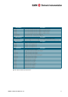
1 introduc on the mod. N6724 is a 1-unit wide nim module housing a 2/4 channel 14 bit 100 ms/s desktop waveform digi zer with 2.25 v pp input dynamic range on single ended mcx coaxial connectors. Customized versions of 10 v pp and 500 mv pp input range are available (see tab. 1.1). The dc offset is a...
Page 9
Board model descrip on n6724b 4 ch. 14 bit 100 ms/s waveform digi zer: 512 ks/ch, c20, se n6724c 2 ch. 14 bit 100 ms/s waveform digi zer: 512 ks/ch, c20, se n6724f 4 ch. 14 bit 100 ms/s waveform digi zer: 4 ms/ch, c20, se n6724g 2 ch. 14 bit 100 ms/s waveform digi zer: 4 ms/ch, c20, se pers0172401 7...
Page 10: 2 Block Diagram
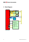
2 block diagram dac amc [fpga] adc & memory controller adc buffers x4 (4 channels) roc [fpga] - readout control - optical link control - usb interface control - trigger control - external interface control mux osc clock manager (ad9520) local bu s clk in trg in gpi usb inputs front panel gpo optical...
Page 11
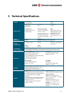
3 technical specifica ons general form factor: 1-unit wide nim weight 870 g analog input channels 2/4 channels single ended connector mcx bandwidth 40 mhz impedance (z in ) 50 Ω @2.25v pp / 0.5v pp 1000 Ω @10v pp full scale range (fsr) 2.25 v pp or customizable to 0.5 v pp / 10 v pp abs max ra ng ( @...
Page 12
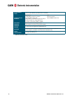
Adc & memory contr. Altera cyclone ep1c20 (one fpga serves 1 channel) communication interface op cal link caen conet proprietary protocol up to 80 mb/s transfer rate daisy-chain: it is possible to connect up to 8 or 32 adc modules to a single op cal link controller (respec vely a2818 or a3818) usb u...
Page 13
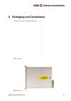
4 packaging and compliancy the module is housed in a single-width nim unit. Fig. 4.1: front view fig. 4.2: side view um3247 - n6724 user manual rev. 10 13.
Page 14
Caution: to manage the product, consult the opera ng instruc ons provided. A potential risk exists if the operating instructions are not followed! Caution: this product needs proper cooling. Use only crates with forced cooling air flow since overheating the board may degrade its performances! Cautio...
Page 15: 5 Power Requirements
5 power requirements the table below resumes the n6724 power consump ons per relevant power supply rail. Module supply voltage +6 v -6 v n6724 3.9 a 90 ma tab. 5.1: power requirements table um3247 - n6724 user manual rev. 10 15.
Page 16: 6 Panels Descrip On
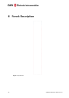
6 panels descrip on fig. 6.1: front panel view 16 um3247 - n6724 user manual rev. 10
Page 17: Front Panel
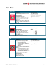
Front panel analog input function input connectors from ch0 to ch3 receive the input analog signals. Electrical specs input dynamics: 2.25 v pp input impedance (z in ): 50 Ω. Absolute max analog input voltage: 6 v pp (with v rail max +6 v or –6 v) for any dac offset value. Note: 0.5 (50 Ω) and 10 v p...
Page 18
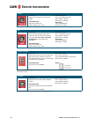
Trg-in function digital input connector for the external trigger. Electrical specs signal level: nim or ttl. Input impedance (z in ): 50 Ω. Mechanical specs series: 101 a 004 connectors. Type: dlp 101 a 004-28. Manufacturer: fischer. Alterna vely: type: epl 00 250 ntn. Manufacturer: lemo. Gpi functi...
Page 19
Diagnostics leds dtack (green): indicates there is a read/write access to the board; pll lock (green): indicates the pll is locked to the reference clock; pll byps (green): not used; run (green): indicates the acquisi on is running (data taking). See sec. Acquisi on run/stop; trg (green): indicates ...
Page 20: 7 Func Onal Descrip On
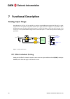
7 func onal descrip on analog input stage input dynamic is 2.25 v pp ; 0.5 v pp and 10 v pp versions are available upon request (see tab. 1.1). In order to preserve the full dynamic range with unipolar input signal, posi ve or nega ve, it is possible to add a dc offset by means of a 16 bit dac, which...
Page 21: Clock Distribution
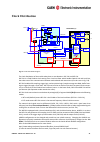
Clock distribution mux osc clk in 50mhz ref-clk trigger & sync logic trg in local bus local bus interface acquisition & memory control logic mezzanines (x2) trigger sync self-trgs mux phase detector ad9520 clk1 sdiv sdiv rdiv refin intclk ctrl ldiv odiv ndiv samp-clk0 fpga (amc) adc ch1 sclk data sy...
Page 22: Pll Mode
Pll mode the phase detector within the ad9520 device allows to couple ref-clk with an internal vcxo, which pro- vides the nominal adcs frequency (100 mhz). As introduced in sec. Clock distribu on, the source of the ref-clk signal (see fig. 7.2) can be external on clk-in front panel connector or inte...
Page 23: Decimation
Decimation this func onality is a firmware op on (amc fpga firmware revision ≥ 0.14) based on the programmability of a decima on factor n. During the acquisi on, the firmware processes the digi zed input waveforms calcula ng an averaged value of the “decimated” 2 n consecu ve samples. The self-trigger ...
Page 24: Acquisition Modes
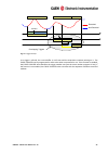
Acquisition modes acquisition run/stop the acquisi on can be started and stopped in different ways, according to bits[2:0] of register 0x8100 [rd1]: - sw controlled (bits[1:0] = 00): start and stop take place by so ware command. Bit[2] = 0 means stopped, while bit[2] = 1 means running. - gpi controll...
Page 25
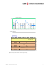
Trigger pre post acquisition window recorded not recorded overlapping triggers event n event n+1 event n+2 fig. 7.3: trigger overlap as a trigger is refused, the current buffer is not frozen and the acquisi on con nues wri ng on it. The event counter can be programmed in order to be either incremente...
Page 26
Multi-event memory organization each channel of the n6724 features a sram memory to store the acquired events. The memory size for the event storage is 512 ks/ch or 4 ms/ch, according to the board version (see tab . 1.1), and it can be divided in a programmable number of buffers, n b (n b from 1 up t...
Page 27: Event Structure
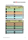
Event structure the event can be readout via usb or op cal link; data format is 32-bit long word (see fig. 7.4). An event is structured as: • header (four 32-bit words) • data (variable size and format) header the header consists of four words including the following informa on: • event size (bits[2...
Page 28
• trigger time tag (bits[31:0] of 4 th header word) is the 31-bit trigger time tag (ttt) informa on (31 bit counter and 32 nd bit as roll-over flag), which is the trigger me reference. If the ettt op on is enabled, then this field becomes the 32 less significant bits of the 48-bit extended trigger time...
Page 29
31 30 29 28 27 26 25 24 23 22 21 20 19 18 17 16 15 14 13 12 11 10 9 8 7 6 5 4 3 2 1 0 event size ch. Mask trigger time tag 1 0 1 0 event counter reserved sample [1] – ch[0] sample [0] – ch[0] sample [3] – ch[0] sample [2] – ch[0] sample [n-1] – ch[0] sample [n-2] – ch [0] sample [1] – ch[1] sample [...
Page 30: Acquisition Synchronization
Acquisition synchronization each channel of the digi zer is provided with a sram memory that can be organized in a programmable number n b of circular buffers (n b = [1 : 1024], see tab. 7.1). When the trigger occurs, the fpga writes further a programmable number of samples for the post-trigger and f...
Page 31: Zero Suppression
Zero suppression in the x724 boards it is possible to select the events according to a ”zero suppression” criterion. The zero suppression allows the user to reduce the amount of data transferred from the board by transferring only the useful informa on. Anyway, since the zero suppression condi on is...
Page 32
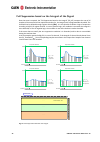
Full suppression based on the integral of the signal once the event is acquired, the ”full suppression based on the integral” (zs_int) compares the sum of all samples of the event within the acquisi on window (i.E. The integral) with a programmable threshold. The threshold can be defined through regi...
Page 33
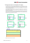
Full suppression based on the amplitude of the signal full suppression based on the signal amplitude (zs_amp) allows the user to discard data from one chan- nel if the signal does not exceed the programmed threshold for at least ns subsequent data. Threshold and ns can be defined through registers 0x...
Page 34: Zero Length Encoding Zle
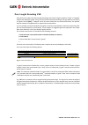
Zero length encoding zle once the event is acquired, the zero length encoding mode is able to tag the samples as ”good” or ”skipped”. Samples are defined as ”good” if they are over/under threshold according to the logic polarity (see bit[31] of register 0x1n24 [rd1]). ”skipped” events are those under...
Page 35
Acquisition window common trigger n lbk ch0 n ovt t zle n lfwd n ovt n lbk n lfwd n skip1 n good1 n skip2 n good2 n skip3 output data: 31 30 29 28 27 26 25 24 23 22 21 20 19 18 17 16 15 14 13 12 11 10 9 8 7 6 5 4 3 2 1 0 size ch0 n skip1 0 reserved n good1 1 reserved samples good1 n skip2 0 reserved...
Page 36
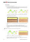
Zle examples this sec on reports some examples of zle. 1. In the simplest case n lbk and n lfwd do not overlap. Fig. 7.9 reports the case of posi ve logic on the le , and nega ve logic on the right. The green areas correspond to the over threshold samples, while the yellow ones correspond to the und...
Page 37
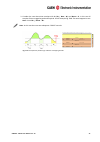
3. Consider the case where n lbk overlaps with n 3 (n 3 ≤ n lbk n 1 ) and n lfwd = 0. In this case all samples of n 3 are tagged as good and acquired. See for example fig. 7.12. The same happens in case n lbk = 0 and n 3 ≤ n lfwd n 5 . Note: in this case there are two subsequent “good” intervals. 31...
Page 38: Trigger Management
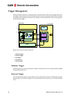
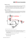
Trigger management when opera ng the waveform recording firmware, all board channels share the same trigger (board com- mon trigger), so they acquire an event simultaneously and in the same way (determined number of samples according to buffer organiza on and custom size se ngs, as well as posi on wit...
Page 39: Self-Trigger
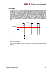
Self-trigger each channel can generate a self-trigger signal (self-trg) when the digi zed input pulse exceeds a config- urable threshold set through the register address 0x1n80 [rd1]. The condi on for the self-trigger genera- on is the pulse to stay under or over the threshold (according to the trigg...
Page 40: Trigger Coincidence Level
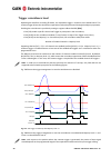
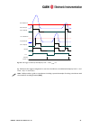
Trigger coincidence level opera ng the waveform recording firmware, the acquisi on trigger is common to the whole board. This common trigger allows the coincidence acquisi on mode to be performed through the majority opera on. Enabling the coincidences is possible by wri ng at register address 0x810c...
Page 41
Ch1 threshold self-trg[ch0] self-trg[ch1] ch0(enabled) in ch0 threshold trigger (maj.Lev = 1) ch1(enabled) in or signal t tvaw fig. 7.16: self-trigger rela onship with majority level = 1 and t tvaw ̸= 0. Fig. 7.17 shows the trigger management in case the coincidences are enabled with majority level ...
Page 42
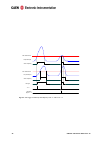
Ch1 threshold self-trg[ch0] self-trg[ch1] ch0(enabled) in ch0 threshold trigger (maj.Lev = 1) ch1(enabled) in or signal t tvaw fig. 7.17: self-trigger rela onship with majority level = 1 and t tvaw = 0. 42 um3247 - n6724 user manual rev. 10
Page 43: Trg-In As Gate
Trg-in as gate it is possible to configure trg-in as a gate for trigger an -veto func on. The common acquisi on trigger is then issued upon the and between the external signal on trg-in and the other trigger sources but the so ware trigger (i.E. The so ware trigger cannot par cipate in the trigger as...
Page 44
Example it could be required to start the acquisi on on all the channels of a mul -board system as soon as one of the board channels (board “n”) crosses its threshold. Trigger out signal is then fed to an external fan out logic unit (e.G. Caen v2495 board); the obtained signal has then to be provide...
Page 45: Test Pattern Generator
Test pattern generator the amc fpga can emulate the adc and write into memory a ramp (0, 1, 2, 3,..Ff, ff, fe.., 0) for test purposes. It can be enabled via register address 0x8000. Reset, clear and default configuration global reset global reset is performed at power-on of the module or via so ware...
Page 46: Block Transfer
Data transfer capabilities and events readout the board features a mul -event digital memory per channel, configurable by the user to be divided into 1 up to 1024 buffers, as detailed in sec. Mul -event memory organiza on. Once they are wri en in the memory, the events become available for readout via...
Page 47
Optical link and usb access the board houses a usb2.0 compliant port, providing a transfer rate up to 30 mb/s, and a daisy chainable op cal link (communica on path which uses op cal fiber cables as physical transmission line) able to transfer data at 80 mb/s, therefore it is possible to connect up to...
Page 48: 8 Drivers & Libraries
8 drivers & libraries drivers in order to interface with the board, caen provides the drivers for the supported physical communica on channels and compliant with windows® and linux® os: • conet op cal link, managed by the a2818 pci card or the a3818 pcie card. The driver installa on package is avail...
Page 49
• caencomm library manages the communica on at low level (read and write access). The purpose of the caencomm is to implement a common interface to the higher so ware layers, masking the details of the physical channel and its protocol, thus making the libraries and applica ons that rely on the caen...
Page 50: 9 So Ware Tools
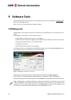
9 so ware tools caen provides so ware tools to interface the 724 digi zer family, which are available for free download at www.Caen.It following the path: home / products / firmware/so ware / digi zer so ware caenupgrader caenupgrader is free so ware composed of command line tools together with a ja...
Page 51: Caencomm Demo
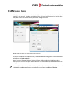
Caencomm demo caencomm demo is simple so ware developed in c/c++ source code and provided both with java™ and labview™ gui interface. The demo mainly allows for a full board configura on at low level by direct read/write access to the registers and may be used as a debug instrument. Fig. 9.2: caencom...
Page 52: Caen Wavedump
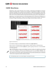
Caen wavedump wavedump is a basic console applica on, with no graphics, suppor ng only caen digi zers running the waveform recording firmware. It allows the user to program a single board (according to a text config- ura on file containing a list of parameters and instruc ons), to start/stop the acquis...
Page 53: Caen Scope
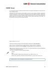
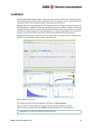
Caen scope in a brand new framework, caenscope so ware allows to manage the caen digi zers running the wave- form recording firmware. Caenscope user friendly interface presents different sec ons to easily manage the digi zer configura on and plot the waveforms. Once connected, the program retrieves the...
Page 54: Caen Mc
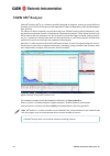
Caen mc 2 analyzer caen mc 2 analyzer (mc 2 a) is a so ware specifically designed for digi zers running the special dpp-pha firmware (724, 725 and 730 families) and the digital mcas (x780 dual digital mca, x781 dual/quad digital mca, dt5770). The so ware is able to completely control and manage a set ...
Page 55: Compass
Compass compass (caen mul -parameter spectroscopy so ware) is the new so ware from caen able to imple- ment a mul -parametric daq for physics applica ons, where the detectors can be connected directly to the digi zers inputs and the so ware acquires energy, ming, and psd spectra. Compass so ware has...
Page 56: 10 Hw Installa On
10 hw installa on • the module fits into all nim crates • use only crates with forced cooling air flow • turn the crate off before board inser on/removal • remove all cables connected to the front panel before board inser on/removal caution: this product needs proper cooling. Use only crates with forc...
Page 57: Power-On Sequence
Power-on sequence to power on the board, perform the following steps: 1. Insert the n6724 into the crate; 2. Power up the crate. Power-on status at power-on, the module is in the following status: • the output buffer is cleared; • registers are set to their default configura on a er the power-on, only...
Page 58: 11 Firmware And Upgrades
11 firmware and upgrades the board hosts one fpga on the mainboard and two fpgas per mezzanine (i.E. One fpga per channel). The channel fpgas firmware is iden cal. A unique file is provided that will update all the fpgas at the same me. Roc fpga mainboard fpga (readout controller + vme interface): fpg...
Page 59: Firmware File Description
Firmware file description the programming file has the extension .Cfa (caen firmware archive). It is an archiving file format that ag- gregates all the programming files of the same firmware kind which are compa ble with the same digi zer family. The cfa naming conven on follows this general scheme: • x...
Page 60: 12 Technical Support
12 technical support caen support services are available for the user by accessing the support & services area on caen website at h p://www.Caen.It. Returns and repairs users who need for product(s) return and repair have to fill and send the product return form (prf) in the returns and repairs area ...
Page 61
Um3247 - n6724 user manual rev. 10- january 27th , 2017 00000-00-02827-gxxx copyright ©caen spa. All rights reserved. Informa on in this publica on supersedes all earlier versions. Specifica ons subject to change without no ce..


