- DL manuals
- Daewoo
- Monitor
- 719B
- Service Manual
Daewoo 719B Service Manual
Summary of 719B
Page 1
Daewoo electronics co., ltd. Http : //svc.Dwe.Co.Kr service manual february, 2001 xga color monitor model : 719b 719bf.
Page 2: Contents
Safety precautions 1 general safety information 2 servicing precautions 3 technical information 6 general information 7 pin connector 8 cautions for adjustment and repair 8 operation and adjustment 9 alignment procedure 15 troubleshooting hints 17 block diagram 33 pcb layout 34 schematic diagram 38 ...
Page 3: Safety Precautions
1 safety precautions ◆ safety check care should be taken while servicing this analog color display because of the high voltages used in the deflection circuits. These voltages are exposed in such areas as the associated flyback and yoke circuits. ◆ fire & shock hazard • insert an isolation transform...
Page 4: General Safety Information
2 general safety information warning: this product includes critical mechanical and electrical parts which are essential for x ray protection. For continued safety, replace critical components that are indicated in the service manual with exact replacement parts given in the parts list. Operating hi...
Page 5: Servicing Precautions
3 servicing precautions ◆ general servicing precautions 1. Always unplug the ac power cord from the ac power source before: a. Removing or reinstalling any component, circuit board, module, or any other instrument assembly. B. Disconnecting or reconnecting any electrical plug or other electrical con...
Page 6
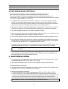
4 ◆ electrostatically sensitive (es) devices some semiconductor (solid state) devices can be damaged easily by static electricity. Such components are commonly called electrostatically sensitive (es) devices. The typical examples of es devices are integrated circuits, some field-effect transistors, ...
Page 7
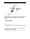
5 figure 1. Use soldering iron to pry leads ◆ ic removal/replacement some utilized chassis circuit boards have slotted (oblong) holes through which the ic leads are inserted and then bent flat against the circuit foil. When holes are slotted, the following technique should be used to remove and repl...
Page 8: Technical Information
6 ◆ power ic, transistor or devices removal/replacement 1. Heat and remove all solders from the device leads. 2. Remove the heatsink mounting screw (if applicable). 3. Carefully remove the device from the circuit board. 4. Insert new device in circuit board. 5. Solder each device lead and then clip ...
Page 9: General Information
Adj adjustment afc automatic frequency control crt cathode ray tube def deflection d.Y deflection yoke fbt flyback transformer h.Sync horizontal synchronization osc oscillator p.S.U power supply unit pwa printed circuit board wiring assembly r.G.B red, green, blue v.Sync vertical synchronization 7 g...
Page 10: Pin Connector
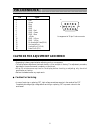
Pin signal 1 red 2 green 3 blue 4 gnd 5 gnd 6 gnd - red 7 gnd - green 8 gnd - blue 9 +5vdc 10 gnd - h.Sync 11 gnd - v.Sync 12 bi-directional data (sda) 13 horizontal sync 14 vertical sync (vclk) 15 data clock (scl) 8 pin connector • degaussing is always required when adjusting purity or convergence....
Page 11: Operation and Adjustment
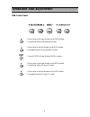
9 operation and adjustment 719b control panel • move cursor to the right window on the osd window . • increase the value of any selected function. • move cursor to the left window on the osd window. • decrease the value of any selected function. • launch osd(on-screen display) menu window. • move cu...
Page 12
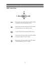
10 719bf control panel • move cursor to the right window on the osd window . • increase the value of any selected function. • move cursor to the left window on the osd window. • decrease the value of any selected function. • launch osd(on-screen display) menu window. • move cursor to the high window...
Page 13
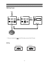
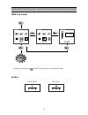
11 719b key process • when you choose the icon on the osd window, you can exit the osd screen. Hot key brightness contrast osd off menu menu menu menu.
Page 14
12 719bf key process • when you choose the icon on the osd window, you can exit the osd screen. Hot key brightness contrast osd off.
Page 15
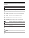
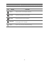
13 osd functions adjust the parallelogram when the screen is leaning left or right. Parallelogram adjust the trapezoid of the screen by moving the lines inward or outward. Adjust the side balance when the sides of the screen are bowed towards left or right. Pin balance trapezoid degauss the display ...
Page 16
14 select language for osd (5 languages). Language icon control functions reset the screen to the factory preset display settings. Recall adjust the vertical picture moire cancellation. V. Moire adjust the horizontal picture moire cancellation. H. Moire display horizontal & vertical frequency and po...
Page 17: Alignment Procedure
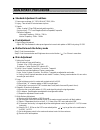
◆ standard adjustment conditions 1. Power source voltage : ac 120v, 60hz/ac 220v, 50hz. 2. Aging : take at least 20 minutes warm-up time. 3. Signals. Video : analog 0.7vpp 75 Ω terminal positive polarity synchronizing : ttl level negative/positive separate/composite deflection frequency horizontal f...
Page 18
16 (h) select the r, g, b gain on the osd menu and adjust the / key to get the color coordinates in x=0.281±0.02, y=0.311±0.02. (i) adjust the sub contrast control to get the screen luminosity to 32ft/l. 6. Static convergence adjustment (a) apply a magenta cross hatch pattern on display. (b) adjust ...
Page 19: Troubleshooting Hints
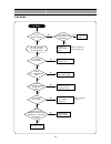
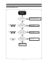
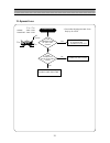
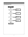
17 troubleshooting hints 1. No character are the contrast & brightness controls maximum change the contrast & brightness control to maximum no raster refer to no raster check the peripheral circuit of crt board check the video output (ic802, tda9536) and their ambient circuit trouble in 6.3vdc line ...
Page 20
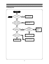
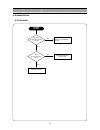
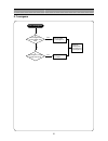
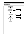
18 2. No raster trouble in power supply circuit trouble in power supply circuit trouble in g1 line of main pwb trouble in fbt or peripheral circuit high voltage trouble in fbt trouble in 100vdc line of power supply unit refer to trouble in p.S.U refer to trouble in power supply unit. Is crt heater r...
Page 21
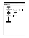
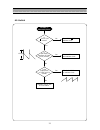
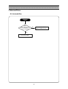
19 3. A missing color is input signal normal? One color is missing crt cathode (rk, gk, bk) is normal? Is video output ic(ic802, tda9536) normal? Each grid (g1, g2) voltage normal? Is the output of pre-amp (ic801, tda9210) pin 16,18, 20 all normal? Check video signal cable or video card. Trouble in ...
Page 22
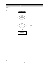
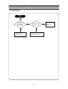
20 4. Abnormal osd font is menu key selected? Is osd font exist? * if menu key selected. Is +5v voltage about 5v? Abnormal osd font is the output of ic803 (pin 13, 14, 15) normal? Trouble in +5v voltage line. Refer to trouble in p.S.U troubie in ic803 or its ambient circuit trouble in ic803 and its ...
Page 23
21 5. Horizontal output circuit is the b+line voltage over 45v? Is the h-out waveform of ic501 normal? Trouble in b+ booster circuit (check the b+section of ic501) trouble in ic501 trouble in horizontal output circuit (no raster yes no is the collector wave form of q504 normal? Yes yes yes trouble i...
Page 24
22 6. Unstable picture 6-1. Horizontal unstable picture is h.Sync input pin of ic501 correct? Check h.Sync out of micom or its ambient circuits. Is the pin 10 of ic501 12v? Check the value of c513, r522 yes yes no no trouble in ic501.
Page 25
23 6-2. Vertical unstable or abnormal picture is 13v dc line correct? Check pwr 13v ambient circuit. No yes is the output waveform of ic401 (pin 6) normal? Trouble in v.Sync line or ic501 failure. Yes no 45vp-p is the output pulse of ic501 (pin 23) normal? Yes no check v.Dy and ambient circuit. Chec...
Page 26
24 7. Focus monitor remains unfocused check focus vr in fbt is focus acceptable? Trouble in focus circuit (fbt) yes ok no.
Page 27
25 7-1. Dynamic focus focus is poor is the waveform of the df pin in fbt correct? Orion : 300v 120v samsung : 300v 120v 1. Check the crt socket or connector wire 2. Trouble in fbt or crt * check after adjusting the static focus finely by vr in fbt df waveform f vh f vh f vv f vv no yes is the wavefo...
Page 28
26 8. Convergence is convergence on the center area bad? Is convergence on the fringe area bad? Adjust static convergence refer to adjustment procedure of convergence yes adjust d.Y location yes no poor convergence.
Page 29
27 9. Abnormal picture 9-1. Horizontal size when the h.Size on the osd is changed, is the h.Size changed? No yes check pin 11 of ic501 and its ambient circuit it isn’t out of order. Abnormal h.Size.
Page 30
28 9-2. Vertical size is changeable the dc voltage of ic401 pin 6? Check the ic401 and its ambient circuit check the pin 23 of ic501 and its ambient circuit no no trouble v.Osc/ deflection circuit refer to v.Osc/deflection circuit yes is the 3.5vdc of pin 23 of the ic501? Yes abnormal v.Size.
Page 31
29 10. High voltage output circuit trouble in fbt is q505 collector waveform normal? Yes yes no trouble in ic501 ambient circuit is ic501 pin 8 normal? Yes no trouble in h.V circuit (no raster) trouble in ic501 ambient circuit is the ic501 pin15 h.Trigger correct? Yes no trouble in h.Trigger trouble...
Page 32
30 11. Side-pincushion circuit side-pincusion distortion is excessive or barrel o.K select the side-pincushion icon on osd menu, and adjust acceptable position. Yes check ic803 or their ambient circuit is the pin 5,10 waveform of ic803 correct? Yes no check ic803or it’s ambient circuit. Trouble in h...
Page 33
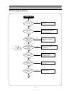
31 12. Power supply unit (p.S.U) trouble in p.S.U is power switch on? Switch on no yes yes is fuse f001 o.K? Check the power cord outlet and diode d001, d002, d003, d004, q001 no is voltage of c102 100vdc? Trouble in d101 or video part no is voltage of c105 8vdc? Trouble in d103 no is voltage of t00...
Page 34
32 is voltage of c106 27vdc? Trouble in d108 no is voltage of c109 13vdc? No yes yes yes is voltage of c108 -13vdc? Trouble in d104 or vertical part p.S.U o.K trouble in d106 or horizontal part no a.
Page 35: Block Diagram
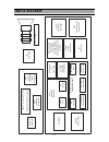
33 block diagram crt socket crt : orion mini -neck 15" d -sub rgb h/v video pre - amp (65m h z ) tda9210 (sgs thompson) os d nt6828 (novatek) crt d river tda9536 (sgs thompson) ac input smps transformer mcu nt68p62 (novatek) h /v osc processor tda4856 (philip s ) v - driver ka2142b (samsung) pwm d/a...
Page 36
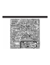
Pcb layout 34 719b/719bf main pcb component side.
Page 37
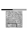
35 719b/719bf main pcb solder side.
Page 38
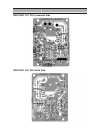
36 719b/719bf crt pcb solder side 719b/719bf crt pcb component side.
Page 39
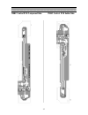
37 719bf control pcb solder side 719bf control pcb component side.
Page 40
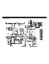
38 power & connection section schematic diagram.
Page 41
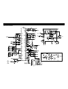
39 control & vert. Out section.
Page 42
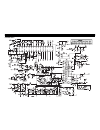
40 horizontal section.
Page 43
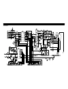
41 video section.
Page 44
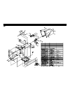
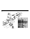
42 exploded view & mechanical parts list 719b 719b.
Page 45
719b 719bf 43.
Page 46: Electrical Parts List
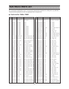
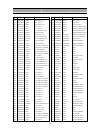
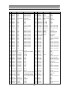
C210 ccxb1h181k c cera 50v b 180pf k (tapping) c211 ccxb1h181k c cera 50v b 180pf k (tapping) c212 ccxf1h104z c cera 50v f 0.1mf z c213 ccxf1h104z c cera 50v f 0.1mf z c221 ccxf1h104z c cera 50v f 0.1mf z c223 ccxf1h104z c cera 50v f 0.1mf z c405 cexf1c102v c electro 16v rss 1000mf (10x20) tp c406 c...
Page 47
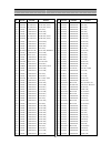
46 c546 cmxm2a682j c mylar 100v 6800pf j (tp) c548 ccxf1h104z c cera 50v f 0.1mf z c549 cmxm2a152j c mylar 100v 1500pf j (tp) c550 ccxf1h104z c cera 50v f 0.1mf z c551 ccxf1h104z c cera 50v f 0.1mf z c552 cmyf2d125j c mylar mpp 200v 1.2mf j bulk c553 cmxl2e104j c mylar meu 250v 0.1mf j c596 cmxm2a10...
Page 48
47 d514 drgp10d--- diode rgp 10-d (tapping) d515 dzn4148--- diode 1n4148 auto 52mm d517 dzn4148--- diode 1n4148 auto 52mm d518 rd-az331j- r carbon film 1/6 330 ohm j d519 dzn4148--- diode 1n4148 auto 52mm d521 d1n4007--- diode in4007 d522 d1n4007--- diode in4007 d523 d1n4007--- diode in4007 d560 drg...
Page 49
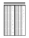
48 r001 rc-2z684j- r carbon comp 1/2 680k ohm j r003 rs01z513js r m-oxide film 1w 51k ohm j small r004 rs01z513js r m-oxide film 1w 51k ohm j small r005 rd-az102j- r carbon film 1/6 1k ohm j r007 rd-az333j- r carbon film 1/6 33k ohm j r008 rd-az472j- r carbon film 1/6 4.7k ohm j r009 rs02z683js r m-...
Page 50
49 r521 rd-az471j- r carbon film 1/6 470 ohm j r522 rd-az122j- r carbon film 1/6 1.2k ohm j r523 rd-2z221j- r carbon film 1/2 220 ohm j r524 rs02z680js r m-oxide film 2w 68 ohm j small r525 rs02z240js r m-oxide film 2w 24 0hm j small r526 rd-2z229j- r carbon film 1/2 2.2 ohm j r527 rd-az222j- r carb...
Page 51
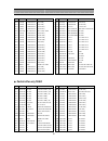
50 r862 rd-az330j- r carbon film 1/6 33 ohm j r863 rd-az360j- r carbon film 1/6 36 ohm j r864 rd-4z201j- r carbon film 1/4 200 ohm j r865 rd-4z121j- r carbon film 1/4 120 ohm j r866 rs01z519js r m-oxide film 1w 5.1 ohm j small r871 rd-az101j- r carbon film 1/6 100 ohm j r880 rd-az123j- r carbon film...
Page 52
Daewoo electronics co., ltd 686, ahyeon-dong mapo-gu seoul, korea c.P.O. Box 8003 seoul, korea telex : dwelec k28177-8 cable : "daewooelec" e-mail : djkoo@web.Dwe.Co.Kr.


