- DL manuals
- Daewoo
- DVD Player
- DG-K301
- Service Manual
Daewoo DG-K301 Service Manual
Summary of DG-K301
Page 1
July. 2007 service manual dg-k301 ✔ caution : in this manual, some parts can be changed for improving, their performance without notice in the parts list. So, if you need the latest parts information,please refer to ppl(parts price list) in service information center. Dvd player model:.
Page 2
Contents contents specifications.........................................................................................................................2 circuit operational description.........................................................................................3 voltage charts............
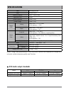
Page 3: Dvd Audio Output Standards
2 laser wavelength 650nm video pal/auto/ntsc frequency response 20hz ~ 20khz (±db) signal/noise ratio ≥90db channel separation ≥85db ( khz) dynamic range ≥80db ( khz) output audio analog output level : 2.0 + 0/-0.2vrms (load impedance : ,0kΩ) digital output level : 0.5 ±0.Vp-p (load impedance : 75Ω)...
Page 4
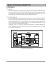
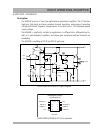
3 1. Dvd module ) summary dvd one board consists of: loader part that reads and transmits audio and video data saved at optic discs (dvd, cd-da, vcd, cd-r) to mpeg decoder part; mpeg decoder part, which, by decoding and encoding data received from the loader, produces analog signals; and u-com that ...
Page 5
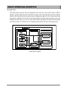
4 circuit operational description circuit operational description 3) loader part the loader which read the data of audio/video from optic disc and transfer them to mpeg decoder can be divided into deck total dvd assay(in a short term, mecha) and servo. Mecha mounts with the optical pick-up which all...
Page 6: S5L500
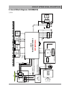
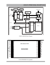
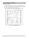
5 circuit operational description 2. Overall block diagram--s5l5008(2ch) ) 2ch m m d is c sp in d le m o to r lo a d ing m o to r dec k m ech ani sm d v d : a ,b ,c ,d ,r f cd : a, b,c ,d ,e,f,r f p d ,p r e f pick u p k ey in pu t b /p b ic 10 1 29 lv 80 0 8m fl a sh r o m fd a[0 :20 ] nso e nsc so...
Page 7
6 circuit operational description 3. Mpeg decoder the signal read from dvd disc is output into the rf signal and servo related signal through the rf ic and they are input into the mpeg decoder and processed the mpeg decoding and divided into video/audio signal. The video signal is output into the an...
Page 8
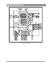
7 circuit operational description s5l5008 block diagram i2 c ir uart g pi o 16 bi tt im er s w d t c lk r st _g en pl ls jt a g pc de bu gg er ex ti n t/ u se ri f spdif master xt l d eb ug ge r 32-bit apb 32 -b it a h b s mpeg video decoder bus bridge sub-picture decoder ntsc /pal encoder miu/arbit...
Page 9
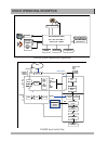
8 circuit operational description s5l5008 system diagram(servo application) s5l5008 servo control flow deck mechanism p/u s5l5008x(dvdp soc) cpu + rf + servo/dsp + a/v decoder + dram 2-ch dac 5.1-ch dac display sdram flash rom peripherals front vfd display (spi interface) ir key display audio amp vr...
Page 10
9 circuit operational description s5l5008 h sy n c (p 0. 5) m d b1 2 vd d p4 vs sp 5 m d b3 m d b1 3 m d b2 m d b1 4 m d b1 m d b1 5 vd d c 2 vs sc 2 m d b0 vs sp 6 n tp st (p 0. 0) vd d 5 vd d c 3 vs sc 3 td i(p 0. 1) tc k( p0 .2 ) tm s( p0 .3 ) td o (p 0. 4) vs yn c (p 0. 6) bt c lk (p 0. 7) d ac ...
Page 11
0 circuit operational description 2) flash memory : es29lv800db-70tg description the es29lv800 is a 8 megabit, 3.0 volt-only flash memory device, organized as m x 8 bits (byte mode) or 52k x 6 bits (word mode) which is configurable by byte#. Four boot sectors and fifteen main sectors are provided : ...
Page 12: Es29Lv800
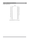
Circuit operational description flash es29lv800 block diagram a15 a14 a13 a12 a11 a10 a9 a8 nc nc we# reset# nc nc ry/by# a18 a17 a7 a6 a5 a4 a3 a2 a1 a16 byte# vss dq15/a-1 dq7 dq14 dq6 dq13 dq5 dq12 dq4 vcc dq11 dq3 dq10 dq2 dq9 dq1 dq8 dq0 oe# vss ce# a0 1 2 3 4 5 6 7 8 9 10 11 12 13 14 15 16 17 ...
Page 13
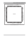
2 circuit operational description 3) sdram : mmsd46t26-o sdrom mmsd46t26-o pin assignments.
Page 14
3 circuit operational description 4) amplifiers : az4558cm-e description the az4558 consists of two high performance operational amplifiers. The ic features high gain, high input resistance, excellent channel separation, wide range of operating voltage and internal frequency compensation. It can wor...
Page 15
4 circuit operational description 5) motor drive ic: at5669 the at5669 is a 5-channel btl driver ic. Two of them can drive dc motors and two can drive coils, such as the focus and tracking actuators of a cd-rom/dvd-rom/dvd-player system it also built-in one channel bi-direction dc motor driver for t...
Page 16
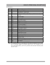
5 circuit operational description pin descriptions pin no. Pin name function in ch(focus coil) input 2 dl linear regulator 3v3 driver output 3 fb2 linear regulator 2 feedback input 4 in2 ch2(sled driver) input 5 3v3 linear regulator 3v3 input(metal option possible for other voltage from 2.5v~4v) 6 f...
Page 17
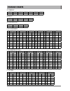
6 voltage charts u sm8002c pin 2 3 4 5 6 voltage 0.372v 0.76v .734v .742v 20.2v .965v u2 el87 pin 2 3 4 voltage 0.483v 3.88v 0.237v 2.637v u3 az43bz-atre pin r a k voltage 2.476v 0v 3.82v ic0 es29lv800d voltage voltage voltage voltage voltage voltage pin stop play pin stop play pin stop play pin sto...
Page 18
7 voltage charts ic304 az4558cm-e voltage voltage voltage voltage pin stop play pin stop play pin stop play pin stop play 1 0v 0v 3 0v 0v 5 0v 0v 7 0v 0v 2 0v 0v 4 .7v .7v 6 0v 0v 8 0v 0v ic00 s5l5008 voltage voltage voltage voltage voltage voltage pin stop play pin stop play pin stop play pin stop ...
Page 19
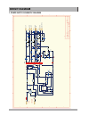
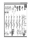
8 circuit diagram 1. Power supply schematic diagram 1 2 3 4 6 5 a b c d 6 5 4 3 2 1 d c b a ti tle noi siv er re b mu n si ze b fo t ee hs 70 02- be f-3 1 :et a d d ra w n by : u 2 pc 81 7c u 3 tl 43 1 r1 0 22 0r c1 1 22 4/ 50 v 2 c9 33 0u f/ 10 v po rt g n d c1 7 10 3/ 50 v u 2 pc 81 7 r4 10 0k /1 ...
Page 20
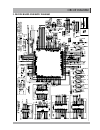
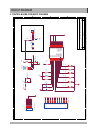
Circuit diagram 9 2. Decode board schematic diagram.
Page 21
Circuit diagram 20
Page 22
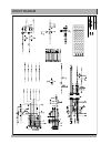
Circuit diagram 2.
Page 23
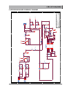
Circuit diagram 22 3. Control board schematic diagram 5 5 4 4 3 3 2 2 1 1 d d c c b b a a sensor remote open/close play re wo p po ts re al s ta bd y se le ct next prev 1. 1 a 85 0 g v g c gvg-679(standby) control borad sechmatic a4 1 2 wednesday, june 06, 2007 titl e ve r re b mu n t ne mu co d ezi...
Page 24
Circuit diagram 23 4. Microphone board schematic diagram 5 5 4 4 3 3 2 2 1 1 d d c c b b a a a1.0 2399 karaoke schematic a3 1 1 tuesday, april 03, 2007 g vg d ig it a l te c h n o lo g y lt d ..C o title ve r re b mu n t ne mu co d ezi s te eh s :et a d of 0 0 0 0 0 0 0 0 0 0 0 0 0 0 0 0 0 r2 6 1k c...
Page 25
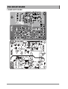
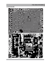
24 pcb circuit board 1. Power supply board.
Page 26
Pcb circuit board 25 2. Decode board.
Page 27
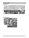
Pcb circuit board 26 3. Control board 4. Microphone board.
Page 28
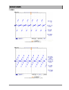
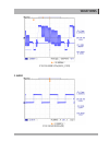
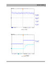
27 waveforms 1. Video ic00 s5l5008 85pin (dac0) ic00 s5l5008 86pin(dac_pb).
Page 29
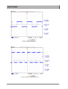
Waveforms 28 ic00 s5l5008 87pin(dac2_y) ic00 s5l5008 90pin(dac3_c).
Page 30
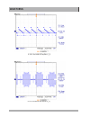
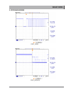
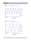
Waveforms 29 ic00 s5l5008 9pin(dac4_cvbs) 2. Audio c00 s5l5008 95pin(fr).
Page 31
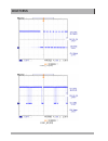
Waveforms 30 ic00 s5l5008 96pin(fl) ic00 s5l5008 08pin(spdif_r).
Page 32
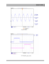
Waveforms 3 3. System waveforms con_4p(ir) con_6p(daio).
Page 33
Waveforms 32 con_7p(clk) con_8p(stb).
Page 34
Waveforms 33 con2_7p(rf) nsys_reset_3.3v.
Page 35
Waveforms 34 sdram clk crystal 4mhz.
Page 36
Waveforms 35 crystal 27mhz ic 7pin,6pin_open_close.
Page 37
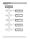
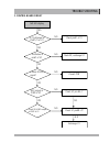
36 trouble shooting 1. Power circuit yes yes yes yes yes n o n o n o n o no power power cord is ok exchange power card (+) voltage of c1,c2 check f1, l1, d1~d4 switching waveform of u1 cheack u1,u2,u3,d5 output voltage of d7~d9 replace bad parts check other parts no check l3,l4.
Page 38
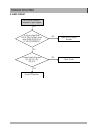
Trouble shooting 37 2. Control board circuit yes yes yes yes yes no no no no no yes n o no led display is 5v obtained at pin#7,21 of u1 check pin#1 of j1 oscillation at pin#1 of u1 check r2, exchange u1 is there key/seg signal? Cheack pcb key output at port of u1 check u1 pin #6~7 check seg/grid out...
Page 39
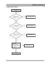
Trouble shooting 38 3. Video circuit yes yes yes no no no cvbs & s-vidro & com p onent signal appear is signal output from adc0~dac4 of net; check pin# 85,86,87,90,91 of ic100 (s5l5008a01) check mpeg system module is signal output from part q5, q6, q7, q8, q9 ,q15 check triode check pcb pattern.
Page 40
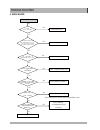
Trouble shooting 39 4. Audio output circuit yes yes yes yes n o n o n o no no sound audio signal from pin#96,97 of ic100 replace the ic100 check audio op amp ic304 pin#1,7 check inserted part: check pattern is there mode(l) at pin#107 of ic100? Check parts: check output jack c348,r349,q350, c351,r35...
Page 41
Trouble shooting 40 5. Mpeg board yes no yes no yes no yes no yes no no no check soldering or replace it +1.2v regulator(q14pin2) check +3.3v regulator(q13 pin2) check that voltage is between 3.3v-3.5v that voltage is between 1.2v-1.3v check all connectors con7 check +5v (pin4,6) check power circuit...
Page 42
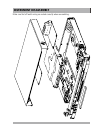
4 instrument disassembly make sure that all leads/ wiring are routed correctly when reassembling..
Page 43: Set Material List
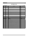
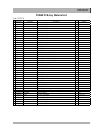
42 partslist set material list code: 6020892 no part code part name description qty location 6020892 dvd player dg-k30-s5l5008,shinwa,2.0ch,2mic,yuv 2 090004 battery 7# english lead free no hg(r03 um-4) 2 3 30584 conn wire 2.0 two heads p*80mm,, red white conn wire ,same direction 4 35048 power cord...
Page 44: Mpeg Pcb Assy Material List
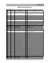
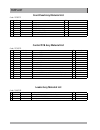
Partslist 43 mpeg pcb assy material list code: 5700423 no part code part name description qty location 5700423 m p e g p c b assy gv-djas5l5008-msam00--26(2.0ch) coaxial,optical,s-video,mic,yuv 2 005000 r chip /6w,0e,±5%,0603 22 r7,r0,r46,r47,r69,r78,r79,r02,r63,r58,r77,r9[2m x6sdram(r92,r97)o type,...
Page 45
Partslist 44 no part code part name description qty location 46 0200023 c chip 562,50v,±0%,0603 c23 47 0200036 c chip 04,50v,±0%,0603 4 bc9~bc2 48 020004 c chip 52,50v,±0%,0603 2 c7,c2 49 0200042 c chip 82,50v,±0%,0603 2 c4,c5 50 020009 c chip 224,25v,±0%,0603 2 c,c2 5 0200092 c chip 05,25v,±0%,0603...
Page 46
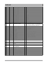
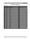
Partslist 45 power pcb assy material list code: 57505 no part code part name description qty location 0000004 r carbon film /6w,4.7k,±5%,tp 3 r2,r3,r4 2 0000099 r carbon film w,00k,±5%,tp r4 3 00008 r carbon film /8w,0e,±5%,tp r9 4 00002 r carbon film /8w,k,±5%,tp r3 5 000023 r carbon film /8w,m,±5%...
Page 47: Loader Assy Material List
Partslist 46 front panel assy material list code: 578073 no part code part name description qty location 200053 panel dg-k30 2 200348 knob gvg-679 power knob 3 200349 knob gvg-679 function knob 4 242075 fittings gvg-679-2 left fittings 5 242076 fittings gvg-679-2 right fittings 6 3500004 screw btpw3...
Page 48: Mic Pcb Assy Material List
Partslist 47 mic pcb assy material list code: 570097 no part code part name description qty location 0000004 r carbon film /6w,4.7k,±5%,tp r7 2 0000005 r carbon film /6w,0k,±5%,tp 7 r22,r23,r3,r4,r5,r6,r2 3 000003 r carbon film /6w,.5k,±5%,tp r3 4 000004 r carbon film /6w,5.6k,±5%,tp r 5 000005 r ca...


