- DL manuals
- Daewoo
- DVD Player
- DHC - 2300K
- Service Manual
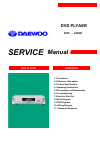
Daewoo DHC - 2300K Service Manual
Summary of DHC - 2300K
Page 1
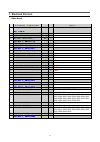
Dvd plyaer dhc - 2300k service manual dvd player contents 1. Precautions 2. Reference information 3. Product specification 4. Operating instructions 5. Disassembly and reassembly 6. Troubleshooting 7. Electrical part list 8. Block diagram 9. Pcb diagrams 10. Wiring diagram 11. Schematic diagrams.
Page 2: 1. Precautions
2 1) before returning an instrument to the customer, always make a safety check of the entire instrument, including, but not limited to, the following items: (1) be sure that no built-in protective devices are defective or have been defeated during servicing. (1) protective shields are provided to p...
Page 3
3 (5) within the limits specified, there is the possibility of a shock hazard, and the instrument must be re-pared and rechecked before it is returned to the customer. See fig. 1-2. Fig. 1-2 insulation resistance test 2) read and comply with all caution and safety related notes non or inside the cab...
Page 4
4 caution : before servicing instruments covered by this service manual and its supplements, read and follow the safety precautions section of this manual. Note : if unforeseen circument create conflict between the following servicing precautions and any of the safety precautions, always follow the ...
Page 5
5 electrostatically sensitive devices (esd) some semiconductor (solid state) devices can be damaged easily by static electricity. Such components commonly are called electrostatically sensitive devices(esd). Examples of typical esd devices are integrated circuits and some field-effect transistors an...
Page 6: 2. Reference Information
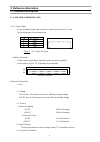
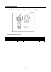
6 * d.C. Power supply a 4-pin shrouded, keyed male connector is used to provide the d.C. Power. The pin assignment is described below. Pin dc volts 1 +12v 2 gnd 3 gnd 4 +5v figure-1 d.C. Power connector * interface connector a 39-pin male, unshielded, shrouded, keyed connector are applied. Please re...
Page 7
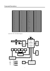
7 i/f signals i/o pin # i/f signals i/o pin # reset 1 dmarq 21 gnd 2 gnd 22 dd7 3 diow 23 dd8 4 gnd 24 dd6 5 dior 25 dd9 6 gnd 26 dd5 7 iordy 27 dd10 8 csel 28 dd4 9 dmack 29 dd11 10 gnd 30 dd3 11 intrq 31 dd12 12 iocs16 32 dd2 13 da1 33 dd13 14 pdiag 34 dd1 15 da0 35 dd14 16 da2 36 dd0 17 cs1fs 37 ...
Page 8
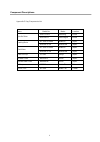
8 appendix 2. Key-components list items model no. Maker location dmdspc41c samsung korea spindle motor rsm-2811f samhongsa korea rf-300ca-11440 mabuchi japan loading motor mdn3bl3csa matsushita japan rf-300ca-11440 mabuchi japan sled motor mdn3bl3csa matsushita japan laser pick-up sf-hd3 sanyo japan...
Page 9
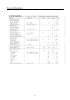
9 * recommended operating conditions item symbol min. Typ. Max. Unit supply voltage vcc 4.75 5.0 5.25 v high level input voltage vih 2.0 - vcc v low level input voltage vil 0 - 0.8 v component descriptions 2-1-2 fiber optic transmitting module for digital audio eqipments (totx178).
Page 10
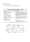
10 component descriptions 2-1-3 ntsc/pal digital video encoder (adv7170).
Page 11
11 comonent descriptions ma.
Page 12
12 comonent descriptions.
Page 13
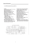
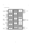
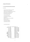
13 * features l single-chip dvd video decoder in a 208-pin pqfp package l supports mpeg-1 system and mpeg-2 program streams l programmable multimedia processor architecture l compatible with audio cd, video cd, vcd 3.0, and super video cd(svcd) l dvd navigation 1 l built-in content scrambling system...
Page 14
14 * functional description component descriptions.
Page 15
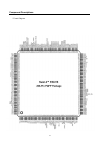
15 component descriptions * pinout diagram.
Page 16
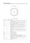
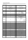
16 *pin description name number i/o definition vcc 1, 9, 18, 27, 35, 44, 51, 59, 68, 75, 83, 92, 99, 104, 111, 121, 130, 139, 148, 157, 164, 172, 183, 193, 201 i 3.65 v ± 150 mv. La[21:0] 23:19,16:10,7:2,207:204 o device address output. Vss 8,17,26,34,43,52,60,67,76,84,91,98,103, 112,120,129,1 38,14...
Page 17
17 component descriptions name number i/o definition hsynch# 119 i/o horizontal synch for screen video interface, programmable for rising or falling edge, active low. Hd[15:0] 141:140, 137:131, 128:122 o host data bus hcs1fx# 152 o host select 1. Hcs3fx# 153 o host select 3. Hiocs16# 151 i device 16...
Page 18
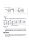
18 component descriptions 2-1-5 digital-to-analog stereo audio converter (cs4391).
Page 19
19 component descriptions.
Page 20
20 component descriptions.
Page 21
21 component descriptions.
Page 22
22 component descriptions 2-1-6 digital-to-analog stereo audio converter (cs4340).
Page 23
23 component descriptions.
Page 24
24 component descriptions.
Page 25
25 absolute maximum ratings power suppiy voltage……………………………6.0v input current………………………………………15ma power dissipatron…………………………………75mw operating temperature range………………….-55~+125 ° c storage tenperature……………………………..-65~+150 ° c component descriptions.
Page 26
26 * features fully static design 8-bit cmos microcontroller 256 bytes of on-chip scratchpad ram 8 kb electrically erasable/programmable mtp-rom 64 kb program memory address space 64 kb data memory address space four 8-bit bi-directional ports three 16-bit timer/counters one full duplex serial port(...
Page 27
27 component descriptions * pin description symbol descriptions ea# external access enable: this pin forces the processor to execute out of external rom. It should be kept high to access internal rom. The rom address and data will not be presented on the bus if ea pin is high and the program counter...
Page 28
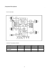
28 * block diagram * absolute maximum ratings parameter symbol min. Max. Unit dc power supply vdd-vss -0.3 +7.0 v input voltage vin vss -0.3 vdd +0.3 v operating temperature ta 0 70 °c storage temperature tst -55 +150 °c component descriptions.
Page 29
29 * features • low-voltage and standard-voltage operation – 5.0 (v cc = 4.5v to 5.5v) – 2.7 (v cc = 2.7v to 5.5v) – 2.5 (v cc = 2.5v to 5.5v) – 1.8 (v cc = 1.8v to 5.5v) • internally organized 128 x 8 (1k), 256 x 8 (2k), 512 x 8 (4k),1024 x 8 (8k) or 2048 x 8 (16k) • 2-wire serial interface • schmi...
Page 30
30 component descriptions * features • 5.0v±40% for read and write operations • access time –70max • current –20 ma typical active read current –30 ma typical program/erase current –1µa typical cmos standby • flexible sector architecture – 8 uniform sectors of 64 kbyte each – any combination of sect...
Page 31
31 block diagram * absolute maximum ratings* ambient operating temperature ...................... -55°c to +125°c storage temperature ...................................…. -65°c to +150°c voc ground .……………………………………..-2.0v to +7.0v output voltage…………………………………… -2.0v to +7.0v component descriptions.
Page 32
32 features n jedec standard 3.3v power supply n lvttl compatible with multiplexed address n dual banks / pulse ras n mrs cycle with address key programs - cas latency (2,3) - burst length (1,2,4,8 & full page) - burst type (sequential & interleave) n all inputs are sampled at the positive going edg...
Page 33
33 component descriptions block diagram pin descriptions symbol name description clk system clock active on the positive going edge to sample all inputs. Cs chip select disables or enables device operation by masking or enabling all inputs exceptclk, cke and l(u)dqm cke clock enable masks system clo...
Page 34: 3. Product Specifications
34 n playback system dvd video video cd (1.1, 2.0, 3.0) svcd and cvd cdda cd-rom with mp3 data n television signal system ntsc/pal n video performance video out 1 vpp into 75 ohm s-video out y : 1 vpp into 75 ohm c : 0.286 vpp into 75 ohm component out 0.7 vpp into 75 ohm d/a converter 27mhz / 10bit...
Page 35
35 n connections coaxial digital out x1 audio analog out for 2-channel x1 scart connector for component video x1 scart connector for external video x1 (option) composite video out x1 s-video out x1 optical out x1 n power supply power source ac 90~250v, 50/60hz power consumption n set dimensions (w x...
Page 36: 4. Operating Instructions
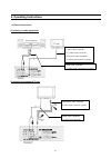
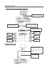
36 connecting to audio equipment connecting to a monaural tv set 4. Operating instructions 4-1 basic connections audio equipment tv set audio cable (optional) to audio input connector (red, white) s-video cable (optional) to s-video input connector video/audio cable (supplied) to video input connect...
Page 37
37 connecting to a stereo tv set connecting to a decoder with a dolby digital or dts processing tv set video/audio cable (supplied) coaxial audio cable (optional) to coaxial digital audio input optical audio cable (optional) to optical digital audio input decoder or amplifier with dolby digital / dt...
Page 38
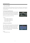
38 press setup button and select video submenu on setup screen. After that, select tv type by pressing down arrow button ( ▼) until desired tv mode is selected. For more information, refer to 7.2 video on the instruction manual. When a dvd disc is loaded, select desired menu item using arrow button ...
Page 39
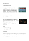
39 use arrow button and select an mp3 title using the select button then play will start automatically. When you know the title number, enter the mp3 title number using numeric buttons and press the se- lect button. If you want to play an adjacent mp3 title, press the next button for next title and ...
Page 40
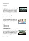
40 when you want to view the disc contents very slowly in forward or reverse direction, you can do that by pressing the ff/sf button ( ) or the fr/sr button ( ) during pause mode. There are total 3 steps for dvd and vcd. They are slow 1/2x, slow 1/4x and slow 1/8x for both direction. The slow revers...
Page 41
41 some dvd discs may contain scenes, which have been shot simul- taneously from a number of different angles. If the loaded disc su- pports multiple angles, you can see indicator on the fluorescent display and the tv screen. In the figure shown right, there are total 9 angles. To switch to the angl...
Page 42: Remained to Be Defined
42 operating instructions remained to be defined.
Page 43
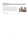
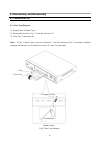
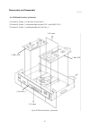
43 1) supply power and open tray ¶. 2) disassemble the door tray · in direction off arrow “a”. 3) close tray ¶ and power off. Note : if tray ¶ doesn’t open, insert a screw driver ¹ into the emergency hole ¸ (as shown in detailed drawing) and then turn it in the direction of arrow “b”. Open tray manu...
Page 44
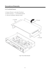
44 1) remove 3 screws ¶ on the back top cabinet. 2) remove 2 screws ·, ¸ on the left and right side. 3) lift up the top cabinet in direction of arrow. Disassembly and reassembly 5-1-2 top cabinet removal · 2 screws ¶ 3 screws ¸ 2 screws fig 5-2 top cabinet removal.
Page 45
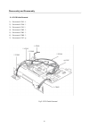
45 1) disconnect pcn1 ¶. 2) disconnect pcn4 ·. 3) disconnect lcn1 ¸. 4) disconnect con2 ¹. 5) disconnect con1 º. 6) disconnect con6 ». 7) disconnect lcn7 ○ 7 . 5-1-3 pcb cable removal disassembly and reassembly ¶ pcn1 · pcn4 ○ 7 lcn7 ¹ con2 º con1 fig 5-3 pcb cable removal ¸ lcn1 º con6.
Page 46
46 1) remove 2 screws ¶ on the back of the cabinet. 2) remove 8 screws · and disassemble the main pcb ¹ and smps pcb º. 3) remove 5 screws ¸ and disassemble the front ass’y ». 5-1-4 pcb and front ass’y removal disassembly and reassembly · 8 screws ¸ 5 screws º smps pcb ¹ main pcb » front ass’y fig 5...
Page 47
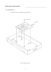
47 1) remove 4 screws ¶ and disassemble the loader ·. 5-1-5 loader removal disassembly and reassembly ¶ 4 screws · loader fig 5-5 loader removal.
Page 48
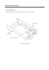
48 1) remove 7 screws ¶ and disassemble the front pcb ¸ from the front ass’y ·. ` 5-1-6 front pcb removal ¶ 7 screws · front ass’y ¸ front pcb disassembly and reassembly fig 5-6 front pcb removal.
Page 49: 6. Troubleshooting
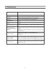
49 trouble action no power insert the ac power plug securely into the power outlet. No picture make sure that the equipment is connected properly. Make sure that the input setting for the tv is video (av). No sound make sure that the equipment is connected properly. Distorted sound make sure that th...
Page 50: Remained to Be Defined
50 troubleshooting remained to be defined.
Page 51: 7. Electrical Part List
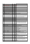
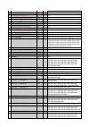
51 1.Main board 5.1 channel single scart location no spec pak' usa' no ass'y main 1 smps manual 1 2 hard disc cable, 25mm, 40pin 1 3 dvd loader, mechanism ass'y ass'y 1 pcb ass'y, main (t/u) 1 80c52(80c51), 40pin dip, mpu dip 1 u701 2 program memory 512k * 8 dip 1 u202 pcb ass'y, main (m/i) 1 power ...
Page 52
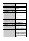
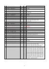
52 1 pcb, 2 layer fr4 1 2 cpu&risc single chip pqfp 1 u201 3 video encoder, ntsc/pal lqfp 1 u401 4 16m-sdram, 3.3v,400mil,512k*16*2 tsop(ii ) 2 u204,u203 5 ttl, hex inverter(fast) soic 1 u206 6 ttl, hex inverter soic 1 u207 7 eeprom, 2kbit,soic soic 1 u205 8 streo dac,192khz,24bit,20pin soic 1 u301 ...
Page 53
53 35 chip res', 1/10w,3.3k Ωj 1608 27 r201,r334,r342,r345,r347,r361,r405,r520,r525, r530,r535,r540,r545,r550,r555,r618,r619,r703, r705,r706,r707,r708,r709,r710,r713,r714,r717 36 chip res', 1/10w,47 Ωj 1608 9 r211,r212,r213,r214,r215,r216,r217,r218,r508 37 chip res', 1/10w,470 Ωj 1608 1 r404 38 chip...
Page 54
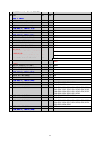
54 5.1 channel dual scart location no spec pak' usa' no ass'y main 1 smps manual 1 2 hard disc cable, 25mm, 40pin 1 3 dvd loader, mechanism ass'y ass'y 1 pcb ass'y, main (t/u) 1 80c52(80c51), 40pin dip, mpu dip 1 u701 2 program memory 512k * 8 dip 1 u202 pcb ass'y, main (m/i) 1 power con', 12pin, 2....
Page 55
55 1 pcb, 2 layer fr4 1 2 cpu&risc single chip pqfp 1 u201 3 video encoder, ntsc/pal lqfp 1 u401 4 16m-sdram, 3.3v,400mil,512k*16*2 tsop(ii) 2 u204,u203 5 ttl, hex inverter(fast) soic 1 u206 6 ttl, hex inverter soic 1 u207 7 eeprom, 2kbit,soic soic 1 u205 8 streo dac,192khz,24bit,20pin soic 1 u301 9...
Page 56
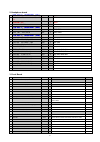
56 36 chip res', 1/10w,47 Ωj 1608 9 r211,r212,r213,r214,r215,r216,r217,r218,r508 37 chip res', 1/10w,470 Ωj 1608 1 r404 38 chip res', 1/10w,47k Ωj 1608 2 r239,r240 39 chip res', 1/10w,4.7k Ωj 1608 11 r101,r102,r204,r241,r242,r243,r510,r511,r513,r515 ,r517 40 chip res', 1/10w,5.6k Ωj 1608 12 r322,r32...
Page 57
57 2. Headphone board pcb ass'y, headphone (m/i) 1 headphone wire, 9pin-9pin(pcb), pcb in wire 1 con901 2 headphone jack 1 jac901 3 variable resistor 1 vr901 pcb ass'y, headphone (rad) 1 elec' cap', 22uf/16v,m 5mm 2 ce902,ce901 2 elec' cap', 47uf/25v,m 5mm 2 ce903,ce904 pcb ass'y, headphone (smd) 1 ...
Page 58
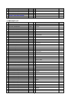
58 9 axi' res', 1/8w,56k Ωj axial 1 r12 10 axi' res', 1/6w,10k Ωj axial 6 r3,r4,r5,r6,r7,r8 11 axi' res', 1/6w,330 Ωj axial 1 r1 12 axi' res', 1/6w,22 Ωj axial 1 nr1 pcb ass'y, front bottum (smd) 1 vfd driver pqfp 1 u1 4. Smps part list no spec pak' usa' no pcb ass'y, smps (rad) 1 elec' cap', 220uf/...
Page 59
59 16 res-rd', 1/4w,2k Ωj 3 pr10,13,29 17 res-rd', 1/8w,4.7k Ωj 1 pr36 18 res-rd', 1/8w,6.8k Ωj 1 pr41 19 res-rd', 1/4w,270k Ωj 2 pr2,28 no spec pak' usa' no 20 res-rn', 1/8w,2k Ωj f 3 pr23,31,37 21 res-rn', 1/8w,12k Ωj f 1 pr45 22 res-rn', 1/8w,6.8k Ωj f 1 pr34 23 res-mof', 2w,15 Ωj (mor) 2 pr44,46...
Page 60: Remained to Be Defined
60 electrical part list remained to be defined.
Page 61: 8. Block Diagram
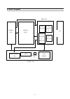
61 8. Block diagram power pcb loader (dvs) a/v decoder & main cpu vfd key matrix rcu remocon eye video encoder d/a converte r sub micom main pcb front pcb head phone pcb.
Page 62: Remained to Be Defined
62 block diagram remained to be defined.
Page 63: 9. Pcb Diagrams
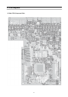
63 9. Pcb diagrams 9-1 main pcb (component side).
Page 64
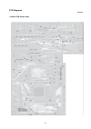
64 9-2 main pcb (solder side) pcb diagrams.
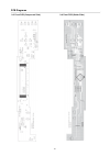
Page 65
65 9-3 front pcb (component side) 9-4 front pcb (solder side) pcb diagrams.
Page 66
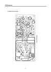
66 9-5 smps pcb (top side) pcb diagrams.
Page 67
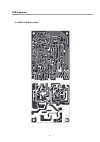
67 9-6 smps pcb (bottom side) pcb diagrams.
Page 68: 10. Wiring Diagram
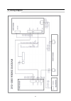
68 10. Wiring diagram.
Page 69: Remained to Be Defined
69 wiring diagram remained to be defined.
Page 70: 11. Schematic Diagrams
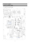
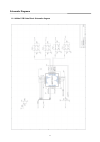
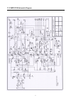
70 11. Schematic diagrams 11-1 main pcb schematic diagram 11-1-1 main pcb top schematic diagram.
Page 71
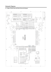
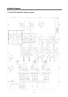
71 schematic diagrams 11-1-2 main pcb a/v decoder block schematic diagram.
Page 72
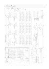
72 schematic diagrams 11-1-3 main pcb submicom block schematic diagram.
Page 73
73 schematic diagrams 11-1-4 main pcb video block schematic diagram.
Page 74
74 schematic diagrams 11-1-5 main pcb audio block schematic diagram.
Page 75
75 11-1-6 main pcb out stage block schematic diagram schematic diagrams.
Page 76
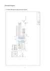
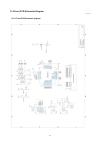
76 11-2 front pcb schematic diagram 11-2-1 front pcb schematic diagram.
Page 77
77 11-3 smps pcb schematic diagram.
Page 78: Remained to Be Defined
78 schematic diagrams remained to be defined.
Page 79
79 taeyoung telstar co.,ltd may.2001 printed in korea.

