- DL manuals
- Daewoo
- Receiver
- DR-C912B
- Service Manual
Daewoo DR-C912B Service Manual - Description of The Mechanism
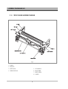
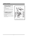
1.1 Characteristic of T6-DECK MECHANISM
1) T6-MECHA follows the VHS and the NTSC standard.
2) T6-MECHA uses 3 MOTORS (DRUM MOTOR, CAPSTAN MOTOR, L/C MOTOR).
3) T6-MECHA uses L/C Motor to drive FRONT LOADING.
4) T6-MECHA uses 4-BIT MODE signal to recognize each MODE.
This 4-BIT MODE signal is generated from the cam switch driven by the L/C MOTOR.
5) T6-MECHA has 7MODES (EJECT/INITIAL/REV/IDLE/PLAY,STOP,SLOW/BRAKE/FF&REW) operation.
6) T6-MECHA deduce the MODE changing time by adopting the full loading system which maintains the tape winding the
drum circumference.
7) T6-MECHA can be separated from the main pcb, and be assembled with B-B type connector. This B-B type connectioning
means that CAPSTAN MOTOR, LC MOTOR, AC HEAD, FE HEAD, DRUM are connected directly without using connector
cable.
12
DESCRIPTION OF THE MECHANISM
Summary of DR-C912B
Page 1
S/m no. : vcr9adpen0 ✔ caution : in this manual, some parts can be changed for improving, their perfor- mance without notice in the parts list. So, if you need the latest parts information,please refer to ppl(parts price list) in service information center (http://svc.Dwe.Co.Kr). Daewoo electronics ...
Page 2: Contents
Contents page number specifications .....................................................................1 cleaning and lubrication...........................................1 test equipment requirements ...................................2 the service fixture ..........................................
Page 3: Specifications
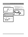
1 specifications cleaning and lubrication a. Cleaning the tape transport system the following parts should be cleaned after every 500 hours of use. • tension pole • s-guide post • fe head • s guide roller • s-slant pole • video head/drum • t-slant pole • t-guide roller • ac head/ae head • t-guide po...
Page 4
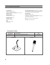
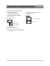
2 test equipment requirements fixture item description p/n path adj fixture use for x-position adjust/tape path alignment 97pb396000 special driver use for x-position adjust/tape path alignment the service fixture path adj fixture special driver 2 ac millivolt meter sensitivity: 1.0mvac–400vac dual-...
Page 5
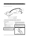
3 path fixture connection/test point identification 1. Preparation for replacement a. Soldering iron use a pencil-type soldering iron that uses less than 30 watts. B. Solder eutectic solder (tin 63%, lead 37%) is recommended. C. Soldering time do not apply heat more than 4 seconds. D. Preheating lea...
Page 6
4 path fixture connection/test point identification 3. Installing the leadless (chip) component 1) presolder the contact points of the circuit board. 2) press the part downward with tweezers and solder both electrodes as shown below. 4. Removing of flat ics(recommended procedure) 1) for removing sol...
Page 7
5 leadless (chip) component identification 1. Check the followings before s.M.D troubleshooting • cracked or chipped component body • cracked or separated solder joints • peeling end terminations or fractured leads 2. S. M. D (surface mounted devices) identification 1) chip resistor identification *...
Page 8: Abbreviations
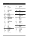
6 abbreviations a a or aud : audio a.E. : audio erase ac : alternating current acc : automatic color control acs : auto clock set afc : automatic frequency control aft : automatic fine tuning agc : automatic gain control alc : automatic level control am : amplitude modulation amp : amplifier ant : a...
Page 9
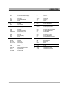
7 abbreviations pic : picture pif : picture intermediate frequency pll : phase locked loop ps : phase shift pwm : pulse width modulator pwr : power q q : transistor qv : quasi vertical r r : resistor, right rec : recording ref : reference reg : regulated, regulator remocon : remote control (unit) re...
Page 10: Instrument Disassembly
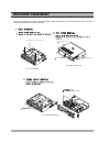
8 instrument disassembly fig. 1 - legs removal fig. 2 top cover removal perform all disassembly procedures in the order presented. When reassembling, use the reverse procedure. Make sure that all leads/wiring are routed correctly when reassembling. After releasing two screws, disassemble leg release...
Page 11
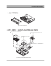
9 instrument disassembly fig. 5 . Deck & loader,power board removal after releasing seven screws, disassemble logic pcb 1 3 after releasing six screws, disassemble deck. After releasing four screws, disassem- ble loader. After releasing four screws, disassemble amp pcb. After releasing three screws,...
Page 12
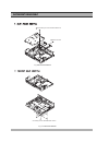
10 instrument disassembly fig. 6. Main board removal fig. 7. Chassis main removal release nine screws after releasing one screw, disassemble main pcb after releasing six screws, disassemble main chassis.
Page 13
11 instrument disassembly.
Page 14: Description of The Mechanism
1.1 characteristic of t6-deck mechanism 1) t6-mecha follows the vhs and the ntsc standard. 2) t6-mecha uses 3 motors (drum motor, capstan motor, l/c motor). 3) t6-mecha uses l/c motor to drive front loading. 4) t6-mecha uses 4-bit mode signal to recognize each mode. This 4-bit mode signal is generat...
Page 15
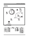
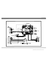
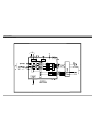
1.2 wire diagram 1.2.1 wire diagram 13 description of the mechanism 1.2.2 connector pin arrangement.
Page 16: Assembly Diagram and A/s
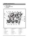
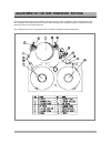
14 assembly diagram and a/s 2.1. Assembly diagram 2.1.1. Deck assembly diagram a. Upper view 1 mainbase ass y 2 drum ass y 3 fe head 4 s slant pole ass y 5 tension band ass y 6 s brake ass y 7 reel table 8 reel brkt total ass y 9 idler plate total ass y 10 t brake ass y 11 fl rack 12 relay lever 13 ...
Page 17
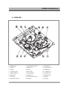
15 assembly diagram and a/s b. Lower view 1 mainbase ass y 2 drum ass y 3 fe head 4 s slant pole ass y 5 tension band ass y 6 s brake ass y 7 reel table 8 reel brkt total ass y 9 idler plate total ass y 10 t brake ass y 11 fl rack 12 relay lever 13 capstan motor 14 lc brkt ass y 15 pinch lever total...
Page 18
16 assembly diagram and a/s 2.1.2. Front loading assembly diagram 1 fl brkt l 2 top plate 3 safety lever 4 loading lever as4 5 cst holder as 6 door opener 7 safety lever r 8 fl brkt r fig.2.
Page 19
2.2 periodic maintenance and service schedule 2.2.1) periodic maintenance and service schedule a. In order to effectively maintain the excellent performance and fully utilize the features of this apperatus and to lengthen the life of mechanism and tapes, we strongly urge you to perform the periodic ...
Page 20
18 assembly diagram and a/s 2.3 jigs and tools 2.1 list of jigs and tools fig. No items model n o remarks ntsc: sp monoscope 7khz checking of the 1 alignment tape sp color bar 1khz ! Tape transporting (ep monoscope) section 2 cleaning tape dhc-602v @ checking of the tape (daewoo) transporting sectio...
Page 21
2..2 a skectch of jigs and tools 19 alignment tape ! # % & cleaning tape @ 30 20 10 0 10 20 30 30 20 10 0 10 20 30 vhs spindle height gauge $ ^ *.
Page 22
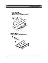
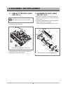
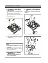
20 3. Disassembly and replacement 3.1 removal of the front loading assÕy (fig. 3.1) a. Unscrew the 2 screw holding the f/l. B. Separate the f/l ass‘y from the main base settling down point by lifting the rear part of f/l(screw hole). 3.2 disassembly of front loading assÕy(fig. 3.2~3.5) a. Remove the...
Page 23
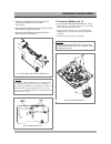
21 disassembly and replacement c. Separate the loading lever ass‘y by pressing the connection point from the cassette holder ass‘y.(fig. 3.3) d. Remove the safety spring connecting the safety lever and cassette holder plate.(fig. 3.3) e. Remove the release spring connecting the release lever and saf...
Page 24
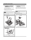
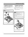
22 disassembly and replacement 3. 4. Disassembly of loading rack, loading assÕy, s/t slant pole assÕy(fig. 3.6, 3.7) a. Turn out the deck mechanism and remove the loading rack @ after unscrewing the screw . B. Disintegrate the r loading as # and l loading as $ . C. Disintegrate the s slant pole as %...
Page 25
23 disassembly and replacement 3. 6. Disassembly of the lc brkt assÕy, pinch lever total assÕy (fig. 3.9) a. Separate the lc brkt ass y @ after removing the 3 screws !. B. Separate the lc brkt ass y @ from the deck mechanism. C. Disintegrate the pinch lever total ass y #. 3. 7. Disassembly of the ca...
Page 26
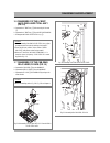
24 disassembly and replacement 3. 8 disassembly of the s/t brake assÕy(fig. 3.12) a. Unhook the s brake spring # from the mainbase hook !. B. Remove the s brake ass y @ from the mainbase. C. Remove the t brake spring ^ from the mainbase hook $. D. Remove the t brake ass y %. 3. 9 disassembly of the ...
Page 27
25 disassembly and replacement 3.12 disassembly of the reel table, idler plate total assÕy (fig. 3.15) a. Remove the poly washer ! And separate the idler plate total ass y @ from the mainbase. B. Remove the reel table $ from the reel table post # of the mainbase. 3.13 disassembly of the reel brkt to...
Page 28: Mechanical Adjustment
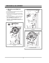
26 mechanical adjustment 4. 1 mechanical adjustment (fig. 4.1~4.4) in case of diassembly and reassembly for fixng the mecanical prob- lem, check the following check point. A. Make sure that the datum hole of the cam gear is aligned wth the datum hole in the mainbase in the eject modew as shown in fi...
Page 29
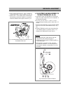
27 mechanical adjustment d. Make sure that the triangular mark a of the l loading ass y is aligned with the mark b of the r loading ass y. (fig. 4.4) e. Reference hole c of the loading rack should be aligned with the reference hole of the r loading ass y to make the teeth of the loading rack is alig...
Page 30
28 mechanical adjustment 4. 3 mechanical mode (operate with- out a cassette tape) a. Remove the front loading mechanism from the deck mechanism b. Cap the ir led and pull the fl rack. This has the same effect with cassette loading to the deck. C. If the s,t pole base is loaded, play mode starts auto...
Page 31
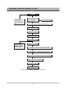
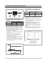
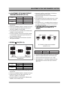
Generally, tape transporting section has been precisely adjusted in the factory and does not require the ordinary readjustment. But there is the case that tape noise or impact on the deck mechanism, tape transporting section readjustment is required. In adjustment of the tape transmission section co...
Page 32
30 adjustment of the tape transport section s/t guide roller height adjustment • drum total as • a/c head as • pinch lever total as s/t guide roller flunge a/c head as adjustment (tilt adjustment) cleaning audio azimuth adjustment a/c head adjustment x-position adjustment playback phase adjustment l...
Page 33
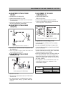
31 adjustment of the tape transport section a. Adjustment of the s/t guide roller a. Adjustment of the s/t guide roller a. Check the playing back with a t-120 tape. B. Make sure that excessive tape wrinkle does not occure ateatch s, t guide roller. C. If tape wrinkle is observed at the s/t guide rol...
Page 34
F. Playback phase adjustment(fig. 5.6) phase generator(pg) shifter determine the video head switching point when the tape is played back. If an adjust- ment of the phase generator(pg) shifter is not done pre- cisely, there can be a head switching noise or a verti- cal jitter problem, vibration of th...
Page 35
33 adjustment of the tape transport section h. Adjustment of the wave form of drum entrance /exit (fig. 5.8) a. Connect the pt01 on the main circuit board with a path adj.Fixture. B. Play back an alignment tape(dn-2 : monoscope signal) c. Connect the s/w pulse test pin on the path adj. Fix- ture wit...
Page 36
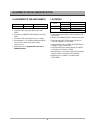
34 adjustment of the tape transport section k. Adjustment of the audio azimuth a. Connect the audio output jack with an audio level meter. B. Play back the alignment tape(dn-2:monoscope 7khz signal). C. Check if the audio output signal level is over : -9 ~-3dbm. D. If the requirement of c is not sat...
Page 37: Exploded View
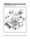
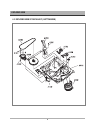
35 exploded view 6.1 exploded view of deck assÕy ( top view).
Page 38
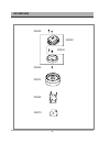
36 exploded view 6. 2 exploded view of deck assÕy ( bottom view).
Page 39
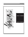
37 exploded view 6.3 exploded view of fl assÕy.
Page 40
38 exploded view d0040 d0040 d0020 d0050 d0010 d0060 d0070
Page 41
39 exploded view remark part name n o q’ty part no. Material.
Page 42: Electrical Adjustment
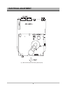
40 electrical adjustment fig. 1 main board test point/control location guide(component).
Page 43
41 electrical adjustment pg (pulse generator) shifter adjustment (fig. 3) test points: pt01 pin # main video out jack rear panel adjust: rec switch main the pulse generator (pg) shifter determines the video head switching point during playback. Misadjustment of the pg shifter may cause head switchin...
Page 44: Waveforms
42 waveforms video waveforms 480 4 6 20 34.
Page 45
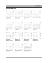
43 waveforms audio waveforms audio(normal) audio(hi-fi) ( (ic301-76) 150mvp-p 20mv/0.5msec/cm rec ) (ic301-10) 1.5vp-p 0.5v/0.5msec/cm rec 1 (ic301-9) 2.3vp-p 0.5v/0.5msec/cm rec 2 (ic301-2) 120mvp-p 50mv/0.5msec/cm play 3 (p201-2) 75vp-p 10v/20 µ sec/cm rec 4 (ic251-10) 80mvp-p 20mv/0.5msec ee/rec/...
Page 46
44 waveforms 24 25 26 27 31 30 29 28 servo waveforms.
Page 47
45 waveforms amp audio waveforms amp micom(ic220) pin#20(amp clk) amp micom(ic220) pin#21(amp clk) mclk ddx-8000 (ic200) pin#20 bck ddx-8000(ic200) pin#11 lrck ddx-8000 (ic200) pin#10 pcm0(downmix) ddx-8000 (ic200) pin#6 pcm1(front l/r) ddx-8000 (ic200) pin#9 pcm2(cen/sub) ddx-8000 (ic200) pin#7 pcm...
Page 48: Voltage Chart
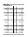
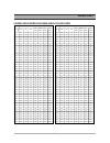
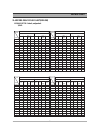
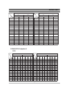
46 voltage chart 1 4.2 4.2 4.2 4.2 4.2 4.2 4.2 2 4.5 4.5 4.5 4.5 4.5 4.5 4.5 3 4.5 4.5 4.5 4.5 4.5 4.5 4.5 4 4.0 4.0 4.0 4.0 4.0 4.0 4.0 5 0 0 0 0 0 0 0 6 5.1 5.1 5.1 5.1 5.1 5.1 5.1 7 0 0 0 0 0 0 0 8 2 2 2 2 2 2 2 9 4.3 4.3 4.3 4.3 0.1 4.3 0.1 10 1.2 1.2 3 1.2 2.5 1.2 2 11 0 0 0 0 0 0 0 12 0 0 0 0 ...
Page 49
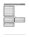
47 voltage chart 87 3.9 2.5 2.5 2.5 2.5 3.8 3.9 88 0 0 0 0 0 0 0 89 0 0 0 0 0 0 0 90 1.4 1.4 1.4 1.4 1.4 1.4 1.4 91 2.6 2.6 2.6 2.6 2.6 2.6 2.6 92 2.6 2.6 2.6 2.6 2.6 2.6 2.6 93 0 0 0 0 0 0 0 94 2.5 2.2 2.5 2.5 2.5 2.5 2.5 95 2.5 2.8 2.5 2.5 2.5 2.5 2.5 96 2.6 2.6 2.6 2.6 2.6 2.6 2.6 97 2.6 2.6 2.6 ...
Page 50
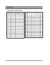
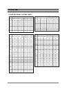
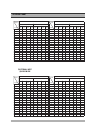
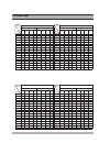
48 voltage chart 3. Ic driver/switch voltage charts 1 5.1 5.1 5.1 5.1 5.1 5.1 5.1 2 0 5.1 0 0 0 5.1 0 3 0 0 5 5 5 0 5 4 5 5 5 5 5 5 5 5 2.3 2.3 2.3 2.3 2.3 2.3 2.3 6 4.9 4.9 4.9 4.9 4.9 4.9 4.9 7 4.9 4.9 4.9 4.9 4.9 4.9 4.9 8 4.9 4.9 4.9 4.9 4.9 4.9 4.9 9 5 5 5 5 5 5 5 10 0 0 0 0 0 0 0 11 0 0 0 0 0 ...
Page 51
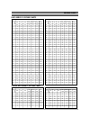
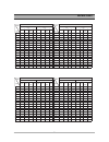
49 voltage chart 4. Video(luma/chroma) and linear audio voltage charts 1 2.4 2.4 2.4 2.4 2.4 2.4 2.4 2 2.4 3.0 2.4 2.4 2.4 2.4 2.4 3 2.4 2.4 2.4 2.4 2.4 2.4 2.4 4 2.4 2.4 2.4 2.4 2.4 2.4 2.4 5 2.4 2.4 2.4 2.4 2.4 2.4 2.4 6 2.4 2.4 2.4 2.4 2.4 2.4 2.4 7 0.0 1.7 0.0 0.0 0.0 0.0 0.0 8 2.4 2.3 2.4 2.4 2...
Page 52
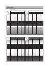
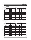
50 voltage chart 5. Video switching ic voltage charts 1 1.8 1.8 1.8 1.8 1.8 1.8 1.8 2 1.9 1.9 1.9 1.9 1.9 1.9 1.9 3 2 2 2 2 2 2 2 4 1.9 1.9 1.9 1.9 1.9 1.9 1.9 5 0 0 0 0 0 0 0 6 0 0 0 0 0 0 0 7 0 0 0 0 0 0 0 8 4.1 4.1 4.1 4.1 4.1 4.1 4.1 mode ic401 pin no. Stop rec play rew/ rev/fwd rec play f.Fwd s...
Page 53
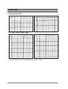
51 voltage chart 6. Hifi audio ic voltage charts 1 2.5 2.5 2.5 2.5 2.5 2.5 2.5 2 0 0 0 0 0 0 0 3 2.5 2.5 2.5 2.5 2.5 2.5 2.5 4 0 0 0 0 0 0 0 5 2.2 2.2 2.2 2.2 2.2 2.2 2.2 6 2.5 2.5 2.5 2.5 2.5 2.5 2.5 7 2 2 2 2 2 2 2 8 0.3 0.3 0.3 0.3 0.3 0.3 0.3 9 0 0 0 0 0 0 0 10 0 0 0 0 0 0 0 11 0 0 0 0 0 0 0 12 ...
Page 54
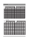
52 voltage chart * this can be measured in the only default and configuration 1 mode. 8. Tmi voltage chart 9 . Ic codec cs4228 voltage chart 1 0 0 0 0 0 0 0 2 0.4 0.4 0.4 0.4 0.4 0.4 0.4 3 5 5 5 5 5 5 5 4 5 5 5 5 5 5 5 5 1.4 1.4 1.3 1.5 1.3 1.5 1.3 6 0 0 0 0 0 0 0 7 0 0 0 0 0 0 0 8 0 0 0 0 0 0 0 mod...
Page 55
53 voltage chart 10. Amp mi-com voltage chart(w78e58bp-42) 1. Dvd mode 2. External input 1) vcr mode.
Page 56
54 voltage chart 2) am/fm mode *1 : it is changed according to the state of am/fm. *2 : it is changed according to the option resistances(r205, r206, r207, r208, r209). - existing option resistances : 0v - no existing option resistances : 5.2v.
Page 57
55 voltage chart 11. Amp ddx-8000 voltage chart(ddx-8000) 1. Speaker setup : default, configuration1 1) dvd mode pinno. Ic ddx-8000(ic200) mode pinno. Ic ddx-8000(ic200) 2ch 5.1ch 2ch 5.1ch stop play play pause mute stop play play pause mute stop play play pause mute stop play play pause mute 1 0 0 ...
Page 58
56 voltage chart 1) external input (1) video mode mode pinno. Ic ddx-8000(ic200) mode pinno. Ic ddx-8000(ic200) 2ch 5.1ch 2ch 5.1ch stop play play pause mute stop play play pause mute stop play play pause mute stop play play pause mute 1 0 0 0 0 0 0 0 0 33 0 5.1 0 0 0 5.1 0 0 2 0 0 0 0 0 0 0 0 34 0 ...
Page 59
57 voltage chart (2) am/fm mode mode pinno. Ic ddx-8000(ic200) mode pinno. Ic ddx-8000(ic200) 2ch 5.1ch 2ch 5.1ch am fm am fm am fm am fm 1 0 0 0 0 33 5.1 5.1 5.1 5.1 2 0 0 0 0 34 5.1 5.1 5.1 5.1 3 3.3 3.3 3.3 3.3 35 3.3 3.3 3.3 3.3 4 0 0 0 0 36 0 0 0 0 5 2.5 2.5 2.5 2.5 37 2.5 2.5 2.5 2.5 6 3.3 3.3...
Page 60
58 voltage chart 2. Speaker setup : configuration 2 , 3 1) dvd mode pinno. Ic ddx-8000(ic200) mode pinno. Ic ddx-8000(ic200) 2ch 5.1ch 2ch 5.1ch stop play play pause mute stop play play pause mute stop play play pause mute stop play play pause mute 1 0 0 0 0 0 0 0 0 33 0 0 0 0 0 0 0 0 2 0 0 0 0 0 0 ...
Page 61
59 voltage chart 2) external input (1) video mode mode pinno. Ic ddx-8000(ic200) mode pinno. Ic ddx-8000(ic200) 2ch 5.1ch 2ch 5.1ch stop play play pause mute stop play play pause mute stop play play pause mute stop play play pause mute 1 0 0 0 0 0 0 0 0 33 0 0 0 0 0 0 0 0 2 0 0 0 0 0 0 0 0 34 0 0 0 ...
Page 62
60 voltage chart (2) am/fm mode mode pinno. Ic ddx-8000(ic200) mode pinno. Ic ddx-8000(ic200) 2ch 5.1ch 2ch 5.1ch am fm am fm am fm am fm 1 0 0 0 0 33 5.1 0 5.1 0 2 0 0 0 0 34 5.1 0 5.1 0 3 3.3 3.3 3.3 3.3 35 3.3 3.3 3.3 3.3 4 0 0 0 0 36 0 0 0 0 5 2.5 2.5 2.5 2.5 37 2.5 2.5 2.5 2.5 6 3.3 3.3 3.3 3.3...
Page 63
61 voltage chart mode pinno. Ddx-2100(ic301) mode pinno. Ddx-2100(ic301) 2ch 5.1ch 2ch 5.1ch stop play play pause mute stop play play pause mute stop play play pause mute stop play play pause mute 1 0 0 0 0 0 0 0 0 19 0 0 0 0 0 0 0 0 2 0 0 0 0 0 32.5 0 0 20 0 0 0 0 0 0 0 0 3 0 0 0 0 0 32.5 0 0 21 4....
Page 64
62 voltage chart mode pinno. Ddx-2100(ic360) mode pinno. Ddx-2100(ic360) 2ch 5.1ch 2ch 5.1ch stop play play pause mute stop play play pause mute stop play play pause mute stop play play pause mute 1 0 0 0 0 0 0 0 0 19 0 0 0 0 0 0 0 0 2 0 32.5 0 0 0 32.5 0 0 20 0 0 0 0 0 0 0 0 3 0 32.5 0 0 0 32.5 0 0...
Page 65
63 voltage chart mode pinno. Ddx-2100(ic330) mode pinno. Ddx-2100(ic330) 2ch 5.1ch 2ch 5.1ch stop play play pause mute stop play play pause mute stop play play pause mute stop play play pause mute 1 0 0 0 0 0 0 0 0 19 0 0 0 0 0 0 0 0 2 0 32.5 0 0 0 32.5 0 0 20 0 0 0 0 0 0 0 0 3 0 32.5 0 0 32.5 32.5 ...
Page 66
64 voltage chart (2) am/fm mode mode pinno. Ic ddx-2100(ic301) mode pinno. Ic ddx-2100(ic301) 2ch 5.1ch 2ch 5.1ch am fm a m fm am f m am fm 1 0 0 0 0 19 0 0 0 0 2 32.5 0 32.5 32.5 20 0 0 0 0 3 32.5 0 32.5 32.5 21 4.8 4.8 4.8 4.8 4 32.5 32.5 32.5 32.5 22 4.8 4.8 4.8 4.8 5 0 0 0 0 23 3.3 3.3 3.3 3.3 6...
Page 67
65 voltage chart mode pinno. Ic ddx-2100(ic360) mode pinno. Ic ddx-2100(ic360) 2ch 5.1ch 2ch 5.1ch am fm a m fm am f m am fm 1 0 0 0 0 19 0 0 0 0 2 32.5 32.5 32.5 32.5 20 0 0 0 0 3 32.5 32.5 32.5 32.5 21 4.8 4.8 4.8 4.8 4 32.5 32.5 32.5 32.5 22 4.8 4.8 4.8 4.8 5 0 0 0 0 23 3.3 3.3 3.3 3.3 6 0 0 0 0 ...
Page 68
66 voltage chart mode pinno. Ddx-2100(ic330) mode pinno. Ddx-2100(ic330) 2ch 5.1ch 2ch 5.1ch stop play play pause mute stop play play pause mute stop play play pause mute stop play play pause mute 1 0 0 0 0 0 0 0 0 19 0 0 0 0 0 0 0 0 2 0 32.5 0 0 0 32.5 0 0 20 0 0 0 0 0 0 0 0 3 0 32.5 0 0 0 32.5 0 0...
Page 69
67 voltage chart 2) external input (1) video mode mode pinno. Ddx-2100(ic301) mode pinno. Ddx-2100(ic301) 2ch 5.1ch 2ch 5.1ch stop play play pause mute stop play play pause mute stop play play pause mute stop play play pause mute 1 0 0 0 0 0 0 0 0 19 0 0 0 0 0 0 0 0 2 0 0 0 0 0 32.5 0 0 20 0 0 0 0 0...
Page 70
68 voltage chart mode pinno. Ddx-2100(ic360) mode pinno. Ddx-2100(ic360) 2ch 5.1ch 2ch 5.1ch stop play play pause mute stop play play pause mute stop play play pause mute stop play play pause mute 1 0 0 0 0 0 0 0 0 19 0 0 0 0 0 0 0 0 2 0 0 0 0 0 0 0 0 20 0 0 0 0 0 0 0 0 3 0 0 0 0 0 0 0 0 21 4.8 4.8 ...
Page 71
69 voltage chart mode pin no. Icddx-2100(ic330) mode pinno. Ic ddx-2100(ic330) 2ch 5.1ch 2ch 5.1ch a m fm a m fm am fm a m fm 1 0 0 0 0 19 0 0 0 0 2 32.5 32.5 32.5 32.5 20 0 0 0 0 3 32.5 32.5 32.5 32.5 21 4.8 4.8 4.8 4.8 4 32.5 32.5 32.5 32.5 22 4.8 4.8 4.8 4.8 5 0 0 0 0 23 3.3 3.3 3.3 3.3 6 0 0 0 0...
Page 72
70 voltage chart ic smps/fet/photo coupler/regulator/tr voltage charts 1 nc nc nc nc nc nc 2 6 5.6 5.6 5.6 5.6 5.6 3 1.5 2.1 2.3 2.2 2.4 2.1 4 8.6mv 37mv 50mv 42mv 59mv 38mv mode smps controller(ic801) [v] pin no. Off pwr on dvd play dvdoff dvd play fm/am & vcr off vcr play &vcr rec 5 1.55 2.6 2.89 ...
Page 73
71 voltage chart 1 6.9 6.3 6.2 6.3 6.2 6.3 2 0 5 5 5 5 5 3 0 0 0 0 0 0 4 0.6 5.1 5.1 5.1 5.1 5.1 mode ic regulator(ic902) [v] pin no. Off pwr on dvd play dvdoff dvd play fm/am & vcr off vcr play &vcr rec d 4.4 3.5 3.4 3.5 3.5 3.4 g 0 13.4 12.7 13.1 12.6 13.3 s 0.2 3.4 3.4 3.4 3.4 3.4 mode fet(q903)[...
Page 74: Troubleshooting
72 troubleshooting power circuit check ic601, ic701. No power power cord is ok? Is 120~200v voltage obtained at c801+? Output voltage of 2 nd parts is abnormal? Check rectifier diode of 2 nd parts ; d901,d903,d904,d905,d906, d907,d908,d909,r921. Switching pulse of q801 drain, q701 drain is normal? O...
Page 75
73 troubleshooting system circuit no vfd display. Is 5v obtained at ic701 pin#13? Is -24v obtained at ic701 pin#30? Oscillation at ic701 pin #8? Is -24v, -20v obtained at f-, f+? Specific grid/seg doesn’t function. Check d721. Check power circuit at -24v. Check ic701. Check ic 701 pin #31~42. Check ...
Page 76
74 troubleshooting no power compensation. Voltage of power fail (ic601 pin#100) at micom is 0.7v over? More than 3.2v is maintained for 1 minutes at ic601 pin#37 during power cord open. Check r625. No yes b. No power compensation. Yes check reset circuit. No exchange ic601. Noise appears on the play...
Page 77
75 troubleshooting noise appears on the full playback screen. Are sw pulse and ha sw normal? Recheck step c-1 (bad playback quallty (1)). Check head amp connector and head. Yes yes no no enve wave at pt01 pin #4? Check video circuit. Are there sw, ha sw pulse at ic601 pin #16, 18? Check pcb pattern....
Page 78
76 troubleshooting cassette tape isn’t inserted. Is 5v voltage obtained at loading parts ic601 pin#82? Is 13v voltage obtained at capstan motor pin#8? Check at power circuit 14v. Check (d905, d906). Connect capstan and loading motor. Check connector and capstan motor. Yes no no no is 12v voltage obt...
Page 79
77 troubleshooting g. Drum motor stops h. Capstan doesn’t rotate capstan doesn’t rotate. Is 14v voltage obtained at p603 pin#2? Yes no no no yes yes is capstan pwm fit to ic 601 pin#77? Is 3.2v voltage obtained at p603 pin#5? Is 2~3v voltage obtained at p603 pin#9? Check p603 connector and capstan m...
Page 80
78 troubleshooting a. Ee screen doesn’t appear ee screen doesn’t appear. Is video signal input at ic301 pin#28, 30, 32? Is 5v obtained at ic301 pin#23, 44, 45, 52, 68? Is c.S, data, clock signal input ic301 pin#53,54,55? Is video signal output at ic601 pin#52? Check ic401, line jack and if circuit. ...
Page 81
79 troubleshooting b. Playback picture doesn’t appear yes yes is y signal output at ic301 pin#35? Is y signal input at ic301 pin#39? Check and replace ic301. Playback picture doesn’t appear. Is c.S, data, clock signal input ic301 pin#53,54,55? No no yes check ee mode and osd circuit check ic pin#61,...
Page 82
80 troubleshooting is 5v obtained at ic301 pin#68? No no yes yes is video sw pulse input at ic301 pin#57? Is rec signal input at ic301 pin#66,73? Ep mode: pin #73 sp mode: pin #66 check video head and connector. Is signal input at ic301 pin# 28, 30,32? Check power circuit. Check ic601 pin#18. No rec...
Page 83
81 troubleshooting no is power_on_h signal output at pj601 pin#11. Change video mode. No logo display. Do not open tray is video mode-s-video mode? Is power supplied cn2? (in dvd loader pcb) no e. No logo display or do not open tray.(dvd) yes yes check ic 601 pin#29 and pcb pattern. Is video signal ...
Page 84
82 troubleshooting 1. Rca a. No sound in e-e mode audio circuit no sound in rf e-e mode check output jack. A-1. Tv e-e no check ic601. Is audio signal output at ic251 pin#53, 57? Are clk and data obtained at ic251 pin#42,43? No is 5v obtained at ic251 pin#40? Is there sif signal at ic251 pin#48 in r...
Page 85
83 troubleshooting ic 12v obtained at ic252 pin #16? Yes check output jack. Yes no check ic601. No sound in line1 e-e mode. Is 12v obtained at ic251 pin#58? No is 5v obtained at ic251 pin#40? Check power circuit. Yes no are clk and data obtained at ic251 pin#42,43? Check input line1 jack replace ic2...
Page 86
84 troubleshooting ic 12v obtained at ic252 pin #16? Yes check output jack. Yes no check ic601. No sound in line2 e-e mode. Is 12v obtained at ic251 pin#58? No is 5v obtained at ic251 pin#40? Check power circuit. Yes yes no are clk and data obtained at ic251 pin#42,43? Check input line2 jack replace...
Page 87
85 troubleshooting ic 12v obtained at ic252 pin #16? Yes check output jack. Yes no check ic601. No sound in line3(front) e-e mode. Is 12v obtained at ic251 pin#58? No is 5v obtained at ic251 pin#40? Check power circuit. Yes no are clk and data obtained at ic251 pin#42,43? Check input line3 jack repl...
Page 88
86 troubleshooting a-5. Dvd e-e is there reset at icd01 #14? No no yes yes is 12v obtained at icd02 #8? Are there signal at icd02 #1, #7? Is 12v obtained at ic251 #58? Check dvd board. Check signal flow circuit. No sound dvd ee mode. Are there voltage at icd01 #8(5v), #9(3.3v), #21(5v)? Yes are ther...
Page 89
87 troubleshooting a-6. Subwoofer pre-out e-e are there clocks at icd01 #5(bclk), #6(lrclk), #10(mclk)? No no yes yes is there reset(h) at icd01 #14? Is 12v obtained at icd03 #8? Are there signals at icd03 #1? Check power circuit. Check dvd board. No sound subwoofer pre- out ee mode. Is speaker setu...
Page 90
88 troubleshooting is there playback audio signal at ic251 pin#53, 57? Are clk and data obtained at ic251 pin#42, 43? No is theremute(h) at ic251 pin#36? Check ic601. Yes is a.Sw signal input at ic251 pin #27? Check drum connector and drum. No check a.Sw at ic601 pin#19. No replace ic251. Yes no is ...
Page 91
89 troubleshooting are there audio signal at ic251 pin#9,14 #10, 15 #2,4? Is there rec(h) at ic251 pin#29, 30? Check input line1 jack. Check input line2 jack. Check input line3(front) jack. Replace ic251 yes no no no is fm osc signal at ic251 pin#21? Is fm osc signal at p301 pin#2? Check ic601 pin#2...
Page 92
90 troubleshooting d. No normal audio playback (play mode) is playback audio signal at ic301 pin#10? Replace ic251. Yes no no is there playback normal audio signal at ic251 pin#53,57? Check a/c head and ic301 yes check output jack. Yes is there normal audio signal at ic251 pin#53, 57? No check power...
Page 93
91 troubleshooting e. No normal audio playback in record/playback mode(check in rec mode) no normal audio playback in record/playback mode are there audio signal at ic251 pin#9,14 #10,15 #2,4? Is there recording signal at ic251 pin#61? Check input line1 jack. Check input line2 jack. Check input line...
Page 94
92 troubleshooting 2. Headphone is there reset(h) at icd01 #14? No no yes yes is 12v obtained at icd03 #8? Are there signals at icd04 #1, #7? Check dvd board. Check signal flow circuit. No sound in dvd or external mode. Are there voltages at icd01 #8(5v), #9(3.3v), #21(5v)? Yes are there clocks at i...
Page 95
93 troubleshooting is+3.3v obtained at ic200 vdd_3.3? Is+2.5v obtained at ic200 vdd_2.5? Is+3.3v obtained at the ibias of ic301,ic330,ic360? Check power circuit. Yes yes yes no is+32.5v obtained at the vcc of ic301,ic330,ic360? Yes yes check ic220 no is there ‘h’ at ic200 #64(pwdn)? Is there ‘h’ out...
Page 96
94 troubleshooting is+5v obtained at ic220 #9, #35, #44? Is+3.3v obtained at ic200 vdd_3.3? Is+2.5v obtained at the ic220 vdd_2.5? Check power circuit. Yes yes yes no is there ‘l’ at ic220 #10? Yes yes check ic601 and data ports. No is there normal 12mhz oscillation signal at ic220 #20, #21? Check x...
Page 97
95 troubleshooting the protect takes place in the vfd are the #4,#7,#12,#17 of ic 301, ic330,ic360 connected to the ground? Are the #2~3, #8~9,#10~11,#16~17 of ic301,ic330,ic360 connected the ground? Is+4v obtained at #26(tri),#27(fault) of ic301,ic330,ic360? Check ic301, ic330,ic360 and replace inf...
Page 98
96 troubleshooting is +12v obtained at rf102 #3? When tunning play are there normal pll control signals at ic220 #3~#6? When tuned, is there ‘l’ at rf102 #1, #2? Check power circuit. Check rf102 and replace inferior device. Yes yes yes no no no when tuned, is there audio signals at rf102 #4, #6? Che...
Page 99
97 troubleshooting yes check power circuit. No are there voltage at icd01 #18(5v) #9(3.3v), #21(5v)? Check signal flow circuit. No are there normal audio signals at icd01 #16~#17, #19~20? Yes no sound in external(video) mode. Check dvd board. No are there clock at icd01#5(bclk), #6(lrclk), #10(mclk)...
Page 100
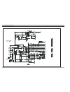
98 schematic diagram power supply schematic diagram 11 + c913 33uf 50v r713 0.22 1w(metal oxide) (open) d910 22 r809 -24v / 10ma 2 103 1kv c803 3 power det 390k r802 1.3kf r913 the parts identified by 8d-13 th801 1k(open) r909 cn902 6p 1 2 3 4 5 6 f.G. 6v / 1a uf4004 d912 1.8kf r912 1 13 l903 22uh(c...
Page 101
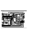
Servo & syscon schematic diagram (dvd combo receiver) 99 schematic diagram.
Page 102
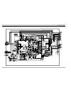
100 schematic diagram video/audio schematic diagram (dvd combo receiver).
Page 103
Hi-fi & s/w & pif & mpx schematic diagram (dvd combo receiver) 101 schematic diagram.
Page 104
Digital audio/video schematic diagram(dvd combo receiver) 102 schematic diagram.
Page 105
Receiver front part schematic diagram 103 schematic diagram.
Page 106
104 schematic diagram digital amp schematic diagram.
Page 107
Hdd6 hdd1 hdd15 hdd0 hdd3 hdd5 hdd10 hdd[0..15] hdd14 hdd11 hdd7 hdd2 hdd13 hdd8 hdd12 hdd4 hdd9 1 + 1 + 1 + 1 2 3 4 5 6 1 + + + 1 + + 1 105 schematic diagram dvd schematic diagram 1. Atapi i/f.
Page 108
Memory control signal n o te: l1 and c41 are populated on ly wh en a 3 rd o verto ne xtal is used at y1. 3 1 mmbt2 222a 2 5pin front panel connector mcko mcken casl rasl we l pcm_d0 pcm_ xc k pcm_lrck ma 1 ma 4 atapi_int n_wel hms_d8 pcm_d3 pcm_d1 md2 vid_d[0:7] reset_l vid_d5 ma 0 ma 3 md29 hms_rd_...
Page 109
107 schematic diagram dvd schematic diagram 3. Memory interface other 512k x 4 bank x 32 bit sdrams: micron: mt48lc2m32b1tg-8e samsung: km432s2030b-8 toshiba: tc59s6432cft-80 winbond: w986432ah-8 assebily note : for production : don't install j3, r26, j2, c13, c14 for engineering : don't install r25...
Page 110
7 bit i 2c addr ess = 50 scl i2c serial eep ro m 256 byte heat sink area for u2 : for the device, allow 12mm sq copper area on layer 1. That is connected to the "tab" (pin 4). Sd a master/slave i2c port for e-romulator heat sink area for u1 : for the device, allow 25mm sq copper area on layer 1. Tha...
Page 111
109 schematic diagram dvd schematic diagram 5. Video & audio.
Page 112
110 block diagram receiver servo & syscon block diagram.
Page 113
111 block diagram combo receiver video block diagram.
Page 114
Normal audio block diagram 112 block diagram.
Page 115
113 block diagram drc6000n, drc6000l hi-fi audio block diagram rev.0 2002.09.03 hi-fi & s/w & pif block diagram.
Page 116
114 block diagram digital audio block diagram.
Page 117
Amp block diagram 115 block diagram.
Page 118
Main pcb circuit board(rtd300) 116 circuit board index.
Page 119
117 circuit board index power/logic pcb circuit board(rtd300).
Page 120
118 circuit board index amp pcb circuit board(rtd300).
Page 121: Electrical Partslist
119 electrical partslist loc parts_code parts_name parts_description remark z800 97pd203300 pcb power manual as icr 300dn ac85~265v 300w 300 watt power z800 97pd205100 power module as icr 200dn ac85~265v 200w 200 watt power c101 cexf1a471v c electro 10v rss 470mf (8x11.5) tp main pcb c102 hcbk103kba...
Page 122
120 electrical partslist loc parts_code parts_name parts_description remark c311 hcbk104kba c chip cera 50v x7r 0.1mf k 1608 main pcb c312 cexf1c100a c electro 16v rsm 10mf 5x7 main pcb c313 cexf1c100a c electro 16v rsm 10mf 5x7 main pcb c314 cexf1h109a c electro 50v rsm 1mf (4x7) tp main pcb c315 c...
Page 123
121 electrical partslist loc parts_code parts_name parts_description remark cd30 cexf1c100a c electro 16v rsm 10mf 5x7 main pcb cd33 cexf1c220a c electro 16v rsm 22mf (5x7) main pcb cd34 hcqk100jba c chip cera 50v ch 10pf j 1608 main pcb cd37 hcqk100jba c chip cera 50v ch 10pf j 1608 main pcb cd38 c...
Page 124
122 electrical partslist loc parts_code parts_name parts_description remark l103 5cpx688k2t coil peaking 0.68uh(blu-silv) main pcb l104 5cpx101j2t coil peaking 100uh(brn-brn) main pcb l105 5cpx101j2t coil peaking 100uh(brn-brn) main pcb l106 85801060ta wire copper 0.6x52mm taping main pcb l107 85801...
Page 125
123 electrical partslist loc parts_code parts_name parts_description remark r205 hrfs273jba r chip 1/16 27k ohm j 1608 main pcb r206 hrfs821jba r chip 1/16 820 ohm j 1608 main pcb r207 hrfs333jba r chip 1/16 33k ohm j 1608 main pcb r208 rd-az622j- r carbon film 1/6 6.2k ohm j main pcb r212 hrfs822jb...
Page 126
124 electrical partslist loc parts_code parts_name parts_description remark r601 rd-az102j- r carbon film 1/6 1k ohm j main pcb r602 rd-az103j- r carbon film 1/6 10k ohm j main pcb r604 85801060ta wire copper 0.6x52mm taping main pcb r605 hrfs103jba r chip 1/16 10k ohm j 1608 main pcb r606 hrfs103jb...
Page 127
125 electrical partslist loc parts_code parts_name parts_description remark rd56 hrfs103jba r chip 1/16 10k ohm j 1608 main pcb rd58 hrfs181jba r chip 1/16 180 ohm j 1608 main pcb rd59 hrfs181jba r chip 1/16 180 ohm j 1608 main pcb rd63 hrfs512jba r chip 1/16 5.1k ohm j 1608 main pcb rd64 hrfs102jba...
Page 128
126 electrical partslist loc parts_code parts_name parts_description remark jp709 85801065gy wire copper awg22 1/0.65 tin coating front pcb jp710 85801065gy wire copper awg22 1/0.65 tin coating front pcb jp711 85801065gy wire copper awg22 1/0.65 tin coating front pcb jp712 85801065gy wire copper awg...
Page 129
127 electrical partslist loc parts_code parts_name parts_description remark c254 hcfh104zba c chip cera 25v y5v 0.1mf z 1608 amp pcb c255 hcfh104zba c chip cera 25v y5v 0.1mf z 1608 amp pcb c256 hcfh104zba c chip cera 25v y5v 0.1mf z 1608 amp pcb c257 hcfh104zba c chip cera 25v y5v 0.1mf z 1608 amp ...
Page 130
128 electrical partslist loc parts_code parts_name parts_description remark p200 97p62g08e7 conn ffc gf102-07s-ts 07p st amp pcb p201 97p62g08ev conn ffc gf102-29s-ts 29p st amp pcb p301 97p62g08eb conn ffc gf102-11s-ts 11p st amp pcb q201 tzrc104m tr krc104m auto amp pcb q202 tzrc104m tr krc104m au...
Page 131
129 electrical partslist loc parts_code parts_name parts_description remark sp01 48a83084a2 speaker system htwcfr-300ba2 300 watt sp01 48a83078a2 speaker system htwcfr-200ba2 200 watt m100 97qd020200 total dvd rl-s900(mecha+servo+mpeg) tce dvd m101 97pb253200 dvd door as 25901+09500 dr-c91d1n-bs dvd...
Page 132
686, ahyeon-dong mapo-gu seoul, korea c.P.O. Box 8003 seoul, korea daewoo electronics corp..


