- DL manuals
- Daewoo
- Receiver
- DSD-9251EAV
- Service Manual
Daewoo DSD-9251EAV Service Manual - General Information
2
GENERAL INFORMATION
Digital Satellite Receiver is easy to use, and allows you to watch digital programs broadcasted via satellite.
This instruction manual will guide you through the initial installation of your receiver.
It also describes how to take full advantage of a wide range of features that are easily accessible.
Read this instruction manual carefully before installing your receiver.
MAIN FEATURES
• High quality Digital Video & Audio
• Fully DVB compliant
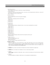
• Common Interface with 2 PCMCIA slots
• User friendly and easy-to use menu system
• Various channel editing function, on Channel Management. (favorite, move, lock, rename, delete and sort)
• User programmable Satellite & Transponder information
• Automatic search for newly added transponder (NIT search)
• Stores up to 4000 channels
• Support software upgrading through RS-232C port
• Plug-and-play data transfer system (DSR to DSR)
• Individual channel volume saving function
• Timer function
• Automatic reserved channel moving system
• Electronic Program Guide (EPG)
• Teletext function support
• Support RGB and CVBS video output
• SCPC/MCPC receivable from C/Ku Band
• Multi LNB control by DiSEqC 1.0 and 22 KHz switching
• Motorized system control by DiSEqC 1.2* and USALS**.
• 256 color On-Screen-Display
• Support S/PDIF output (Optional function)
* DiSEqC
TM
is a trademark of EUTELSAT.
** USALS
TM
is a trademark of Stab.
Summary of DSD-9251EAV
Page 1
S/m no. : dsd9251m01 ✔ caution : in this manual, some parts can be changed for improving, their performance without notice in the parts list. So, if you need the latest parts information,please refer to ppl(parts price list) in service information center (http://svc.Dwe.Co.Kr). Daewoo electronics co...
Page 2
General information............................................................................................2 circuit operation manual .............................................................................................7 fixing errors ........................................................
Page 3: General Information
2 general information digital satellite receiver is easy to use, and allows you to watch digital programs broadcasted via satellite. This instruction manual will guide you through the initial installation of your receiver. It also describes how to take full advantage of a wide range of features that...
Page 4
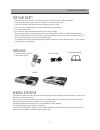
For your safety • allow clear space of more than 10 cm from the top, back and both sides for sufficient ventilation. • do not cover the digital satellite receiver nor place it on a unit that emits heat. • use a soft cloth and a mild solution of washing liquid to clean the casing • do not connect or ...
Page 5
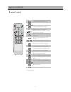
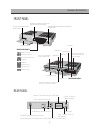
4 general information remote control switches between the operational mode and stand-by mode of the receiver switches between tv and av mode used for various functions on some menu displays the menu on the screen change channel, or moves to the next higher or lower item in the menu adjusts the volum...
Page 6
5 general information front panel rear panel 2 ci slot for conditional access module (cam) changes the channel or moves to the previous/next item in the menu switches between the operational mode and stand-by mode opened front door front panel display upload in process download in process error in d...
Page 7
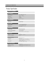
6 general information product specification transmission standards lnb/tuner input system resources video decoder audio decoder power supply rear panel interfaces remocon transmitter dvb, mpeg2 connector iec 169-24, female-type input frequency 950 ~ 2150mhz demodulation 2 msps ~ 35msps code rate qps...
Page 8
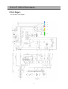
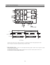
7 circuit operation manual 1. Block diagram dsd-9251eav block diagram.
Page 9
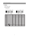
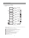
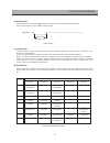
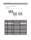
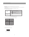
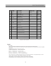
8 circuit operation manual 2. Interface (1) remote controller interface " power " custom code : e8 h data code : 15 h key no key name custom code(h) data code(h) custom code(b) data code(b) k01 1 e8 h 01 h 0001 0111 1000 0000 k02 2 e8 h 02 h 0001 0111 0100 0000 k03 3 e8 h 03 h 0001 0111 1100 0000 k0...
Page 10
9 circuit operating manual key function hex key function hex custom code 0xe8 pg down 0x1d 0 0x00 pg up 0x1c 1 0x01 3 0x14 2 0x02 4 0x13 3 0x03 menu 0x22 4 0x04 exit 0x23 5 0x05 tv/radio 0x0a 6 0x06 recall 0x20 7 0x07 info 0x21 8 0x08 epg 0x24 9 0x09 uhf 0x26 0x15 sat 0x10 tv/av 0x16 freeze 0x1e 0x1...
Page 11
10 circuit operation manual (1) structure sti5518 is a 1 chip including 32bit risc cpu, a/v demux, video encoder, multi pio and cache ram for the use o dvb and dss set top. Followings are summary of distinctive features of each block. Enhanced capability with 32bit vl-risc cpu core of 81mhz clock. S...
Page 12
11 circuit operation manual (2) reset section. If the low signal is read by sti5518 reset pin, the register value of all sti5518 will be initialized. There must be at least of 8 clock (37nsec) of reset time. (3) clock section. Sti5518 has two pll inside. Operative clocks are made by external clock w...
Page 13
12 circuit operation manual this section only provides summaries of individual function of each port. Further discussion will be followed in individual port section. I 2 c_data (pio1_0) i 2 c_clk (pio1_2) used for the transmission of serial and control of tuner, ci-max, av switch and rf modulator. C...
Page 14
13 circuit operation manual notpgm_en (pio1_3) flash rom write protect/ program enable (low) or program disable (high) slow_s/w (pio1_4) checking the connection of external features with vcr scart such as vcr and general power on/off status. Connect and power on(high), not connect or power off(low) ...
Page 15
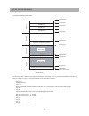
14 circuit operation manual following is the memory map table. Emi bank 3 (flash) emi bank 2 emi bank 1 emi bank 0 shared sdram peripheral configuration registers reglon 3 reglon 2 reglon 1 reglon 0 0x70000000 0x7fffffff 0x60000000 0x50000000 0x40000000 0x20040000 0x00000000 0xc0000000 0x80000800 mi...
Page 16
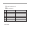
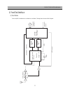
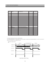
15 circuit operation manual memwait wait signal is produced in external device when accessing sram and peripheral devices. Wait signal is maintained as order status in the high status motivated by processor clock. Not_oe read strobe readnotwrite the ability to read or write of processing cycle. Acce...
Page 17
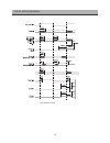
16 circuit operation manual emi interface timing.
Page 18
17 circuit operation manual 4. Front-end interface (1) tuner module tuner and qpsk demodulator are combined into one module. Following feature shows the block diagram. 2-wire bus control direct conversion zif t uner 4mhz 4mhz tda8260 inside lpf matched filter matched filter 2-wire bus control agc co...
Page 19
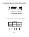
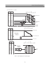
18 circuit operation manual data parity no error uncorrectible packet no error byte clk p a c k e t str out e r r o r by t e d a t a parallel data output timing ts output is made by the serial or parallel function. The relationship between ts output data and control signal is showing in the followin...
Page 20
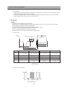
19 circuit operation manual sta r t bi t clk p a c k e t d7 e r r o r first bit of the packet data parity parity useful data 1 packet rs0 = 0 rs0 = 1 serial data output timing serial output timing (2) related with lnb. 1) lnb power and 22khz tone pulse the power supplied to lnb sends the 22khz tone ...
Page 21
20 circuit operation manual 2) loop through supports loop through for the interface function of other satellite devices. That means, in other satellite device, the control of lnb related voltage and tone are possible. If the signal of aux/ird control is in high status, the lnb voltage is provided fr...
Page 22
21 circuit operation manual 3) color bar cvbs, y, c, signals ma v 32.88 1.233 28.88 1.000 12.01 1.80 4.00 8.00 0.450 0.300 0.150 0.068 ma v 28.88 1.000 17.07 5.27 0.640 13.07 0.490 21.03 0.791 0.196 ma v 26.68 1.000 9.00 0.800 0.00 0.000 white yellow cyan green magenta red blue block 400 388 316 284...
Page 23
22 circuit operation manual 1-4) video output there are 2 video output port in the dsd-9251eav products. (tv scart, rca jack) the output of r,g and b signals are sent to tv scart through video buffer and lpf (low pass filter) originated from the sti5518 output. There are two control signals as of fa...
Page 24
23 circuit operation manual chart 81. Scart pinspec. 1) pcm audio audio related output of the sti5518 is made in the form of pcm format and ac3 interface format. Dsd-9251eav uses the serial data of pcm format. Pcm data output format is in standard format and i2s compatible pcm format. Followings are...
Page 25
24 circuit operation manual pcm timing analogue audio signals that are modified at audio dac are amplified by three times after going through low pass filter. The output is made after the amplification through av switch or buffer. 2) digital audio(spdif format) use pcm1754/texas instruments which ar...
Page 26
25 circuit operation manual a. Initialize multi-purpose pio port b. Sti5518 chip version detection c. Set dmt default multi-purpose pio port d. Initialize the os20 software scheduler e. Initialize the interrupt subsystem f. Flash vendor check g. Booting mode check(uart debugging mode / factory test ...
Page 27
26 circuit operation manual --- develop driver configuration --- [uartio fitted] [unhosted not fitted] [streport fitted] --- mpeg driver configuration --- [b_on_the_fly fitted] [enable_avsync fitted] [dont_blow_up_half_size_pictures not fitted] [built_for_16mbit fitted] [decode_elementary_stream not...
Page 28
27 circuit operation manual 7) teletext driver & process start teletext driver library v1.0 - version of apr 04 2000 at 01:34:03 creating teletext vbi task (priority=9) the teletext_data_transfer task is running creating teletext stb page filter task (priority=9) the ttx_stb_page_filter task is runn...
Page 29: Fixing Errors
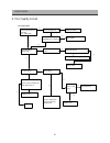
28 fixing errors (1) no response of display boot signal. 1. Booting led error start no display led signal. Yes yes no no no no no no no no yes yes yes yes yes yes yes a power on? Is reset ic working? Modify power status. Check reset circuit. Check 27mhz crystal and other peripheral circuit. Oscillat...
Page 30
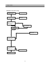
29 fixing errors (1) locking error 2. Poor quality screen check the power status of tuner(30v, vcc_tuner,3v3) 30v, 3v3 voltage ok? Tr(q808)ok?(vcc_tuner) replace the smps replace q808. Lnbp input control? Lnbp output ok?(ic27 pin3) eliminate problem causing factors. Replace lnbp check the power of l...
Page 31
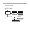
30 fixing errors (2)disabled screen after locking yes yes no no no no yes yes no yes yes yes no check the 3.3v power of tuner(ripple, voltage) fix the problem check error pin.(whether the output is in high status.) replace tuner tuner interface signal check? (ts_data, f_packet_clk, f_strt, f_b_clk) ...
Page 32
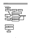
31 fixing errors (1) audio error 3. Errors in audio and video check the power status of audio dac eliminate problems check the input signal pcm data, sclk, lrclk, pcmclk) yes no yes no no check the sti 5518 check the interface of audio amp ic. Replace sti5518 replace audio dac eliminate problems rep...
Page 33
32 fixing errors (2) video error led booting ok sti5518 cvbs out check pin34 video buffer, low pass filter check confirm and execute the fixing process confirm the connection status of tracking port and execute the fixing process check the power status of sit5518 video (pin 23, pin30) check related ...
Page 34
33 bom list ✐ caution : in this service manual, some parts can be changed for improving their performance without notice in the parts list. So, if you need the latest parts information, please refer to ppl(parts price list)in service information center(http://svc.Dwe.Co.Kr) loc part code part name p...
Page 35
Bom list 34 loc part code part name part desc remark c415 hcqk391jba c chip cera 50v ch 390pf j 1608 c416 hcqk101jba c chip cera 50v ch 100pf j 1608 c418 hcbk392kba c chip cera 50v x7r 3900pf k 1608 c419 hcbk104kba c chip cera 50v x7r 0.1mf k 1608 c421 hcqk391jba c chip cera 50v ch 390pf j 1608 c422...
Page 36
35 bom list loc part code part name part desc remark q506 tktn2907 tr ktn2907 q507 t2sc5343sf tr chip 2sc5343sfg-dag q508 t2sc5343sf tr chip 2sc5343sfg-dag q509 tztc3875y- tr chip ktc3875y q510 t2sc5343sf tr chip 2sc5343sfg-dag q601 tktn2907 tr ktn2907 q602 t2sc5343sf tr chip 2sc5343sfg-dag q603 t2s...
Page 37
36 bom list loc part code part name part desc remark r334 hrfs103jba r chip 1/16 10k ohm j 1608 r335 hrfs103jba r chip 1/16 10k ohm j 1608 r336 hrfs103jba r chip 1/16 10k ohm j 1608 r339 hrfs103jba r chip 1/16 10k ohm j 1608 r340 hrfs102jba r chip 1/16 1k ohm j 1608 r341 hrfs103jba r chip 1/16 10k o...
Page 38
37 bom list loc part code part name part desc remark r625 hrfs121jba r chip 1/16 120 ohm j 1608 r626 hrfs221jba r chip 1/16 220 ohm j 1608 r627 hrfs221jba r chip 1/16 220 ohm j 1608 r702 hrfs330jba r chip 1/16 33 ohm j 1608 r707 hrfs330jba r chip 1/16 33 ohm j 1608 r708 hrfs330jba r chip 1/16 33 ohm...
Page 39
38 bom list loc part code part name part desc remark ap01 2193100801 solder wire sn:pb=63:37 3pi(no flux) ap02 2193011100 solder wire 60 sna 1.2d ap03 2291050305 flux liquid rf-800kn ap04 2291050306 flux thinner rf-800add ap05 2291140501 wax cover c801 cl2ee3104m c line across ac 275v 0.1mf m pcx2 3...
Page 40
39 bom list loc part code part name part desc remark aj02 2193011100 solder wire 60 sna 1.2d jk602 97p0s03000 jack sensor optic vst5b-12m p602 97p62k04e9 conn ffc scb-2109-m-2 09p st rf601 97p7214400 modulator rf ss m-gki1 u601 97p65442ja pcb jack 42x48.6(247x199/20) d1b loc part code part name part...
Page 41: Schematic Diagram
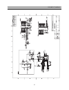
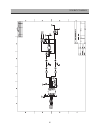
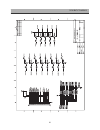
40 schematic diagram.
Page 42
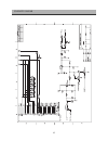
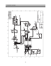
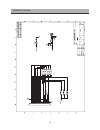
41 schematic diagram.
Page 43
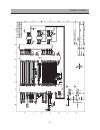
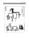
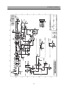
42 schematic diagram.
Page 44
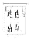
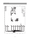
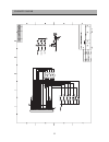
43 schematic diagram.
Page 45
44 schematic diagram.
Page 46
45 schematic diagram.
Page 47
46 schematic diagram.
Page 48
47 schematic diagram.
Page 49
48 schematic diagram.
Page 50
49 schematic diagram.
Page 51
50 schematic diagram.
Page 52
51 schematic diagram.
Page 53
52 schematic diagram.
Page 54: Parts Placement(Arrangement)
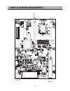
53 parts placement(arrangement).
Page 55
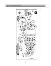
54 parts placement(arrangement).
Page 56
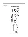
55 parts placement(arrangement) 9252 front pcb.
Page 57
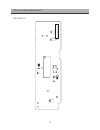
56 parts placement(arrangement) 9251 front pcb.
Page 58
57 parts placement(arrangement).
Page 59
686, ahyeon-dong mapo-gu seoul, korea c.P.O. Box 8003 seoul, korea daewoo electronics corp..


