- DL manuals
- Daewoo
- DVR
- DV-K82 series
- Service Manual
Daewoo DV-K82 series Service Manual - Section 2.
3
ADJUSTMENTS
SECTION 2.
ELECTRICAL ADJUSTMENTS
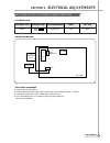
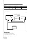
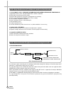
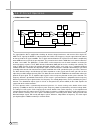
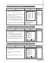
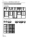
1. PLAYBACK PHASE
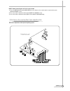
• CONNECTION METHOD
• ADJUSTMENT PROCEDURE
1) Play back the test tape. (DP-2)
2) Set the oscilloscope to the CHOP mode. Connect CH1 to the SW PULSE (PIN
3
of PT01).
3) Insert PATH JIG and Press “REC” button on the remote control.
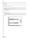
4) Check the position of the V-sync from the rising edge of the SW pulse.
(Standard : 6.5H
±
0.5H)
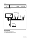
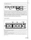
2-1. Servo Circuit Adjustment Method
ADJUSTMENT PARTS
Check
CHECKING POINT
JP037
PT01 PIN
4
Oscilloscope
MODE
Play
TEST TAPE
DP-2
V.OUT
TOP VIEW
PT01
PRE-AMP
CH-2
OSCILLOSCOPE
CH-1
PATH JIG
T
•
M
7
JP037
VIDEO OUT
MEASURING EQUIPMENT
Summary of DV-K82 series
Page 1
D a e w o o e l e c t r o n ic s c o l t d service manual video cassette recorder model : all k-mecha hi-fi pal models (dv-k88* series) (dv-k86* series) (dv-k82* series) (dv-k8k* series) daewoo electronics co., ltd. Overseas service dept..
Page 2
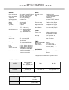
I n f o r m a t i o n s p e c i f i c at i o n general power requirement : ac 110-240v~, 50/60hz (for m.East) : ac 230v~, 50hz (for others) power consumption : max. 19w (in rec mode) temperature : 5˚c~35˚c (operating) -20˚c~60˚c operating position : horizontal only dimensions (wxhxd) : 360x90x288 (m...
Page 3: Video Cassette Recorder
Recorder video cassette recorder video cassette recorder video cassette recorder video cassette recorder vide cassette recorder video cassette recorder video cassette recorder video cassette recorder video casset recorder video cassette recorder video cassette recorder video cassette recorder video ...
Page 4: Section 1.
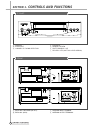
2 controls & functions section 1. Controls and functions front 1 stand by 2 stop/eject 3 channel up / down selection 4 play back 5 rewind / review 6 fast forward / cue 7 record / otr (one touch recording) rear 1 euro av2 / decoder (av out) 2 euro av1 (av in) 3 antenna input terminal 4 antenna output...
Page 5: Section 2.
3 adjustments section 2. Electrical adjustments 1. Playback phase • connection method • adjustment procedure 1) play back the test tape. (dp-2) 2) set the oscilloscope to the chop mode. Connect ch1 to the sw pulse (pin 3 of pt01). 3) insert path jig and press “rec” button on the remote control. 4) c...
Page 6
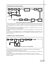
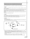
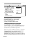
4 adjustments 1. Aft • aft connection method if module pcb (top view) 2-2. If module circuit adjustment methods adjustment parts l101 checking point p102 pin 7 test equipments signal gen. Oscilloscope power supply input signal refer to the following. P101 p102 gnd ch1 0.5ms/div 50mv/div(10:1) output...
Page 7
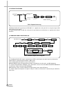
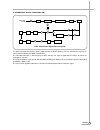
5 adjustments p101 p102 gnd ch1 0.5ms/div 0.1v/div(10:1) output signal modulation method : 30% am fm : 1khz fc : 38.9mhz signal level : 95db µ v gen. Gnd gnd power supply +9v +5v (component side) r191 l101 9 9 1 1 2.2 µ /50v 2. Rf agc • rf agc connection method if module pcb (top view) adjustment pa...
Page 8: Section 3.
6 1. Outline the part that supply dc voltage to each circuit change ac input voltage into dc voltage. It is based on smps(switching mode power supply)system which is located on main pcb. Smps module is composed of the switching circuit and the transformer of the primary part and the rectifier circui...
Page 9
7 3. General circuit operation the circuit shown is a highly accurate 38v, 12.5v, 6.0v, -24v, 4.5v, 20w secondary regulated flyback power supply that will operate from 85v to 265 vac input voltage. The input voltage is rectified and filtered by d801 and c1. L801, c801, c804 reduce conducted emissin ...
Page 10
8 circuit 1. La71511m(qop 80 pin) : luminance-chrominance and normal audio signal processing ic 1) applicable to multi system : pal-gbi, mesecam, 4.43ntsc, nap-gbi 2) built-in nap circuit to convert ntsc to pal 3) normal audio signal processing circuit (self-alignment for record bias) 4) built-in re...
Page 11
9 circuit 1) luminance signal processing (record) the input signal through fbc is reduced a half(-6db) of its level and then the pure luminance signal is obtained by lpf. In ynr(luminance noise reduction) circuit, noise is eliminated using the original signal and the 1h delayed signal. The detail en...
Page 12
10 circuit 2. Playback processing playback envelope signal from the pre-amp ic is supplied to the 15th pin of a/v ic for processing the pal color, luminance respectively. The output signal through y/c mix after each processing of chrominance and luminance is supplied to the 18th pin of osd ic. 1) lu...
Page 13
11 circuit 2) chrominance signal processing (pb) the down-converted chrominance signal is obtained from pb enve signal by lpf first. And then the signal is up- converted to 4.43mhz by the main converter. The redundant harmonics is filtered out by the bpf, and then the signal is applied to the ccd ic...
Page 14
12 1. Video signal flow the signal from the ant is amplified for selectivity, to decrease image interference, and increase s/n using the rf amp. The rf signal at the mixer is subtracted from the local osc frequency using the upperside band method, to change it into the if signal; 38.9mhz. The if sig...
Page 15
13 circuit 2. Pal audio flow (two carrier) the fm sound intercarrier signal passing through the 5.5mhz/5.74mhz (dk : 6.5mhz) sound bpf is fed to a limiter amplifier before it is demodulate. This gives high sensitivity and am suppression. The limiter amplifier consists of seven internal ac-coupled st...
Page 16
14 circuit 4. Tm block the tuner and modulator which is separated to each module conventionally, is presently united to one block (tm block) (a) pll method and i 2 c-bus control the rf output channel can be varied from 22ch to 69ch by remote control using pll method and i 2 c-bus control. Moreover, ...
Page 17
15 circuit the circuitry of normal audio part is similar to that of the conventional normal audio part in case of ee and pb mode, but in rec mode, due to the internal operation of self-alignment, it shows a lot of differences. 1. Ee mode la71511m has 3-input video/audio switching circuitry internall...
Page 18
16 circuit 3) the output audio signal at the 1st pin through rec amp is recorded on head after being mixed with the 70khz ac bias signal. At the same time, the output audio signal is supplied to the 3rd pin and then filtered by 60khz hpf, so only the 70khz ac bias signal is passed. The pure 70khz ac...
Page 19
2. Rec mode (1) signal flow in this system, the input signal sources are contained with if, av1, av2/c+ and f.Av. Each pin number’s decription is the same as the below. The input signals, selected by the input switcher, go through the lpf (at 20khz) and pnr processor. Additionally, the selected inpu...
Page 20
3. Pb mode (1) signal flow fm signal input to the pin 13rd is amplified, and ditributed to the two bpfs-1.4mhz and 1.8mhz. The band passed fm signals are supplied to the de-modulator unit. First, the fm lim confines the fm to the limitted level, and then the signals are demodulated. The converted au...
Page 21
19 circuit ant in 1 5 3 3 1 8 30 32 vcr tuner rf mod if block decoder in out tv ctl out in tv in out out in c+(l) 30 a b c d la7152 la71511m ka8119b 30 h h l l av3 ctl av4 ctl 5 38 29 5 4 f e f.Av in *ctl av1 av2 av3 av4 1. Ka8119b : special functions & features (1) internal audio/video switch for c...
Page 22
20 circuit 4. Switching operation in this switching system, video signals are selected by two a/v sw ics (ka8119b & la7152), audio signals are separately selectd by hi-fi ic itself which was controlled by the i 2 c bus. - w3d1, w3d2 mean the serial data bits for the selection. -refer below the table...
Page 23
21 circuit - case 1 tv set : watching & receiving the normal ch. Vcr set : power off, input source is turner. Tv set signal comes out to the decoder. - case 2 tv set : watching the c+ ch which is received by itself. Vcr set : power off, input source is tuner, discramble the c+ and supply it to the t...
Page 24
22 circuit - case 14 tv set : watching & receiving the normal ch. Vcr set : ee, tv mode. Input source is av. Tv set signal comes out to the decoder. - case 15 tv set : watching the c+ ch received on itself. Vcr set : tv mode. Input source is av. Discramble the c+ and supply it to the tv set. If a us...
Page 25
23 circuit (2) three input one output mode. (3) two input one output mode. Mode power off play ee/rec tv/vcr - - - tv vcr tv vcr tv vcr tv vcr tv vcr tuner /av1/av2 /f.Av tv av1 av2 - - tv av1 av2 f.Av c+ h l h l h l - - - - - - tv ctl l h l h l h l h l h l l l h l h av4 ctl l l l l l l h h h h h h ...
Page 26
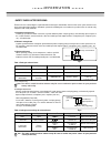
I n f o r m at i o n • safety check after servicing examine the area surrounding the repaired location for damage or deterioration. Observe that screws, parts and wires have been returned to original positions. Afterwards, perform the following tests and confirm the specified values in order to veri...
Page 27: Section 4.
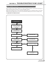
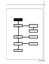
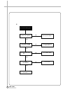
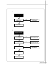
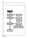
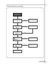
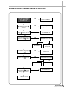
Flow chart section 4. Troubleshooting flow chart when changing the parts which are broken first, remove the power plug from the socket and then discharge the voltage across the terminals of c807 (use an external 1k Ω (2w) resistance). When check the primary circuit, use the oscilloscope isolated pro...
Page 28
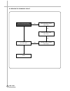
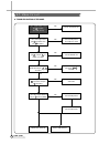
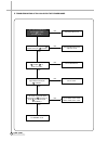
Flow chart check each output voltage end check the cn21 check the diode of no output stages check transformer of no output stages no check the coil, c of no output stages yes yes yes yes b. Checking the secondary circuit 25.
Page 29
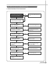
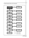
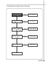
26 flow chart a. Troubleshooting of rf receiving circuit is video signal at video out point, p101 pin no. 4 of if module? Check the a/v switching and video circuit. Yes is audio signal at audio out point, p102 pin no.2/no.4 of if module? Yes no no yes yes yes yes is +5v supplied to bb point, pin no....
Page 30
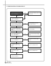
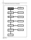
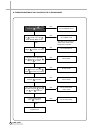
27 flow chart b. Troubleshooting of rf modulator out is video signal at video in point, pin no. 6 of tm block? Check the a/v switching, video and audio circuit. No is audio signal at audio in point, pin no. 2 of tm block? No yes yes yes yes yes yes are rf out system and rf out channel selected well ...
Page 31
28 flow chart 4-3. Logic circuit digitron is lit keys do not operate. Check key matrix circuit. Is each key pulse applied to pin 57 58 59 and 60 ic501? B. Check the pin serial of pin 49 , 50 of ic501 yes no digitron does not operate. Is +5.8v supplied from d509 cathod? Check power module check power...
Page 32
29 flow chart check and re-adjust the path of deck. Adjust the head height and remove dust. Check circuit adjacent to ic505 playback picture is not good adjust tracking. Noise appears although change cassette tape. Ctl head height is normal and there is not dust? Check r528, r527, r529, r523 check r...
Page 33
30 flow chart no no check flow a. Check d.Pg input and connector. Check pattern playback picture is not good. Noise appears on the screen at the bottom is sw pulse supplied from pin 18 of ic501? Noise appears on the screen on the whole. B. Are sw-pulse and ha-sw applied to preamp circuit? Yes check ...
Page 34
31 flow chart auto-stop during playback. Check reel sensor. Check connector and d. Fg circuits. Is reel pulse applied to pin 5 and 6 of ic501? C. Is d. Fg applied to pin 24 of ic501? Yes check ic501. Yes no no.
Page 35
32 flow chart drum m/t loading stops. Check q504 check power module. Is motor 12v supplied to ic502 7 8 pin 12v? D. Check connector and motor. Yes no no check d504. Is 6.2v supplied to pin 4 of ic502? Yes no check p503 and loading motor. Change ic502 yes no.
Page 36
33 flow chart capstan m/t loading stops. Check power module. Is motor 13v supplied? E. Check connector and motor. Yes no check circuit of r559, r558, r513. Is the input of pin 6 of p501 2.5v~3.5v? Yes no check ic501. Does pin 4 of ic501 supply c.Pwm? Yes check r555, r556. Is pin 4 of p501 2.5v? No y...
Page 37
34 flow chart drum m/t and capstan m/t rotate at regular speed. (in rec mode) check c.Sync of video ic and pattern. Is c. Sync applied to pin 93 of ic501? F. Check motor. No yes emergency mode when plugging (power cord) check power module. Is ever 5v applied? G. Check ic501. Yes no check ic501 and x...
Page 38
35 flow chart cassette is not inserted. Check power module. Is motor 13v supplied? (at pin 2 of cn21) h. Check ic502. No yes check connector. Check deck part. Cam data is changed when cst in? No no yes is 5v supplied at pin 31 of ic501? Check ic501. Check pattern and r549. Is 5v applied to pin 5 of ...
Page 39
36 flow chart power compensation does not operate. Check c501, c521. When mains is unplugged, is 3.6v at pin 26 76 and 81 of ic501? I. Check ic501. No yes check x502. Is (sine) signal applied to pin 42 and 43 of ic501? No yes check reset circuit of ic504. Is 5v at pin 37 of ic501? No yes.
Page 40
37 flow chart no sound in the playback mode is 5v applied to pin 76 of ic301 and is 5.8v applied to pin 2 of t201? Check power circuit is less then 0.2v at pin 80 of ic301? Is clock and data applied to pin 63, 64 of ic301? Is collector of q203 gnd? Check pattern and ac head check q203, q204, q202 ch...
Page 41
38 flow chart no check ic301 no check ic201 no no sound in the playback mode after recording check hi-fi, a/v select circuit check syscon is signal input into pin 73 of ic301? Yes is 5v applied to pin 76 of ic301 and is 5.8v applied to pin 2 of t201? Clean head yes yes yes yes yes yes yes no no no n...
Page 42
39 flow chart 4-6. Audio circuit (h i -f i ) no no sound in the ee mode check the power circuit. Is +5v supplied to the pin 18 36 of ic251? Is -5v supplied to the pin 39 of ic251? Yes yes no check the pif circuit. Is signal input into the pin 1 2 of ic251 in tv mode? Yes no is signal output at the p...
Page 43
40 flow chart no hi-fi sound in the playback mode is the fm enve supplied to the pin 13 of ic251? Is a. Sw pulse input to the pin 20 of ic251? Yes yes yes no check the power circuit. No change the ic251 no check the preamp module. No no check the syscon. Are the clock and data supplied to the pin 5 ...
Page 44
41 flow chart no is the signal obtained from pin 8 of ic602 (a/v sw. Circuit) check pcb pattern and adjacent circuit check on/off 5v is the video signal from pin 8 of ic602 fed to pin 30 of ic301? Yes is on/off 5v supplied to pin 36 and pin 47 of ic301 at 5 volts? To rf out circuit to a/v sw circuit...
Page 45
42 flow chart no is the signal from heads fed to pin 1 and pin 3 (lp mode) or pin 5 and pin 7 (sp mode) of p402? Check on/off 5v check rec(h) is on/off 5v from pin 76 of ic301 supplied to pin 13 of ic401 at 5 volts? Yes is rec(h) from pin 19 of ic301 supplied to pin 11 of ic401 at zero volt? Check v...
Page 46
43 flow chart no is the y-fm signal from pin 18 of ic301 fed to pin 9 of ic401? Check c315 and pattern check on/off 5v is the down converted colour signal from pin 14 of ic301 fed to pin 10 of ic401? Yes is on/off 5v supplied to pin 13 of ic401 at 5 volts? Change drum yes yes no check rec(h) is rec(...
Page 47
44 flow chart no is the video signal obtained from pin 8 of ic602 (av sw circuit)? Check on/off 5v yes is on/off 5v supplied to pin 36 and pin 47 of ic301 at 5 volts? To preamp circuit yes no is q302, q368, q369 and r308, r307, c312 correct? Change damaged components check ic301 check trick(h) check...
Page 48
45 flow chart is the video signal obtained from pin 8 of ic602 (a/v sw circuit)? Yes to preamp circuit check av sw circuit no no check on/off 5v is on/off 5v supplied to pin 36 and pin 47 of ic301 at 5 volts? Yes no check ic301 is the down-converted colour signal obtained from pin 14 of ic301? Yes n...
Page 49
46 flow chart is y-fm signal from pin 7 of ic401 fed to pin 15 of ic301? Yes to osd circuit check preamp circuit no no check q301, r301, r302 c306, c307, c308, l301 is the luminance signal from pin 15 of ic301 fed to pin 25 of ic301 through pin 17 and pin 20 ? Yes no check q302 and r309 is the lumin...
Page 50
47 flow chart no is the signal from pin 7 of ic401 fed to pin 15 of ic301? Check on/off 5v yes is on/off 5v supplied to pin 36 and pin 47 of ic301 at 5 volts? Yes no check ic301 is the pal colour signal from pin 15 of ic301 fed to pin 48 and pin 50 of ic301? Yes no change ic301 is the signal from pi...
Page 51: Section 5.
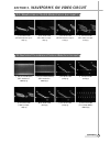
48 waveforms section 5. Waveforms on video circuit 5-1. Waveforms in the ee mode (color bar input) 1 pin 30 of ic301 (secam color bar input : 1.0vp-p) 2 pin 30 of ic301 (pal color bar input : 1.0vp-p) 3 pin 38 of ic301 (secam color bar output : 2.0vp-p) 4 pin 38 of ic301 (pal color bar output : 2.0v...
Page 52
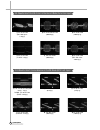
49 waveforms y pin 37 of ic301 (c.Sync : 2vp-p) u pin 14 of ic301 (300mvp-p) i pin 10 of ic401 (rec pal color : 300mvp-p) f up : pin 66 of ic301(color rotary : 1vp-p) down : pin 20 of ic301 (enve : 0.5vp-p) g pin 25 of ic301 (0.5vp-p) h pin 26 of ic301 (0.5vp-p) j pin 38 of ic301 (video out : 2.0vp-...
Page 53
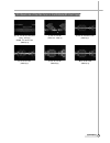
50 waveforms ; up : pin 66 of ic301(color rotary : 0.5vp-p) down : pin 20 of ic301 (500mvp-p) z pin 37 of ic301 (video out : 2.0vp-p) x pin 48 and 50 of ic301 (240mvp-p) c pin 52 of ic301 (300mvp-p) v pin 45 of ic301 (500mvp-p) b pin 46 of ic301 (500mvp-p) 5-5. Waveforms of the pal color in the pb m...
Page 54: Section 6.
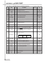
51 µ-com port section 6. µ-com port ic 501 (for u.K. & s/ireland:168kk8ykts, for others:168kk8x8ts) * p : pulse h : high l : low no. Name i/o assignment active cn 1 if on (h) o rf mode ‘h’ output otherwise ‘l’ output h pif 2 audio mute(h) o audio mute h output h video 3 d. Pwm o drum motor control p...
Page 55
52 µ-com port no. Name i/o assignment active cn tv/vcr mode switching on tv 27 tv control o tv mode : l, vcr mode : h l a/v sw active in digitron 28 canal + (l) i low input in canal broadcast l a/v sw 29 av2 o a/v input selector output h/l a/v sw 30 l/m r o l/h l/m ic 31 l/m f o cam data input * mod...
Page 56
53 µ-com port no. Name i/o assignment active cn 49 key in1 i key & option data input p 50 key in2 i key & option data input p 51 s0 o segment 0 52 s1 o segment 1 53 s2 o segment 2 54 s3 o segment 3 55 s4 o segment 4 56 s5 o segment 5 57 s6 o segment 6 58 s7 o segment 7 59 s8 o segment 8 60 s9 o segm...
Page 57
54 µ-com port no. Name i/o assignment active cn power when power is disconnected this port 85 fail (l) i detects power failure and then goes l into power compensation mode 86 start sensor i tape start sensor data input a/d start sensor 87 drum sel i a/d 88 aft i aft analog data input for auto fine t...
Page 58: Section 7.
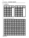
55 voltage charts section 7. Voltage charts voltage charts tda9814t for if ic (ic101) mode pin no. 1 2 3 4 5 6 7 8 9 10 11 12 13 14 two carrier 3.3 3.3 0.8 1.1 2.5 2.7 3.0 2.2 3.5 2.3 2.3 2.2 2.0 1.9 nicam 3.3 3.3 0.8 0.7 2.5 2.9 3.0 2.0 3.5 2.5 2.4 1.7 2.1 2.1 remarks conditions : ee mode mode pin ...
Page 59
56 voltage charts pin no. 1 2 3 4 5 6 7 8 9 10 11 12 13 14 15 rec 0.00 2.62 2.63 0.00 0.00 0.00 0.00 (2.2) (2.0) (2.2) 5.00 5.00 5.00 5.00 4.50 pb 0.00 2.62 2.64 0.00 0.00 0.00 0.00 (2.2) (2.0) (2.2) 5.01 5.01 5.01 5.01 4.50 pin no. 16 17 18 19 20 21 22 23 24 25 26 27 28 29 30 rec 1.99 5.00 2.00 2.0...
Page 60
57 voltage charts av sw ic (ic602) pin no 1 2 3 4 5 6 7 8 9 play 2.54 5.12 2.55 0.82 0.00 2.59 0.00 1.10 5.12 ee 3.12 5.05 3.12 0.82 0.00 2.59 0.00 1.69 5.05 pin no. 1 2 3 4 5 6 7 8 9 10 11 12 13 14 15 16 17 18 19 20 21 22 rec 0.00 0.00 0.00 0.00 4.63 4.50 0.00 2.45 -4.85 0.00 0.00 0.00 0.00 0.73 0....
Page 61
58 voltage charts ba6209 for m/t drive ic (ic502) 24lc08b for eeprom ic (ic503) pin no 1 2 3 4 5 6 7 8 9 10 rec 0 0.5 0.84 6.1 0 0 12.3 12.3 0.86 0.5 pb 0 0.5 0.84 6.1 0 0 12.5 12.5 0.86 0.5 pin no 1 2 3 4 5 6 7 8 rec 0 0 0 0 5.26 0 4.71 4.71 pb 0 0 0 0 5.26 0 4.71 4.71 k1a7033p for reset ic (ic504)...
Page 62
59 voltage charts if module part tr ports loc. Q101 q102 two carrier - 1.5 nicam 0.3 1.4 two carrier - 5.0 nicam 7.0 5.0 two carrier - 2.1 nicam 1.0 2.1 emitter collector base audio part tr ports loc. Q201 q202 q203 q204 q205 pb 5.4 5.19 0 0 0 rec 1.82 5.2 -23.44 -23.44 0.02 pb 5.9 5.16 0.01 0 5.43 ...
Page 63
60 voltage charts power part tr ports loc. Q811 q816 q812 q815 q813 q814 power on 10.43 10.43 5.18 5.18 0.0 -9.6 power off 10.4 10.4 0.25 0.25 0.0 -9.7 power on 12.6 12.6 5.94 5.94 5.8 -17.2 power off 12.2 12.2 6.4 6.4 0.06 -22.3 power on 11.0 11.0 5.88 5.88 0.0 -10.25 power off 11.0 11.0 0.06 0.06 ...
Page 64: Section 8.
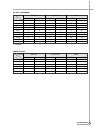
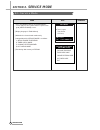
Item 1 press the [menu] button to go to [main menu] screen and press the number 484 in sequence then go to [service mode] screen. 2 display language is english only. 3 maintain the selected mode continuously. 4 composition of the service mode is as follows. 1) service mode for repair 2) timer check ...
Page 65
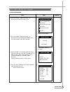
62 service mode item 1 press the number 1 button, then osd 1 is displayed in the initial svc mode screen. 2 press the number 3 button, then osd 2 is displayed in the svc mode for repair screen. It can be selected in tape out state only. 3 pal test tape is inserted after guide message is appeared, pl...
Page 66
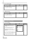
63 service mode item * timer check mode is used to check the timer record/showview record and vfd segment. 1 press the number 2 button, then osd 1 will be displayed in the initial svc mode screen. 2 press the number 1 button, fast clock operation will be selected in the timer check mode screen. * th...
Page 67
64 service mode item * change of eeprom data mode is used for change the video/audio characteristic data. 1 press the number 3 button, osd 1 will be displayed in the initial svc mode screen. 2 press the [ ] button to move from right to left. 3 press the [ ➔ ] button to move from upper to lower. 4 pr...
Page 68
65 service mode 8-8. The method to initialize the eeprom 8-7. H i- f i check mode 1. When [484] is sequentially pressed in menu mode, the service mode is activated. 2. Choose “change of eeprom data” by pressing [3]. 3. The input video signal should be pal or null signal, and the speed should be sp. ...
Page 69
66 ser vice mode 8-10. Sanyo a/v 1 chip serial control table address bit 0000 0001 group 1 common 0000 0010 group 2 commom 0000 0011 group 3 common 0000 0100 group 4 rec 0000 0101 group 5 common 0000 0110 group 6 pb 0000 0111 group 7 pb 0000 1000 group 8 pb 0000 1001 group 9 audio 8 7 00 auto color ...
Page 70
67 service mode 8-11. Sanyo a/v 1chip serial data (pal 4h’d) pal sp ee/rec/pb group 1 0 0 0 1 1 1 group 2 1 1 1 1 1 1 1 0 group 3 1 0 0 0 0 0 1 0 group 4 1 0 1 0 0 1 1 1 group 5 0 1 0 1 1 0 1 1 group 6 1 0 0 0 1 0 1 0 group 7 0 0 0 0 1 0 0 0 group 8 1 0 0 1 1 0 0 0 group 9 1 0 0 0 1 0 ➜ 8 7 6 5 4 3 ...
Page 71
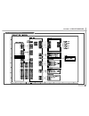
68 circuit diagrams 9-1. Connection diagram section 9. Circuit diagram 68.
Page 72
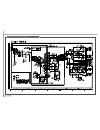
69 circuit diagrams r819 5.1 9-2. Power circuit diagram.
Page 73
70 circuit diagrams 9-3. Syscon and logic circuit diagram.
Page 74
71 circuit diagrams 9-4. Av sw circuit diagram.
Page 75
72 circuit diagrams 9-5. If/pdc circuit diagram (tm).
Page 76
73 circuit diagrams 9-6. If module circuit diagram (a2).
Page 77
74 circuit diagrams 9-7. If module circuit diagram (nicam).
Page 78
75 circuit diagrams 9-8. H i -f i /pre-amp circuit diagram.
Page 79
76 circuit diagrams 9-9. Video/audio circuit diagram.
Page 80
77 circuit diagrams 9-10. Remocon circuit diagram.
Page 81
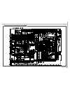
Section 10. Components location guide on pcb bottom view 78 p.C.B. Location 10-1. Pcb main.
Page 82
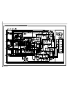
80 p.C.B. Location 10-3. Pcb logic dv-k8k ƒ ƒs s series dv-k86 ƒ ƒs s series (dv-k82 ƒ ƒs s series).
Page 83
81 p.C.B. Location dv-k88 ƒƒ ss series.
Page 84
Section 11. Disassembly 83 disassembly 11-1. Packing ass’y.
Page 85
84 diagrams dv-k88 series * dv-k82 series * dv-k8k series * dv-k86 series * 11-2. Front panel assembly.
Page 86
68 circuit diagrams 9-1. Connection diagram section 9. Circuit diagram 68.
Page 87
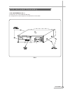
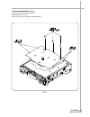
85 disassembly 1. Top cover removal (fig. 1) 1) remove five (5) screws holding the top cover. 2) carefully lift the back of the top cover and slide to the rear to remove. 11-3. Instrument disassembly fig. 1.
Page 88
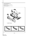
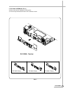
86 disassembly 2. Front panel removal (fig. 2) 1) remove the top cover. 2) remove two (2) screws securing front panel. 3) remove the f/l bracket. 4) release seven (7) tabs holding the front panel. 5) remove the front panel. Dv-k88 series dv-k82 series dv-k86 series dv-k8k series * * * * fig. 2.
Page 89
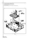
87 disassembly 3. Bottom cover removal (fig. 3) 1) remove the top cover and front panel. 2) remove three (3) screws. 3) release four (4) tabs and lift out the bottom cover. Fig. 3.
Page 90
88 disassembly 4. F/l door removal (fig. 4) 1) open the f/l door 90˚. 2) remove the f/l door in the direction of arrow. Fig. 4.
Page 91
89 disassembly 5. Pcb logic as removal (fig. 5) 2) release two (2) tabs holding the pcb logic as. 3) tilt pcb logic as forward to remove in the direction of arrow. Dv-k82 series dv-k86 series dv-k8k series * * * dv-k88 series * fig. 5.
Page 92
90 disassembly 6. Cover pre-amp/deck as removal (fig. 6) 1) remove the top cover, bottom cover and front panel. 2) remove five (5) screws. 3) pull out the deck as and cover pre-amp in the direction of arrow. Fig. 6.
Page 93
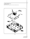
91 disassembly 7. Pcb main as removal (fig. 7) 1) remove two (2) screws. 2) release three (3) tabs and lift out the main pcb in the direction of the arrow. Fig. 7.
Page 94: Section 12.
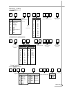
92 parts list section 12. Electrical parts list 12-1. Standard parts number coding resistor coding 1. Fixed resistor coding 2. Semi-fixed resistor conding r type of resistor c composition resistor d carbon resistor f fusible resistor k ceramic resistor n metal film resistor s metal-oxide film resist...
Page 95
93 parts list capacitor coding fuse coding 1. Normal 2. Temperature compensation c type code tpye a aluminum b barrier layer c ceramic e electrolytic l line across m mylar s styrol n metalized polyester q mica oil t tantal distance code voltage 0j 6.3v 1a 10v 1c 16v 1d 20v 1e 25v 1v 35v 1g 40v 1h 50...
Page 96
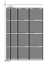
94 parts list pcb main as loc part code part name part description 23 97pd183900 pcb main as dv-k884dy-aq *b001b 97p0974800 plate earth tmi sus304 csp t0.2 c801 cl1ue3104m c line across ac275v 0.1mf m 1.40 world c804 ch1cee472m c cera ac 2.5kv 4700pf m de ac250v c805 ch1cfb101k c cera ac 4.0kv 100pf...
Page 97
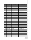
95 parts list loc part code part name part description t201 560202l692 coil osc deo-006 x301 5xe4r4336b crystal quartz hc-49/u 4.433619mhz 15ppm x502 5xzr03276g crystal quartz so-26 32.768000khz 10ppm 31 97pb227600 pcb main chip as dv-k884dy-aq c001 hcbk103kca c chip cera 50v x7r 0.01mf k 2012 c003 ...
Page 98
96 parts list loc part code part name part description c314 hcbk103kca c chip cera 50v x7r 0.01mf k 2012 c319 hcbk103kca c chip cera 50v x7r 0.01mf k 2012 c323 hcfk104zca c chip cera 50v y5v 0.1mf z 2012 c328 hcbk103kca c chip cera 50v x7r 0.01mf k 2012 c329 hcfk104zca c chip cera 50v y5v 0.1mf z 20...
Page 99
97 parts list loc part code part name part description c820 hcbk103kca c chip cera 50v x7r 0.01mf k 2012 c821 hcbk103kca c chip cera 50v x7r 0.01mf k 2012 c824 hcbk103kca c chip cera 50v x7r 0.01mf k 2012 ic251 1bh7804k-- ic hifi bh7804k ic301 1la71511m- ic a/v la71511m ic302 1lc89977m- ic ccd lc899...
Page 100
98 parts list loc part code part name part description r182 hrft103jca r chip 1/10 10k ohm j 2012 r184 hrft303jca r chip 1/10 30k ohm j 2012 r185 hrft103jca r chip 1/10 10k ohm j 2012 r186 hrft183jca r chip 1/10 18k ohm j 2012 r190 hrft563jca r chip 1/10 56k ohm j 2012 r201 hrft334jca r chip 1/10 33...
Page 101
99 parts list loc part code part name part description r504 hrt511jca r chip 1/10 510 ohm j 2012 r505 hrft511jca r chip 1/10 510 ohm j 2012 r506 hrt304jca r chip 1/10 300k ohm j 2012 r510 hrft331jca r chip 1/10 330 ohm j 2012 r511 hrft331jca r chip 1/10 330 ohm j 2012 r512 hrft331jca r chip 1/10 330...
Page 102
100 parts list loc part code part name part description r631 hrft561jca r chip 1/10 560 ohm j 2012 r632 hrft561jca r chip 1/10 560 ohm j 2012 r633 hrft561jca r chip 1/10 560 ohm j 2012 r634 hrft561jca r chip 1/10 560 ohm j 2012 r635 hrft561jca r chip 1/10 560 ohm j 2012 r636 hrft561jca r chip 1/10 5...
Page 103
101 parts list loc part code part name part description c255 cmxm2a472j c mylar 100v 4700pf j (tp) c256 cexf1a101a c electro 10v rsm 100mf 6.3x7 c257 cexf1a101a c electro 10v rsm 100mf 6.3x7 c258 cmxm2a472j c mylar 100v 4700pf j (tp) c260 cmxm2a223j c mylar 100v 0.022mf j tp c261 cexf1h100a c electr...
Page 104
102 parts list loc part code part name part description c620 cexf1a471v c electro 10v rss 470mf 8x11.5 c625 cexf1e220a c electro 25v rsm 22mf 6.3x7 c626 cexf1e220a c electro 25v rsm 22mf 6.3x7 c627 cexf1e220a c electro 25v rsm 22mf 6.3x7 c628 cexf1e220a c electro 25v rsm 22mf 6.3x7 c629 cexf1c470a c...
Page 105
103 parts list loc part code part name part description q178 tzsr1001-- tr ksr1001 (auto) q179 tzta1273y- tr kta1273y(966y) q180 tzsr1001-- tr ksr1001 (auto) q181 tztc3198y- tr ktc3198y-(1815y) (auto) q201 tztc3202y- tr ktc3202y (auto)(1959y) q202 tzta1266y- tr kta1266y- (auto)(1015y) q203 tztc3198y...
Page 106
104 parts list loc part code part name part description c321 cczf1h104z c cera hikf 50v 0.1mf z axial c334 cbzp1c103m c cera semi 16v y5s 0.01mf m (axial) c340 cczf1h104z c cera hikf 50v 0.1mf z axial c341 cbzp1c103m c cera semi 16v y5s 0.01mf m (axial) c342 cbzp1c103m c cera semi 16v y5s 0.01mf m (...
Page 107
105 parts list loc part code part name part description d618 dzz5r6bm-- diode zener dz 5.6bm (auto) d619 dzz5r6bm-- diode zener dz 5.6bm (auto) d620 dzz5r6bm-- diode zener dz 5.6bm (auto) d621 dzz5r6bm-- diode zener dz 5.6bm (auto) d622 dzz5r6bm-- diode zener dz 5.6bm (auto) d623 dzz5r6bm-- diode ze...
Page 108
106 parts list loc part code part name part description jp023 85801065gy wire copper awg22 1/0.65 tin coating jp024 85801065gy wire copper awg22 1/0.65 tin coating jp025 85801065gy wire copper awg22 1/0.65 tin coating jp026 85801065gy wire copper awg22 1/0.65 tin coating jp027 85801065gy wire copper...
Page 109
107 parts list loc part code part name part description jp074 85801065gy wire copper awg22 1/0.65 tin coating jp075 85801065gy wire copper awg22 1/0.65 tin coating jp076 85801065gy wire copper awg22 1/0.65 tin coating jp077 85801065gy wire copper awg22 1/0.65 tin coating jp078 85801065gy wire copper...
Page 110
108 parts list loc part code part name part description jp124 85801065gy wire copper awg22 1/0.65 tin coating jp125 85801065gy wire copper awg22 1/0.65 tin coating jp126 85801065gy wire copper awg22 1/0.65 tin coating jp127 85801065gy wire copper awg22 1/0.65 tin coating jp128 85801065gy wire copper...
Page 111
109 parts list loc part code part name part description jp173 85801065gy wire copper awg22 1/0.65 tin coating jp174 85801065gy wire copper awg22 1/0.65 tin coating jp175 85801065gy wire copper awg22 1/0.65 tin coating jp176 85801065gy wire copper awg22 1/0.65 tin coating jp177 85801065gy wire copper...
Page 112
110 parts list loc part code part name part description jp222 85801065gy wire copper awg22 1/0.65 tin coating jp223 85801065gy wire copper awg22 1/0.65 tin coating jp224 85801065gy wire copper awg22 1/0.65 tin coating jp225 85801065gy wire copper awg22 1/0.65 tin coating jp226 85801065gy wire copper...
Page 113
111 parts list loc part code part name part description jp274 85801065gy wire copper awg22 1/0.65 tin coating jp275 85801065gy wire copper awg22 1/0.65 tin coating jp276 85801065gy wire copper awg22 1/0.65 tin coating jp277 85801065gy wire copper awg22 1/0.65 tin coating jp278 85801065gy wire copper...
Page 114
112 parts list loc part code part name part description r267 rd-az561j- r carbon film 1/6 560 ohm j r268 rd-az101j- r carbon film 1/6 100 ohm j r269 rd-az101j- r carbon film 1/6 100 ohm j r272 rd-az101j- r carbon film 1/6 100 ohm j r273 rd-az101j- r carbon film 1/6 100 ohm j r276 rd-az513j- r carbon...
Page 115
113 parts list loc part code part name part description r558 rd-az103j- r carbon film 1/6 10k ohm j r559 rd-az362j- r carbon film 1/6 3.6k ohm j r560 rd-az473j- r carbon film 1/6 47k ohm j r561 rd-az331j- r carbon film 1/6 330 ohm j r562 rd-az331j- r carbon film 1/6 330 ohm j r571 rd-az331j- r carbo...
Page 116
114 parts list table of difference part list main as 1. For emc & micom 4. Power cord as loc part-code for others for u.K. & s/ireland b001b 97p7608300 delete add ic501 --- s/n : 168kk8x8ts s/n : 168kk8ykts 2. For a/v jack & c807 loc part-code for others for australia & m.East jk601 97p6313300 add d...
Page 117
115 parts list pcb logic as loc part code part name part description 24 97pd184200 pcb logic sw as dv-k884dy-aq g701 dsvv6ss25- digitron (v.F.D) svv-6ss25 h701 1gp3u771r- ic unit r/receiver gp3u771r jk701 97p6311300 jack pin dsp-9407a jk71a 97p0973700 plate earth av sus304 csp t0.15 m701 97p2340500 ...
Page 118
116 parts list loc part code part name part description jp717 85801065gy wire copper awg22 1/0.65 tin coating jp718 85801065gy wire copper awg22 1/0.65 tin coating jp720 85801065gy wire copper awg22 1/0.65 tin coating jp721 85801065gy wire copper awg22 1/0.65 tin coating jp722 85801065gy wire copper...
Page 119
117 parts list loc part code part name part description 25 97pd184200 pcb if module as(a2) dv-k884dy-aq ic121 1tda9845-- ic rf tda9845 l101 56b215k694 coil pif ktrf-7780b p101 97p62m05a9 conn b/b 35238 recep 2.5mm 9p p102 97p62m05a9 conn b/b 35238 recep 2.5mm 9p x121 5xe10r000c crystal quartz hc-49/...
Page 120
118 parts list loc part code part name part description c116 cexf1e470v c electro 25v rss 47mf (5x11) tp c121 cexf1e470v c electro 25v rss 47mf (5x11) tp c123 cmxm2a104j c mylar 100v 0.1mf j (tp) c124 cmxm2a182j c mylar 100v 1800pf j (tp) c126 cexf1h229v c electro 50v rss 2.2mf (5x11) tp c127 cexf1h...
Page 121
119 parts list loc part code part name part description 22 97pd186100 pcb if as (nicam) dv-k884dy-aq/i ic102 1saa7283zp ic rf saa7283zp (nicam) l101 56b215k694 coil pif ktrf-7780b p101 97p62m05a9 conn b/b 35238 recep 2.5mm 9p p102 97p62m05a9 conn b/b 35238 recep 2.5mm 9p x102 5xe08r192c crystal quar...
Page 122
120 parts list loc part code part name part description c148 hcbk223kca c chip cera 50v x7r 0.022mf k 2012 c149 hclk100dca c chip cera 50v sl 10pf d 2012 c150 hcqk101jca c chip cera 50v ch 100pf j 2012 c151 hcqk101jca c chip cera 50v ch 100pf j 2012 c152 hcfk104zca c chip cera 50v y5v 0.1mf z 2012 c...
Page 123
121 parts list loc part code part name part description q102 tztc3198y- tr ktc3198y-(1815y) (auto) r191 rv5426203m r semi fixed h20k-5x3-6y-pc-ms 01a 97pa491500 pcb if a-auto(nicam) dv-k884dy-aq/i d101 dzn4148--- diode 1n4148 auto 52mm d102 dzbb405--- diode varactor bb405 jp001 85801065gy wire coppe...
Page 124
122 parts list loc part code part name part description 26 97pd184300 pcb pre amp as dv-k884dy-aq ic401 1la70011-- ic preamp la70011 (4hd) m401 97pb227500 case pre amp as dv-k884dy-aq m401a 97p0470300 cover shi preamp et t0.3 m401b 97p0470200 case shi preamp et t0.4 p401 97p62g01bf conn b/b gb200 re...
Page 125
123 parts list loc part code part name part description jp401 85801065gy wire copper awg22 1/0.65 tin coating jp402 85801065gy wire copper awg22 1/0.65 tin coating jp403 85801065gy wire copper awg22 1/0.65 tin coating jp410 85801065gy wire copper awg22 1/0.65 tin coating jp411 85801065gy wire copper...
Page 126
124 parts list pcb power smps as loc part code part name part description 27 97pd184000 pcb power smps as dv-k884dy-aq a01 2193102005 solder bar sn:pb=63:47 s63s-1320 a02 2193011100 solder wire 60 sna 1.2d a03 2291050615 flux solder ks-892m-1 a04 2291050312 flux solvent s-3000d b01 97p0465700 cover ...
Page 127
125 parts list loc part code part name part description c25 cexf1j220d c electro 63v rz 22mf 6.3x11.5 tp c26 cexf1h220v c electro 50v rss 22mf (5x11) tp ic21 1ka431az-- ic regulator ka431az 54 97pa490600 pcb power a-auto as dv-k884dy-aq dz12 dzz6r8bm-- diode zener uz-6.8bm auto d12 dzeu01z--- diode ...
Page 128: Section 13.
126 service jig fixture item description p/n extension cable 1 use for k mecha drum motor connection cable 97pb400100 extension cable 2 use for k mecha capstan motor connection cable 97pb400200 extension cable 3 use for k mecha a/c head and l/c motor connecting cable 97pb400300 path adj fixture use ...
Page 129
127 service jig path fixture connection/test point identification connect to pt01 1 pin ~ 7 pin of the main circuit board refer to the adjustment of the tape transporting system note : how to executing the unit in the service mode 1) press the [menu] button to go to [main menu] screen and press the ...


