Summary of EV10AS150A
Page 1
Adc ev10as150a evaluation board user guide.
Page 2
2 adc ev10as150a user guide 0977b–bdc–09/09.
Page 3
Ev10as150a-eb user guide 1 0977b–bdc–10/09 table of contents section 1 introduction ........................................................................................... 1-1 1.1 scope1-1 1.2 description ..............................................................................................
Page 4
2 ev10as150a-eb user guide 0977b–bdc–10/09 section 7 ordering information............................................................................. 7-1 section 8 appendix............................................................................................... 8-1 8.1 ev10as150a-eb electrica...
Page 5: Section 1
Ev10as150a-eb user guide 1-1 0977b–bdc–10/09 e2v semiconductors sas 2009 section 1 introduction 1.1 scope the adc ev10as150a-eb evaluation kit is designed to facilitate the evaluation and characterization of the different versions of ev10as150a adc with 1:2/4 dmux up to its 5 ghz full power input ba...
Page 6
Introduction 1-2 ev10as150a-eb user guide 0977b–bdc–10/09 e2v semiconductors sas 2009 the board is composed of eight metal layers for signal traces, ground and power supply layers, and seven dielectric layers featuring low insertion loss and enhanced thermal characteristics for operation in the high...
Page 7: Section 2
Ev10as150a-eb user guide 2-1 0977b–bdc–10/09 e2v semiconductors sas 2009 section 2 hardware description 2.1 board structure in order to achieve optimum full speed operation of the adc ev10as150a with 1:2/4 dmux, a multilayer board structure was retained for the evaluation board. Eight copper layers ...
Page 8
Hardware description 2-2 ev10as150a-eb user guide 0977b–bdc–10/09 e2v semiconductors sas 2009 the board is 1.6 mm thick. The clock, analog input, reset and digital data output signals occupy the top metal layer while the adc and dmux functions are located both on the top. The ground planes occupy la...
Page 9
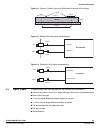
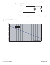
Hardware description ev10as150a-eb user guide 2-3 0977b–bdc–10/09 e2v semiconductors sas 2009 figure 2-1. Figure 2-1.Board layout for the differential analog and clock inputs figure 2-2. Differential analog inputs implementation figure 2-3. Differential clock inputs implementation 2.3 digital output...
Page 10
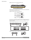
Hardware description 2-4 ev10as150a-eb user guide 0977b–bdc–10/09 e2v semiconductors sas 2009 figure 2-4. Board layout for the differential digital outputs the digital outputs are compatible with lvds standard. They are on-board 100 Ω differ- entially terminated as described in figure 2-5. Figure 2-...
Page 11
Hardware description ev10as150a-eb user guide 2-5 0977b–bdc–10/09 e2v semiconductors sas 2009 2.4 reset lines the reset line (drr and asyncrst) were designed with the following recommendations: 50 Ω lines 80 mm max line length 430 µm line width 40 µm thickness figure 2-8. Board layout for th...
Page 12
Hardware description 2-6 ev10as150a-eb user guide 0977b–bdc–10/09 e2v semiconductors sas 2009.
Page 13: Section 3
Ev10as150a-eb user guide 3-1 0977b–bdc–10/09 e2v semiconductors sas 2009 section 3 operating characteristics 3.1 introduction this section describes a typical configuration for operating the evaluation board of the adc ev10as150a with 1:2/4 dmux. The analog input signal can be entered either in diff...
Page 14
Operating characteristics 3-2 ev10as150a-eb user guide 0977b–bdc–10/09 e2v semiconductors sas 2009 9. Perform an asynchronous reset (drr active) on the device and maintain this reset active. 10. Perform an asynchronous reset ((push button) asyncrst active) on the board. 11. Then, asyncrst inactive o...
Page 15
Operating characteristics ev10as150a-eb user guide 3-3 0977b–bdc–10/09 e2v semiconductors sas 2009 note: absolute maximum ratings are limiting values (referenced to gnd = 0v), to be applied individually, while other parameters are within specified operating conditions. Long exposure to maximum ratin...
Page 16
Operating characteristics 3-4 ev10as150a-eb user guide 0977b–bdc–10/09 e2v semiconductors sas 2009 3.4 digital output coding msb bit 9 and lsb bit 0. Note: 1. Refer to chap. 4.4.4 and 4.4.5 for selection between natural binary, binary 2's complement or gray coding. Table 3-3. Digital output coding d...
Page 17: Section 4
Ev10as150a-eb user guide 4-1 0977b–bdc–10/09 e2v semiconductors sas 2009 section 4 software tools 4.1 overview the adc ev10as150a evaluation user interface software is a c++ compiled graphical interface. No license is required to run on a w98, nt, w2000 and xp pc. The software uses intuitive push bu...
Page 18
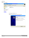
Software tools 4-2 ev10as150a-eb user guide 0977b–bdc–10/09 e2v semiconductors sas 2009 figure 4-1. Install window start the setup_ev10as15x (v1.1.2) figure 4-2. Ev10as150a application set up wizard window.
Page 19
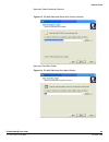
Software tools ev10as150a-eb user guide 4-3 0977b–bdc–10/09 e2v semiconductors sas 2009 next step: select destination directory. Figure 4-3. Ev10as150a select destination directory window next step: start menu folder. Figure 4-4. Ev10as150a select start menu window.
Page 20
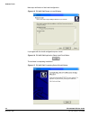
Software tools 4-4 ev10as150a-eb user guide 0977b–bdc–10/09 e2v semiconductors sas 2009 next step: verification of the install configuration. Figure 4-5. Ev10as150a ready to install window if you agree with the install configuration press install. Figure 4-6. Ev10as150a application setup install pus...
Page 21
Software tools ev10as150a-eb user guide 4-5 0977b–bdc–10/09 e2v semiconductors sas 2009 now you can launch the adc10bit series software from its icon; the following screen will be displayed: figure 4-8. Adc ev10as150a user interface window figure 4-9. Adc10-bit user interface hardware implementation...
Page 22
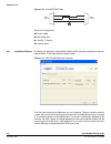
Software tools 4-6 ev10as150a-eb user guide 0977b–bdc–10/09 e2v semiconductors sas 2009 figure 4-10. Crossed rs232 cable serial port configuration: bit rate: 19200 data coding: 8 bit 1 start bit, 1 stop bit no parity check 4.3.1 installation software at startup, the application automatically...
Page 23
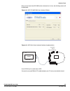
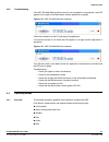
Software tools ev10as150a-eb user guide 4-7 0977b–bdc–10/09 e2v semiconductors sas 2009 4.3.2 troubleshooting if the adc ev10as150a evaluation board is not connected or not powered, a red led appears on the right of the reset button and the application is grayed figure 4-12. Adc ev10as150a user inte...
Page 24
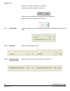
Software tools 4-8 ev10as150a-eb user guide 0977b–bdc–10/09 e2v semiconductors sas 2009 always click on apply to validate any command each setting must be validated in its own tab. Clicking on cancel will restore last settings sent with apply button. Reset button allows to configure adc (mode 0) 4.4...
Page 25
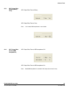
Software tools ev10as150a-eb user guide 4-9 0977b–bdc–10/09 e2v semiconductors sas 2009 4.4.3 adc output data format (binary- gray) adc output data format: binary adc output data format: gray note: in this mode, msb complement is not available. 4.4.4 adc output data format (msb complement) adc outpu...
Page 26
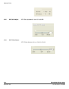
Software tools 4-10 ev10as150a-eb user guide 0977b–bdc–10/09 e2v semiconductors sas 2009 4.4.5 adc gain adjust adc gain adjustment is from –0.5 to 0.5 db. 4.4.6 adc offset adjust adc offset adjustment is from –20 mv to 20 mv..
Page 27
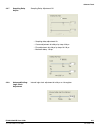
Software tools ev10as150a-eb user guide 4-11 0977b–bdc–10/09 e2v semiconductors sas 2009 4.4.7 sampling delay adjust sampling delay adjustment off – sampling delay adjustment on – coarse adjustment: 0 to 90 ps by step of 30 ps – fine adjustment: 0 to 30 ps by step of 0.118 ps – maximum delay: 120 ps...
Page 28
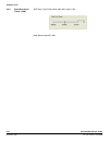
Software tools 4-12 ev10as150a-eb user guide 0977b–bdc–10/09 e2v semiconductors sas 2009 4.4.9 clock duty cycle (track - hold) adc duty cycle (track-hold): 40%-60% to 30%-70% note: reset value 35%-65%.
Page 29: Section 5
Ev10as150a-eb user guide 5-1 0977b–image–10/09 e2v semiconductors sas 2009 section 5 application information 5.1 introduction for this section, refer also to the product chapter 4 of the datasheet. 5.2 analog inputs the analog input can be entered either single ended or differentially. Refer to the ...
Page 30
Application information 5-2 ev10as150a-eb user guide 0977b–image–10/09 e2v semiconductors sas 2009 5.5 adc functions 5.5.1 drr (data ready reset) the data ready reset signal is accessed via an sma connector. Drr is cmos/lvcmos compatible: v il = 0 (typical) v ih = v cca3 (typical) the active lev...
Page 31
Application information ev10as150a-eb user guide 5-3 0977b–image–10/09 e2v semiconductors sas 2009 5.6.2 clkdactrl a delay cell is provided to allow the user to tune the delay between the clock and data at the dmux input. The delay is controlled via the clkdactrl potentiometer. This cell allows you ...
Page 32
Application information 5-4 ev10as150a-eb user guide 0977b–image–10/09 e2v semiconductors sas 2009 figure 5-4. Dmux functions jumper positions jumper clktype can be placed in any position: it has no effect. 5.6.4 additional or bits in simultaneous mode, the out-of-range signal of the adc is demultip...
Page 33
Application information ev10as150a-eb user guide 5-5 0977b–image–10/09 e2v semiconductors sas 2009 figure 5-5. Adc diode measurement setup note: the 1 ma current can be supplied by a multimeter set in this specific current source mode: in this case, the voltage measured between the diode pin and gro...
Page 34
Application information 5-6 ev10as150a-eb user guide 0977b–image–10/09 e2v semiconductors sas 2009 5.8 test bench description figure 5-7. Test bench description hp8665b sine-wave bpf balun anar en acquisition board bpf signal generator is locked with the phase clock generator 180˚c 0˚c macom - h9 po...
Page 35: Section 6
Ev10as150a-eb user guide 6-1 0977b–bdc–09/09 e2v semiconductors sas 2009 section 6 package information 6.1 thermal characteristics note: no external heatsink is mandatory. Table 6-1. Thermal resistance (no air, pure conduction, no radiation) thermal resistance adc alone dmux alone rthj-top-of-case 4...
Page 36
Package information 6-2 ev10as150a-eb user guide 0977b–bdc–09/09 e2v semiconductors sas 2009.
Page 37: Section 7
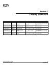
Ev10as150a-eb user guide 7-1 0977b–bdc–10/09 e2v semiconductors sas 2009 section 7 ordering information part number package temperature range screening comments ev10as150atp-eb ebga 317 ambient prototype for availability, contact your local e2v sales office. Ev10as150actp ebga 317 commercial grade t...
Page 38
Ordering information 7-2 ev10as150a-eb user guide 0977b–bdc–10/09 e2v semiconductors sas 2009.
Page 39: Section 8
Ev10as150a-eb user guide 8-1 0977b–bdc–10/09 e2v semiconductors sas 2009 section 8 appendix 8.1 ev10as150a-eb electrical schematics note: for adc decoupling strategy, please do not take into account the current decoupling implemented on current evaluation board which is purely experi- mental. Refer ...
Page 40
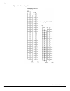
Appendix 8-2 ev10as150a-eb user guide 0977b–bdc–10/09 e2v semiconductors sas 2009 figure 8-1. Decoupling pin decoupling pin vccd decoupling pin v+d.
Page 41
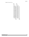
Appendix ev10as150a-eb user guide 8-3 0977b–bdc–10/09 e2v semiconductors sas 2009 figure 8-2. Decoupling pin v cca3.
Page 42
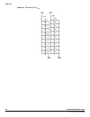
Appendix 8-4 ev10as150a-eb user guide 0977b–bdc–10/09 e2v semiconductors sas 2009 figure 8-3. Decoupling pin v cca5.
Page 43
Appendix ev10as150a-eb user guide 8-5 0977b–bdc–10/09 e2v semiconductors sas 2009 figure 8-4. Power supplies connections dg nd vcca3 vcca5 dgnd f2 0 e2 0 r1 7 m2 5 f2 2 d2 2 c2 2 c2 7 b2 7 a2 7 c2 6 a2 6 d1 4 t2 0 r2 0 d2 7 m2 7 b2 6 d2 6 l26 l25 c2 4 d2 4 r2 1 u2 1 l27 n2 7 k2 6 m2 6 n2 6 a2 5 b2 5...
Page 44
Appendix 8-6 ev10as150a-eb user guide 0977b–bdc–10/09 e2v semiconductors sas 2009 figure 8-5. Power supplies bypassing dgnd dgnd vcca3 v+d dgnd 3v3 dgnd vcca5 dgnd vccd dgnd dgnd dgnd dgnd dgnd 1 2 c2 1uf 1 2 j32 1 2 j41 1 2 c70 1uf 1 2 c6 1uf 1 2 c65 1uf 1 2 j42 1 2 c1 1uf 1 2 j45 1 2 j49 1 2 j20 1...
Page 45
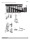
Appendix ev10as150a-eb user guide 8-7 0977b–bdc–10/09 e2v semiconductors sas 2009 figure 8-6. Ev10as150a-eb electrical schematic (adc dmux) drr sdat a sc lk r eset asyncrs t diode-ad c stag g sl dn bist rs drtype sl eep cl kdactr l asyncrs t drtyp e cl ktype bist rs sl eep stag g cl kdactr l dactrl ...
Page 46
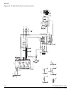
Appendix 8-8 ev10as150a-eb user guide 0977b–bdc–10/09 e2v semiconductors sas 2009 figure 8-7. Ev10as150a-eb electrical schematic (avr) sd at a sc l k sl d n r eset 3v 3 3v 3 3v 3 3v 3 3v 3 dg nd dg nd dg nd dg nd dg nd dg nd dgnd dg nd dg nd dg nd dg nd 3v 3 3v 3 3v 3 dg nd dg nd dg nd dg nd dg nd d...
Page 47
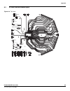
Appendix ev10as150a-eb user guide 8-9 0977b–bdc–10/09 e2v semiconductors sas 2009 8.2 ev10as150a-eb board layers figure 8-8. Top layer v+ d adc dgnd reset sc l k eval board adc ev10as15x series a 0 diode b9 b0 fc cl kdactrl clkn gnd d0 a o r /d r a n d 9 dor/ drdn a9 gn d cor/ drcn c9 drn dr (2 v 5 ...
Page 48
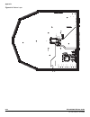
Appendix 8-10 ev10as150a-eb user guide 0977b–bdc–10/09 e2v semiconductors sas 2009 figure 8-9. Bottom layer 8.
Page 49
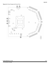
Appendix ev10as150a-eb user guide 8-11 0977b–bdc–10/09 e2v semiconductors sas 2009 figure 8-10. Board equipped with socket (top).
Page 50
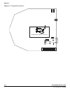
Appendix 8-12 ev10as150a-eb user guide 0977b–bdc–10/09 e2v semiconductors sas 2009 figure 8-11. Equipped board (bottom) r53 c 271 c277 c276 c8 7 c61 j4 1 j4 5 j2 3 j4 2 j3 2 c 1 2 0 c 1 9 6 c2 0 2 c 2 0 1 c2 0 0 c 1 9 9 j2 0 c 1 1 6 j2 6 c1 1 4 c 7 7 j4 9 j2 7 j3 0 j2 1 j2 2 c8 3 c 8 2 c7 1 c1 0 4 c...
Page 51
0977b–bdc–10/09 e2v semiconductors sas 2009 whilst e2v has taken care to ensure the accuracy of the information contained herein it accepts no responsibility for the consequences of any use thereof and also reserves the right to change the specification of goods without notice. E2v accepts no liabil...


