- DL manuals
- Echelon
- Transceiver
- LPT-11
- User Manual
Echelon LPT-11 User Manual
Summary of LPT-11
Page 1
L on w orks ® lpt-11 link power transceiver user’s guide version 1 @ echelon ® c o r p o r a t i o n 078-0198-01a.
Page 2
Echelon, lon, l on w orks , lonbuilder, nodebuilder, lontalk, lns, l on m ark , lonpoint, neuron, 3120, 3150, and the echelon logo are trademarks of echelon corporation registered in the united states and other countries. Lonsupport and lonmaker are trademarks of echelon corporation other brand and ...
Page 3: Contents
Contents 1 introduction 1-1 applications 1-3 audience 1-5 content 1-5 related documentation 1-6 2 electrical interface 2-1 lpt-11 pinout 2-2 network connection 2-4 clock input 2-4 neuron® chip communications port (cp) lines 2-4 pc board layout guidelines 2-4 choosing the inductor and capacitors for ...
Page 4
Iv contents 6 design issues 6-1 emi design issues 6-2 designing systems for emc (electromagnetic compatibility) 6-2 esd design issues 6-5 designing systems for esd immunity 6-5 surge design issues 6-6 designing systems for surge immunity 6-6 building entrance protection 6-7 en 61000-4 electromagnetc...
Page 5: Introduction
1 introduction the lpt-11 link power twisted pair transceiver provides a simple, cost effective method of adding a network-powered l on w orks transceiver to any neuron ® chip-based sensor, activator, display, lighting device, or general purpose i/o controller. The lpt-11 transceiver consists of a s...
Page 6
The lpt-11 transceiver supports free topology wiring, freeing the system installer from the need to wire in a doubly-terminated bus arrangement. Star, bus, and loop wiring are all supported by this architecture. Free topology wiring reduces the time and expense of system installation by allowing the...
Page 7: Applications
Applications a conventional control system using bus topology wiring (such as rs-485) consists of a network of sensors and control outputs that are interconnected using a shielded twisted pair wire. In accordance with eia rs-485 guidelines, all of the devices must be wired in a bus topology to limit...
Page 8
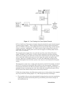
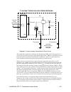
Figure 1.1 free topology link power system example lpt-11 link power transceivers located along the twisted wire pair include integral switching power supplies. These supplies regulate the voltage on the twisted pair down to +5vdc at currents up to 100ma for use by the neuron chip and the various se...
Page 9: Audience
2 if installers have been trained to use one style of wiring for all installations, free topology technology can be introduced without requiring retraining. 3. Retrofit installations with existing wiring plants can be accommodated with minimal rewiring, if any. This capability ensures that ft 3120 a...
Page 10: Related Documentation
1-6 introduction related documentation the following echelon documents are suggested reading: lonbuilder user's guide (078-0001-01) nodebuilder user's guide (078-0141-01) neuron c programmer's guide (078-0002-01) lonbuilder startup and hardware guide (078-0003-01) l on w orks lpi-10 link power inter...
Page 11: Electrical Interface
2 electrical interface the lpt-11 link power transceiver’s 14 pins provide a polarity insensitive connection to the twisted pair network, an interface to the neuron chip communications port, and a switching power supply. L on w orks lpt-11 transceiver user’s guide 2-1.
Page 12: Lpt-11 Pinout
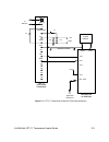
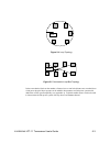
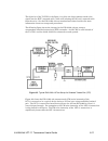
Lpt-11 pinout the pinout of the lpt-11 transceiver is shown in table 2.1. The interconnection between the lpt-11 and a neuron chip is shown in the block diagram in figure 2.1. See figure 3.1 for the physical location of pin 1. Table 2.1 lpt-11 transceiver pinout name pin# function net_a 1 connection...
Page 13
Net_a net_b v+ inductor vcc gnd clk nc txd rxd clk2 clk1 cp1 cp0 cp2 cp3 neuron 3120 or 3150 chip ground guard io0 - io10 to application electronics +5v clock circuit +5v c3 gnd c1 l1 c2 to network lpt-11 link power transceiver nc nc nc nc figure 2.1 lpt-11 transceiver-to-neuron chip interconnection...
Page 14: Network Connection
Network connection the network connection (net_a and net_b) is polarity insensitive, and therefore either of the two twisted pair wires can be connected to either of the two net pins. Details on network wiring are discussed in chapter 5. Transient protection may be required to protect the lpt-11 tra...
Page 15
Variations on this suggested pc board layout are possible as long as the general principles of grounding, shielding, guarding, and spacing are employed. For example, using a suitable fixture, the lpt-11 transceiver pins can be formed into a right angle before the transceiver is soldered onto the pc ...
Page 16
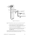
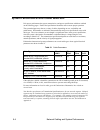
Figure 2.2 illustrates the connections between the lpt-11 transceiver and its four power supply-related components on one layer of a two-layer pc board. The other layer (generally the solder side of the board) should contain as much ground plane as possible. The switching power supply circuit in the...
Page 17: Switching Power Supply
In figure 2.2 are spaced as closely together as possible in order to minimize their loop area. Circuits that are sensitive to electric field noise should be kept away from l1 and pin 4 of the transceiver, and ground guarding should be employed to shield them from the electric field noise. The +5vdc ...
Page 18
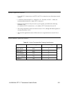
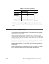
Table 2.3 examples of l1 inductor selections for consideration (1mh) manufacturer (series) part number temperature range taiyo-yuden (lhl08) lhl08-102j -40°c to +85°c * tdk (tsl) tsl0808-102kr26 -40°c to +85°c the inductors in table 2.3 are unshielded. For compact designs where the components are lo...
Page 19: Current Applications
Alternative inductor and capacitor selection for low- current applications for applications which require no more than 25ma dc of sustained current, such as a single physical layer repeater using an lpt-11 back-to-back with an ftt-10a, smaller, less-costly surface mount components for l1, c1, and c2...
Page 20
2-10 electrical interface.
Page 21: Mechanical Considerations
3 mechanical considerations this chapter discusses the mechanical footprint and connectors of the lpt-11 link power transceiver. Details of mounting the transceiver to an application electronics board containing a neuron chip are provided. L on w orks lpt-11 transceiver user’s guide 3-1.
Page 22: Mechanical Footprint
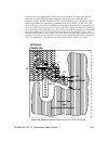
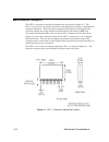
Mechanical footprint the lpt-11 transceiver mechanical dimensions are shown in figure 3.1. The lpt-11 transceiver is generally mounted to the application board as a through-hole, soldered component. Decisions about component placement on the application electronics board must also consider electroma...
Page 23: Power Output
4 power output this section describes the power supply portion of the lpt-11 link power transceiver, and provides suggestions for using the 5v output current. L on w orks lpt-11 transceiver user’s guide 4-1.
Page 24: Transceiver Output Power
Transceiver output power the lpt-11 transceiver power supply circuit performs a number of key functions: • draws dc power from the twisted pair network without interfering with communications with other devices; • regulates the output voltage (vcc) to +5vdc ±5% with a maximum steady state current of...
Page 25
Net_a net_b v+ inductor vcc gnd clk l1 c2 c1 +5v c3 ro lo co1 co2 to general circuitry lpt-11 to network to sensitive low-power analog circuits to higher-power resonant loads figure 4.1 post-filtering of vcc use the following guidelines to design the resistor and capacitor values for the r-c filter:...
Page 26
4-4 power output 1. Choose an lc product that sets the filter cutoff frequency at least a decade below the frequency of the resonant current demand (fd) in the load. That is, choose l o c o2 ≥ 100/(4π 2 f d 2 ); 2. L o must be large enough to keep the “effective capacitance” of c o2 as seen by the l...
Page 27: Network Cabling and
L on w orks lpt-11 transceiver user’s guide 5-1 5 network cabling and system performance this chapter provides information about cabling and network connections for the lpt-11 link power transceiver. This information includes a discussion of wire characteristics and power distribution issues..
Page 28: Network Overview
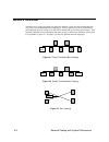
5-2 network cabling and system performance network overview the link power system is designed to support free topology wiring, and will accommodate bus, star, loop, or any combination of these topologies. Lpt-11 transceivers can be located at any point along the network wiring, as can the lpi-10 mod...
Page 29
L on w orks lpt-11 transceiver user’s guide 5-3 supply/ interface figure 5.4 loop topology supply/ interface figure 5.5 combination loop/bus topology in the event that the limits on the number of transceivers or total wire distance are exceeded, then a link power physical layer repeater can be added...
Page 30
5-4 network cabling and system performance system performance and cable selection link power performance has system, transmission, and power specifications which are outlined on the following pages. Each of the specifications should be met to ensure proper operation. The system designer may choose a...
Page 31
L on w orks lpt-11 transceiver user’s guide 5-5 system specifications • up to 128 lpt-11 transceivers or 64 ftt-10a/ft 31xx transceivers are allowed per network segment. • 1 link power unit load (lpul) = 25ma@vcc=5v. Therefore, 4 lpuls = 100ma, the recommended maximum for a single lpt-11 transceiver...
Page 32
5-6 network cabling and system performance table 5.3 free topology specifications the maximum total wire length is the total amount of wire connected per network segment. This means the sum of all wire lengths used, not simply the wire in the path between two devices. The maximum device-to-device di...
Page 33
L on w orks lpt-11 transceiver user’s guide 5-7 table 5.4 simplified power specifications using belden 85102 or belden 8471 (16awg/1.3mm) wire nominal worst case units 500 meter branch length, evenly distributed loading along a bus application current: 25 ma 128 128 devices 50 ma 64 64 100 ma 32 32 ...
Page 34
5-8 network cabling and system performance table 5.6 simplified power specifications using level 4/22awg (0.65mm) wire nominal worst case units 400 meter branch length, evenly distributed loading along a bus application current: 25 ma 74 53 devices 50 ma 37 26 100 ma 18 13 400 meter branch length, l...
Page 35
L on w orks lpt-11 transceiver user’s guide 5-9 i is the average application current of a device. The distance of an lpt-11 transceiver from the lpi-10 module is the device distance, d . For each branch, the sum of the products of a device distance and the application current of that device must not...
Page 36
5-10 network cabling and system performance in the following example, there are only two branches to check. Assume wire type is jy (st) y 2x2x0.8 and average wire temperature is 25°c. Thus, α = 1. Lpi-10 50m 50m 50m 20m 80m 50m 20m 2 devices 100ma each 100ma each 5 devices 5 devices 3 devices 100ma ...
Page 37
L on w orks lpt-11 transceiver user’s guide 5-11 example network 1, below, illustrates the simplification process in three steps. Distances are drawn in relative proportion. The numbers represent +5v application currents, with 5x25 indicating 5 devices of 25ma each at the same location. Use the equi...
Page 38
5-12 network cabling and system performance here is a second example that illustrates the benefits of the extended performance specification and the importance of the sub-branching simplification procedure. Without simplifying the network, the sample topology fails to meet the power specification. H...
Page 39: Cable Termination
L on w orks lpt-11 transceiver user’s guide 5-13 cable termination a link power network segment requires termination for proper data transmission performance. A total termination impedance of approximately 52Ω is required. Free topology segment in a free topology segment, only one termination is req...
Page 40
5-14 network cabling and system performance.
Page 41: Design Issues
6 design issues this chapter looks at design issues, and includes discussions of electromagnetic interference (emi), electrostatic discharge (esd), and surge for the lpt-11 link power transceiver. L on w orks lpt-11 transceiver user’s guide 6-1.
Page 42: Emi Design Issues
Emi design issues the high-speed digital signals associated with microcontroller designs can generate unintentional electromagnetic interference (emi). High-speed voltage transitions generate rf currents that can cause radiation from a product if a length of wire or piece of metal can serve as an an...
Page 43
Twisted pair network leakage capacitances to earth ground c leak,gnd c load lpt-11 v cc node logic ground "floating" device on link power network c decouple c leak,signal v gate net_a net_b vcc gnd figure 6.1 parasitic leakage capacitances to earth ground the single most important technique for desi...
Page 44
For example, in most link power devices that use the neuron 3120 chip, the only fast digital signal that needs to be routed across the pc board is the clk2 line from the neuron chip to the lpt-11 transceiver (clk on transceiver pin 7, see figure 2.1). If a two-layer pc board is being used, clk2 can ...
Page 45: Esd Design Issues
• a common-mode ferrite choke can be used to help meet emc requirements for devices that have noisy application circuitry or special circuit requirements. Note that it may be possible to design a two-layer 10mhz neuron 3150 chip-based link power device that will pass level “b” in some applications, ...
Page 46: Surge Design Issues
Connector. If metal must be accessible on the outside of a device’s enclosure, then it may be necessary to provide an earth ground connection to that metal. For example, if metal toggle switches must be user-accessible, then it may be necessary to mount the switches on a metal plate that is earth gr...
Page 47: Building Entrance Protection
Tvs devices used with lpt-11 transceivers must meet the following requirements: • bi-directional protection; • rated at 400w minimum peak power (10/1000µs waveform) rating; • working peak reverse voltage rating vrwm ≥ 42.4v (-40°c to +85°c); vrwm should be as low as possible over the temperature ran...
Page 48
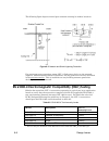
The following figure depicts twisted pair networks running in outdoor locations. Figure 6.3 network and shield lightning protection for maximum surge protection, every lpt-11 link power device on the network segment, whether located indoors or outdoors, has the protection circuitry described in the ...
Page 49
En 61000-4-2 esd testing is performed on a metal test table using an esd transient generator. Level 4 testing involves injecting up to ±8kv contact discharges and up to ±15kv air discharges into the product under test. Depending on the product design, discharges may be injected at the network connec...
Page 50
The 80% am). Level 3 testing, which represents a “harsh industrial environment,” is performed with an injected common-mode voltage on the eut’s network cable of 10vrms (50.9vp-p including the 80% am). Note that the cdn test method is the preferred method according to the en 61000- 4-6 specification....
Page 51
The objective of the t2 cdn in the figure is to drive the large common-mode noise signal into the eut’s network cable, while still isolating the ae unit’s network cable from the noise. See the en 61000-4-6 test standard and related articles for more information about test setups and procedures. The ...
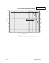
Page 52
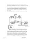
Lpt-11 transceiver common mode noise immunity 0.00 2.00 4.00 6.00 8.00 10.00 12.00 14.00 16.00 100000.00 1000000.00 10000000.00 100000000.00 frequency (hz) amplit ude ( v rm s) 0.00 5.00 10.00 15.00 20.00 25.00 30.00 35.00 40.00 45.00 50.00 55.00 60.00 65.00 70.00 75.00 80.00 amplit ude ( vp- p) lpt...
Page 53: Programming Considerations
7 programming considerations this section explains the integration of the lpt-11 link power transceiver using the lonbuilder developer’s workbench and nodebuilder development tool. It covers considerations relating to channel definition and custom device image generation. L on w orks lpt-11 transcei...
Page 54
Application program development and export applications are initially developed, tested, and debugged using the lonbuilder developer’s kit or the nodebuilder development tool. See the lonbuilder user’s guide or the nodebuilder user’s guide for detailed instructions on developing and testing applicat...
Page 55
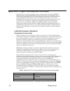
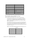
Osc accuracy 200ppm osc wakeup 0µsec avg packet size 15 bytes collision detect no cd terminate after preamble no cd through packet end no bit sync threshold 4.0 bits rcv start delay 9.0 bits (see notes 1 and 2) rcv end delay 0.0 bits indeterm time 24.0 bits min interpacket time 0.0 bits turnaround 0...
Page 56
The final step in the process is the selection of a target hardware platform. In the development phase, a lonbuilder emulator is used. To select this target hardware, click the app node button and then the target hw button from the lonbuilder navigator. Create a target hardware template that uses em...
Page 57: Nodebuilder Development Tool
Nodebuilder development tool the nodebuilder development tool, release 3 and newer, manages two application and target hardware configurations for each project. One is the development target and the other is the release target. Development targets are used during development; release targets are use...
Page 58
7-6 design issues 4 for flash memory parts, specify the sector size. For eeprom memory, set the write time. A list of echelon tested external memory components can be found on the echelon website at www.Echelon.Com. Once the hardware template has been created, drag the new hardware template to the r...
Page 59: References
8 references this section provides a list of the reference material used in the preparation of this manual. L on w orks lpt-11 transceiver user’s guide 8-1.
Page 60: Reference Documentation
8-2 references reference documentation the documentation used in this manual was from the following sources. Echelon documents l on w orks lpi-10 link power interface module user's guide, echelon corporation, part number 078-0104-01. Toshiba tmpn3150 neuron chip data book, part number bpl9 99 805. L...
Page 61: Appendix A
L on w orks lpt-11 transceiver user’s guide a-1 appendix a physical layer repeaters this section explains the physical layer repeater function of the lpt-11 transceiver..
Page 62: Physical Layer Repeaters
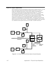
A-2 appendix a – physical layer repeaters physical layer repeaters each link power transceiver incorporates a physical layer repeater function. If a link power system grows beyond the maximum number of transceivers or total wire length, then additional link power systems can be added by interconnect...
Page 63
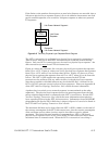
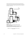
L on w orks lpt-11 transceiver user’s guide a-3 if the limits on the number of transceivers or total wire distance are exceeded, then a link power physical layer repeater (figure a.2) can be added to interconnect two link power network segments, or to connect a link power segment to other non-powere...
Page 64
A-4 appendix a – physical layer repeaters packet, all of the ftt-10a transceivers in the physical layer repeater will be in transmit mode, repeating the packet onto their respective segments. Therefore, in a 5-way physical layer repeater, the maximum current consumption when the lpt-11 transceiver i...
Page 65
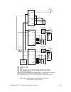
L on w orks lpt-11 transceiver user’s guide a-5 5mhz clock oscillator n-input or ub net_a net_b t1 txd ftt-10a +5v c1b c4b c3b d2b d1b c5b r1b r2b net1 net2 pcb spark gaps net_a net_b +5v c1n c4n c3n d2n d1n c5n r1n r2n net1 net2 pcb spark gaps un see text in ftt-10a user guide. Network segment b ne...
Page 66
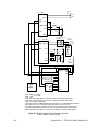
A-6 appendix a – physical layer repeaters 5mhz clock oscillator ua ub net_a net_b vcc v+ gnd txd rxd clk lpt-11 +5v c1 l1 net1 net2 net_a net_b t1 ftt-10a +5v c1b see text in ftt-10a user guide. C4b c3b d2b d1b c5b r1b r2b net1 net2 pcb spark gaps q6 q7 q10 q11 q12 >clk rst i0/clk i1 i2 i3 i4 i5 i6 ...
Page 67: Appendix B
Appendix b differences between lpt-10 and lpt-11 this appendix contains information on differences in design from the lpt-10 to the lpt-11 transceiver. L on w orks lpt-11 transceiver user’s guide b-1.
Page 68: Transceivers
Differences between lpt-10 and lpt-11 link power transceivers the following sections discuss the functional differences between the lpt-10 and lpt-11 transceivers, as well as differences in form, plus address the modifications required for migrating from the lpt-10 to the lpt-11. Functional differen...
Page 69: Transceiver
• in the lpt-10 transceiver the clksel0 and the clksel1 pins are used to select the frequency of the input clock. The new lpt-11 transceiver design has an auto clock select feature and does not require the functionality previously provided by the clksel0 and the clksel1 pins. • pin #11 txen becomes ...
Page 70
B-4 appendix b - differences between lpt-10 and lpt-11.
Page 71: Appendix C
Appendix c lpt-11 transceiver-based device checklist this appendix includes a checklist to ensure that products using the lpt-11 transceiver meet the specifications presented in this user’s guide. L on w orks lpt-11 transceiver user’s guide c-1.
Page 72
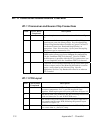
Lpt-11 transceiver-based device checklist lpt-11 transceiver and neuron chip connections item check when completed description 1 transceiver pins connected as shown in table 2.1 and figure 2.1 2 the recommended number and placement of 0.1µf bypass capacitors are near the neuron chip. See the appropr...
Page 73
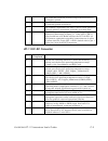
9 the clk2 trace from the neuron chip to the transceiver is guarded by ground. 10 the lpt-11 device's logic ground is electrically floating from all external ground connections. 11 the “leakage” capacitance the lpt-11 device's logic ground to external ground is minimized, preferably less than 10pf. ...
Page 74
Lpt-11 transient immunity item check when completed description 21 if 1.0kv or 2.0kv surge immunity is desired, an appropriate tvs device from table 6.1 is placed differentially across net_a and net_b. For 0.5kv surge immunity, no tvs should be needed. 22 the device's package is designed to prevent ...
Page 75
29 if the network configuration is doubly-terminated bus, one lpi-10 source coupler is placed at one end of the bus to provide power and one termination (with its termination jumper in the “2cplr” setting), plus a standard 105Ω tp/ft termination is placed the other end of the dt bus (see figure 5.6....
Page 76
C-6 appendix c - checklist.

