Fairchild SEMICONDUCTOR RC5050 Application Note
Application Note 50
Implementing the RC5050 and RC5051 DC-DC
Converters on Pentium
®
Pro Motherboards
www.fairchildsemi.com
Introduction
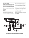
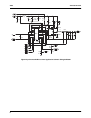
This document describes how to implement a switching volt-
age regulator using an RC5050 or an RC5051 high speed
controller, a power inductor, a Schottky diode, appropriate
capacitors, and external power MOSFETs. This regulator
forms a step down DC-DC converter that can deliver up to
14.5A of continuous load current at voltages ranging from
1.3V to 3.5V. A specific application circuit, design consider-
ations, component selection, PCB layout guidelines, and per-
formance evaluations are covered in detail.
In the past 10 years, microprocessors have evolved at such an
exponential rate that a modern chip can rival the computing
power of a mainframe computer. Such evolution has been
possible because of the increasing numbers of transistors that
processors integrate. Pentium CPUs, for example, integrate
well over 5 million transistors on a single piece of silicon.
To integrate so many transistors on a piece of silicon, their
physical geometry has been reduced to the sub-micron level.
As a result of each geometry reduction, the corresponding
operational voltage for each transistor has also been reduced.
The changing CPU voltage demands the design of a pro-
grammable power supply—a design that is not completely
re-engineered with every change in CPU voltage.
The voltage range of the CPU has shown a downwards trend
for the past 5 years: from 3.3V for the Pentium, to 3.1V for
the Pentium Pro, and to 1.8V for future processors. With this
trend in mind, Raytheon Electronics has designed the
RC5050 and RC5051 controllers. These controllers integrate
the necessary programmability to address the changing
power supply requirements of lower voltage CPUs.
Previous generations of DC-DC converter controllers were
designed with fixed output voltages adjustable only with a
set of external resistors. In a high volume production envi-
ronment (such as with personal computers), however, a CPU
voltage change requires a CPU board re-design to accommo-
date the new voltage requirement. The 5-bit DAC in the
RC5050 and the RC5051 reads the voltage ID code that is
programmed into modern processors and provides the appro-
priate CPU voltage. In this manner, the PC board does not
have to be re-designed each time the CPU voltage changes.
The CPU can thus automatically configure its own required
supply voltage.
Intel Pentium Pro Processor Power
Requirements
Refer to Intel’s AP-523 Application Note, Pentium
®
Pro
Processor Power Distribution Guidelines, November 1995
(order number 242764-001), as a basic reference. The speci-
fications contained in this document have been modified
slightly from the original Intel document to include updated
specifications for more recent processors. Please contact
Intel Corporation for specific details.
Input Voltages
Available inputs are +12V
±
5% and +5V
±
5%. Either one or
both of these inputs can be used by the DC-DC converter.
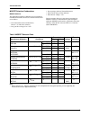
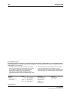
The input voltage requirements for Raytheon’s RC5050
and RC5051 DC-DC converters are listed in Table 1.
Table 1. Input Voltage Requirements
Pentium Pro DC Power Requirements
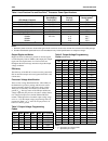
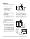
Refer to Table 2, Intel Pentium Pro and OverDrive
®
Proces-
sor Power Specifications. For a motherboard designs without
a standard VRM (Voltage Regulator Module) socket, the
on-board DC-DC converter must supply a minimum of
13.9A of current @2.5V and 12.4A of current @3.3V. For a
Flexible Motherboard design, the on-board DC-DC con-
verter must supply 14.5A maximum I
CC
P.
DC Voltage Regulation
As indicated in Table 2, the voltage level supplied to the
CPU must be within
±
5% of its nominal setting. Voltage reg-
ulation limits must include:
• Output load ranges specified in Table 2
• Output ripple/noise
• DC output initial voltage set point
• Temperature and warm up drift (Ambient +10
°
C to +50
°
C
at full load with a maximum rate of change of 5
°
C per 10
minutes minimum but no more than 10
°
C per hour)
• Output load transient with:
Slew rate >30A/
µ
s at converter pins
Range: 0.3A - I
CC
P Max (as defined in Table 2).
Part #
Vcc for IC
MOSFET
Drain
MOSFET
Gate Bias
RC5050
RC5051
+5V
±
5%
+5V
±
5%
12V
±
5% or
+5V
±
5%
Rev. 1.1.0

