- DL manuals
- Icom
- Transceiver
- IC-4088E
- Service Manual
Icom IC-4088E Service Manual
Summary of IC-4088E
Page 1
Service manual lpd fm transceiver 1-1-32, kamiminami, hirano-ku, osaka, 547-0003, japan s-13910iz-c1 printed in japan © 2002 by icom inc..
Page 2
Introduction danger ordering parts repair notes this service manual describes the latest service information for the ic-4088e lpd fm transceiver at the time of pub- lication. Never connect the transceiver to an ac outlet or to a dc power supply that uses more than 5.0 v. Such a connection could caus...
Page 3
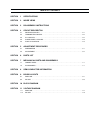
Table of contents section 1 specifications section 2 inside views section 3 disassembly instructions section 4 circuit descripiton 4-1 receiver circuits . . . . . . . . . . . . . . . . . . . . . . . . . . . . . . . . . . . . . . . . . . . . . . . . . . . . .4-1 4-2 transmit t er circuits . . . . . ....
Page 4: Section 1
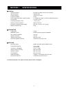
Section 1 specifications 1 - 1 ‘ ‘ general • number of channel : 69 channels (simplex; 433.075–434.775 mhz) • type of emission : 16k0f3e (fm) • freqency stability : ±2500 hz (±5.7 ppm) • freqency resolution : 25 khz • power supply requirement (negative ground) : 3 × aa (r6) dry, alkaline; or bp-202 ...
Page 5
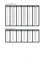
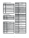
1 - 2 channel frequency list ctcss frequency list 1 2 3 4 5 6 7 8 9 10 11 12 13 14 15 16 17 18 19 20 21 22 23 433.0750 433.1000 433.1250 433.1500 433.1750 433.2000 433.2250 433.2500 433.2750 433.3000 433.3250 433.3500 433.3750 433.4000 433.4250 433.4500 433.4750 433.5000 433.5250 433.5500 433.5750 4...
Page 6: Section 2
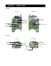
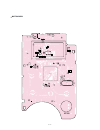
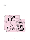
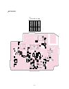
Section 2 inside views • main unit 2 - 1 • rf unit r+3 regulator (q304: 2sa1586) +3 regulator (ic303: r1121n301b) eeprom (ic300: br24c02) cpu (ic301: µ pd78f9418agk) audio amplifier (ic305: njm2070) t+3 regulator (q308: 2sb798) top view bottom view 1st mixer (q2: 2sc4226) pll ic (ic2: tb31202fn) 2nd...
Page 7: Section 3
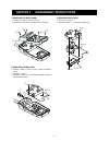
Section 3 disassembly instructions 3 - 1 rear panel b a b c d f g main unit e rf unit main unit i h • removing the rear panel 1 unscrew 1 screw a , and 5 screws b . 2 remove the rear panel in the direction of the arrow. • removing the rf unit 1 unscrew 2 screws h . 2 unsolder 2 points i , and remove...
Page 8: Section 4
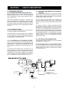
4 - 1 section 4 circuit description 4-1 receiver circuits 4-1-1 antenna switching circuit (rf unit) received signals from the antenna connector are passed through the low-pass filter (l1–l3, c1–c5). The filtered sig- nals are applied to the λ ⁄ 4 type antenna switching circuit (d1 -d4, l5, l6, c9, c...
Page 9
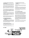
4 - 2 4-1-6 squelch circuit (rf and main units) (1) noise squelch the noise squelch circuit cuts out af signals when no rf signals are received. By detecting noise components in the af signals, the squelch circuit switches the af mute switch. A portion of the af signals from the fm if ic (rf unit; i...
Page 10
Input port for the pll unlock signal from the pll ic (rf unit; ic2). Low : during unlock. Input port for the ptt switch from the external mic jack (main unit; j303). Low : external ptt switch is on. Input port for the control signal from the external remote microphone. Input port for the transceiver...
Page 11: Section 5
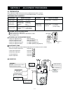
Test j1 to rf unit j1 dc power supply 4.5 v /1.0 a frequency counter fm deviation meter caution: do not transmit while the ssg is connected to the antenna. Rf power meter 50 Ω / 1–500 mw to sp jack hm-75a to mic jack audio generator ac millivoltmeter to dc in standard signal generator connection ent...
Page 12
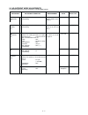
5 - 2 reference frequency [fr] output power [pl] fm deviation [dl] ctcss [to] squelch [sq] 433.925000 mhz 10 mw ±4.1 khz ±0.70 khz audio signal disappears. • operating channel : ch 35 • transmitting • operating channel : ch 35 • transmitting • operating channel : ch 35 • connect an audio generator t...
Page 13
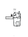
5 - 3 test j1 rf gnd j1 rf test port entering the adjustment mode q turn the transceiver power off. W while connecting the "test" to gnd, then turn power on..
Page 14: Section 6
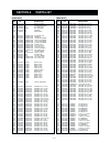
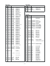
[main unit] [main unit] ic300 1130011230 s.Ic br24c02fv-we2 ic301 1140011170 s.Ic µpd78f9418agk-9eu ic302 1110005820 s.Ic r3112n281a-tr ic303 1180002430 s.Reg r1121n301b-tr ic304 1130007382 s.Ic ak2342b ic305 1110002810 s.Ic njm2070m-t1 q302 1590001330 s.Transistor dta114eua t106 q303 1590002490 s.T...
Page 15
C329 4030017420 s.Ceramic ecj0ec1h470j c330 4030016930 s.Ceramic ecj0eb1a104k c331 4030016930 s.Ceramic ecj0eb1a104k c332 4030017460 s.Ceramic ecj0eb1e102k c333 4030017730 s.Ceramic ecj0eb1e471k c334 4030016930 s.Ceramic ecj0eb1a104k c335 4030017440 s.Ceramic ecj0ec1h221j c336 4030017430 s.Ceramic e...
Page 16
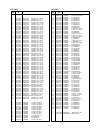
S.=surface mount [rf unit] [rf unit] l24 6200005630 s.Coil eljre 5n6z-f r1 7030005060 s.Resistor erj2gej 333 x (33 k Ω ) r2 7030007260 s.Resistor erj2gej 330 x (33 Ω ) r3 7030004970 s.Resistor erj2gej 470 x (47 Ω ) r4 7030005090 s.Resistor erj2gej 104 x (100 k Ω ) r5 7030005040 s.Resistor erj2gej 47...
Page 17
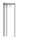
[rf unit] w4 7030010040 s.Jumper erj2ge-jpw w5 7030010040 s.Jumper erj2ge-jpw w6 7030010040 s.Jumper erj2ge-jpw w8 7030010040 s.Jumper erj2ge-jpw w9 7030010040 s.Jumper erj2ge-jpw ep2 6910013310 s.Bead mmz1608d121b ep3 0910055942 pcb b-5919b 6 - 4 ref order description no. No. S.=surface mount.
Page 18: Section 7
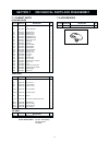
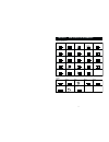
Section 7 mechanical parts and disassembly 7 - 1 screw abbreviations b0, bt: self-tapping ph: pan head zk: black sp1 2510001120 speaker sdrs-3650p-008 1 ep1 3310003060 antenna 2628 ant 1 mp1 8210019410 2628 front panel 1 mp2 8110007920 2628 rear cover 1 mp3 8210019420 2628 rear panel 1 mp4 831005474...
Page 19
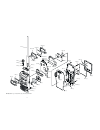
7 - 2 unit abbreviation (c): chassis parts, (rf): rf unit, (m): main unit ep1 (c) mp15 (c) mp16 (c) mp25 (c) mp7 (c) mp6 (c) mp8 (c) mp4 (c) mp3 (c) mp36 (c) mp33 (c) mp32 (c) mp32 (c) mp20 (c) mp2 (c) mp14 (c) mp12 (c) mp302 (m) mp303 (m) ep303 (m) ds300 (m) mp301 (m) main unit rf unit mp1 (c) sp1 ...
Page 20
Section 8 semi-conductor information 8 - 1 • diodes • transistor and fet’s 2sa1362 gr (symbol: aeg) 2sc4213 b (symbol: ab) 2sc5108 y (symbol: mc) dta114 eu (symbol: 16) dtc114tu (symbol: 04) umz2n (symbol: z2) 2sc5194 (symbol: t88) 2sj144gr (symbol: vg) 2sj144 y (symbol: vy) 2sk1829 (symbol: k1) dtc...
Page 21: Section 9
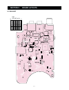
Section 9 board layouts 9-1 main unit 9 - 1 c377 j303 test cl s305 j302 b5918d sp sp + j301 r406 s304 j300 c354 c364 j300 c347 r377 r381 r363 r357 r373 c344 c335 c339 ic304 r378 c346 r384 r392 c361 r374 r366 r358 c389 c334 r356 r348 r346 c336 r359 r344 c329 c332 r361 r365 r388 c351 q313 c348 c328 q3...
Page 22
9 - 2 • bottom view r405 r404 c374 c341 r349 c368 r410 c350 r414 c383 r304 c311 r364 ep300 x300 c303 ep301 ep302 q308 w304 r369 c325 c321 c316 w307 r340 r333 r334 ic301 sp sp + mc300 r335 r338 r327 c313 c326 d303 d304 c352 r421 r350 c338 r343 ds301 c365 r413 r412 c300 c301 r305 r424 c388 c387 c386 c...
Page 23
9 - 3 9-2 rf unit • top view r65 c88 c16 c15 l7 c14 c12 c11 d4 l6 d2 c10 c9 l5 r2 r1 d3 q1 r3 l24 fi1 c39 c75 c49 c44 r32 r31 r27 c43 c42 r26 r29 r33 c46 c47 r45 c69 d12 c91 r79 r86 r49 d11 r51 r48 c76 d10 r87 c77 r50 c92 r66 c102 r80 r69 r67 r70 c54 r36 c74 c50 r39 c55 l21 d9 l23 c56 c52 c51 c60 c1...
Page 24
9 - 4 • bottom view c72 c61 c66 r25 d7 d6 c37 c65 w6 c40 w5 r44 r43 c64 c67 c41 r24 r23 r22 r21 r46 c62 c17 r5 c103 r20 c34 c13 l8 c99 r7 c28 d1 c2 c8 l4 c3 l3 c4 c1 l1 c5 l2 w8 r8 c23 c86 r64 c87 r34 c45 ic1 r9 r10 c48 c24 q3 l12 c26 r11 l10 c25 c6 c7 l11 c27 r14 c29 q4 r4 r77 c22 w9 l9 r6 c21 j2 q...
Page 25
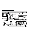
Section 10 block diagram 10 - 1 antenna lpf hpf tx/rx sw rf amp bpf bpf xtal if amp if amp bpf ceramic x1 cdbc450cx24 noise det buff att drive amp pwr amp mc300 kuc3523 ptt s304 up s300 down s301 mode s302 power s303 j303 j302 dc 6v in j301 x300: cr-465 af amp af mute +3 reg lcd sp300 sdrd-3650p rv-...
Page 26
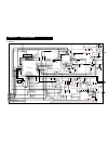
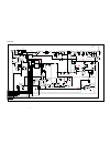
Section 11 voltage diagram 11 - 1 11-1 main unit *: ext-ptt t: 2.30 r: 3.10 t+3 [bp] dc.In ext.Sp mic ext-dc: 0.32 chg: 2.99 t: 2.09 r: 0.00 t: 2.99 r: 0.00 t: 0.00 r: 0.00 c: 2.99 c: 3.10 t: 0.00 r: 2.73 t: 0.00 r: 1.91 ext-dc: 5.98 ext-dc: 5.73 bp: 4.50 t: 0.00 r (bp): 4.50 r (ext-dc): 5.73 *: at ...
Page 27
11-2 rf unit 11 - 2 antenna cpa l2 17 nh l3 17 nh c2 6 p c7 7 p l4 27 nh c9 6 p l5 18 nh l6 12 nh c10 7 p c11 0.01 r1 33 k r2 33 r3 47 c14 10 p c16 10 p c17 1 p c19 470 p c21 22 p c22 10 p r4 100 k r6 1.2 k r7 470 l8 27 nh r8 1.5 k r9 82 k r10 820 q3 2sc4215 0 l10 0.82 h r11 220 c26 9 p c27 8 p c30 ...
Page 28
Introduction danger ordering parts repair notes this service manual describes the latest service information for the ic-4088e lpd fm transceiver at the time of pub- lication. Never connect the transceiver to an ac outlet or to a dc power supply that uses more than 5.0 v. Such a connection could caus...
Page 29: Service
Service manual lpd fm transceiver 1-1-32, kamiminami, hirano-ku, osaka, 547-0003, japan s-13910iz-c1 © 2002 icom inc..

