- DL manuals
- Icom
- Two-Way Radio
- IC-718
- Service Manual
Icom IC-718 Service Manual
Summary of IC-718
Page 1
S-13701mz-c1 © 2000 icom inc. 6-9-16, kamihigashi, hirano-ku, osaka 547-0002, japan count on us! Hf tranceiver ic-718 ic-718.
Page 2
Repair notes 1. Make sure a problem is internal before disassembling the transceiver. 2. Do not open the transceiver until the transceiver is disconnected from its power source. 3. Do not force any of the variable components. Turn them slowly and smoothly. 4. Do not short any circuits or electronic ...
Page 3
Table of contents section 1 specifications section 2 inside views section 3 disassembly instructions section 4 circuit description 4 – 1 receiver circuits ................................................................................................................... 4 – 1 4 – 2 transmitter circu...
Page 4: Section 1
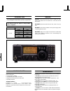
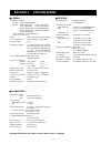
Section 1 specifications 1 - 1 ■ general • frequency coverage : receive 0.030–29.999999 mhz* 1 transmit 1.800–1.999 mhz* 2 3.500–3.999 mhz* 2 7.000–7.300 mhz 10.100–10.150 mhz 14.000–14.350 mhz 18.068–18.168 mhz 21.000–21.450 mhz 24.890–24.990 mhz 28.000–29.700 mhz * 1 guaranteed range: 0.5–29.99999...
Page 5: Section 2
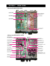
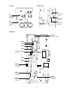
2 - 1 section 2 inside views filter unit pa unit main unit pll unit ¡ top view (pa and filter units) ¡ bottom view (main and pll units) rx rf preamplifier (q1401, q1402: 2sk2171) tx mixer (q101, q102: 3sk131) 1st lo amplifier (q201: 2sc4673) rx 1st mixer circuit (64.455 mhz) dds gate allay ic (ic6: ...
Page 6: Section 3
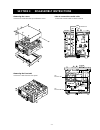
3 - 1 section 3 disassembly instructions • removing the covers remove 14 screws from the top and bottom covers. • removing the front unit remove 4 screws from the front panel. • how to connect the coaxial cable connect the coaxial cable as shown in below. J6 j3 to main unit pa unit filter unit j1 j7...
Page 7: Section 4
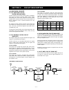
Section 4 circuit description 4 - 1 4-1 receiver circuits 4-1-1 rf switching circuit (filter and main units) the rf switching circuit leads receive signals to bandpass filters from the antenna connector while receiving. While transmitting, this circuit leads signals from the rf power amplifier to th...
Page 8
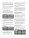
4 - 2 the signals from the pre-amplifier circuit, or signals which bypass the pre-amplifier, pass through a low-pass filter (l902, l903, c902–c907). This low-pass filter suppresses signals above 30 mhz to eliminate direct receiving of signals at 64.455 mhz and image interference at 130–160 mhz. The ...
Page 9
4 - 3 4-1-10 ssb/cw demodulator circuits (main unit) in ssb or cw mode, the 2nd if signal from the if amplifier (q1601) is mixed with the bfo signal from the pll unit at the product detector (ic2001) to demodulate the 2nd if sig- nal into af signals. The detected signals (af) from ic2001 (pin 1) are...
Page 10
4 - 4 4-2 transmitter circuits 4-2-1 microphone amplifier circuit (front and main units) the microphone amplifier circuit amplifies microphone-input signals and outputs the amplified signal to the balanced modulator. Audio signals from the [mic] connector are applied to the mic amplifier ic (ic2201)...
Page 11
4 - 5 when the “for” voltage exceeds the “pocv” voltage, alc bias voltage from ic1701c (pin 8) controls the if amplifiers (q151, q502). This adjusts the output power to the deter- mined level by the rf power setting until the “for” and “pocv” voltages are equalized. In am mode, q1705 turns on and c1...
Page 12
4 - 6 4-3-3 reference oscillator circuit (pll unit) the reference oscillator circuit consists of q9 and x1. A 32.00 mhz reference frequency is oscillated to produce a 2nd lo signal, dds reference frequency and bfo dds clock signal. The 32.00 mhz reference frequency is doubled at q10 to obtain the 2n...
Page 13
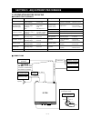
Section 5 adjustment procedures 5 - 1 5-1 preparation before servicing ■ required test equipment dc power supply rf power meter (terminated type) frequency counter rf voltmeter modulation analyzer distortion meter oscilloscope digital multimeter spectram analyzer standard signal generator (ssg) ac m...
Page 14
5 - 2 5-2 pll adjustments reference frequency vco lock voltage 1st lo output level 2nd lo output level bfo output adjustment adjustment adjustment condition measurement value point unit location unit adjust 1 2 3 1 2 1 2 1 1 2 3 • display frequency: any • set c16 as illustration at below. • receivin...
Page 15
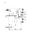
5 - 3 2nd lo j1 1 2 1 2 p2 bfo j2 1 2 1st lo j4 1 2 1 2 p3 c7 c6 reference osc level adjustment p1 reference frequency check point c16 reference frequency pre-setting p4 1st lo output level check point p5 bfo check point c165 vco lock voltage adjustment l4 reference freauency adjustment • pll unit.
Page 16
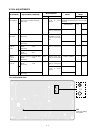
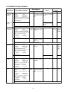
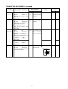
5 - 4 5-3 transmitter adjustments idling current (for driver) (for final amplifier) swr detector transmitter total gain output power ic apc adjustment adjustment adjustment condition measurement value point unit location unit adjust 1 2 1 2 1 2 1 1 • display frequency: 14.10000 mhz • mode : usb • rf...
Page 17
5 - 5 cp4002 ic apc pre-setting j3601 idling current pre-setting r1707 output power adjustment l151 tx total gain adjustment l106 r503 l501 l303 l302 l301 r1720 ic apc adjustment r2701 tx total gain pre-setting r21 idling current adjustment (driver) r24 idling current adjustment (final) j5 swr detec...
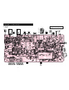
Page 18
5 - 6 transmitter adjustments—continued carrier suppression am carrier am modulation cw carrier adjustment adjustment adjustment condition measurement value point unit location unit adjust 1 1 1 2 1 • display frequency: 14.10000 mhz • mode : usb • mic gain : minimum (0) • apply no audio signals to [...
Page 19
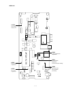
5 - 7 cp3701 cw carrier check point r3703 cw carrier adjustment r1730 am carrier adjustment r2321 am modulation adjustment (or am carrier pre-setting) r2385 am carrier and am modulation pre-setting r2303 carrier suppression adjustment • main unit.
Page 20
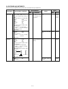
5 - 8 *this output level of a standard signal generator (ssg) is indicated as ssg’s open circuit. 5-4 receiver adjustments receiver total gain adjustment must perform after transmitter total gain adjustment. Receiver total gain noise blanker adjustment adjustment adjustment condition measurement val...
Page 21
5 - 9 l1621 l1614 rx total gain adjustment l1103 l1202 l1201 r2701 rx total gain pre-setting l1501 cp1501 noise blanker check point l1502 noise blanker adjustment • main unit.
Page 22
5 - 10 5-5 set mode adjustment entering set mode adjustment for rx volume center s meter set mode adjustment for tx filter calibration power meter alc meter adjustment adjustment condition display operation • enter set mode adjustment for rx: 1 turn power off. 2 terminate the [remote] jack with a 3....
Page 23
5 - 11 set mode adjustment —continued swr meter adjustment adjustment condition display operation • connect a 50 Ω dummy load or power meter to [ant] connector. • connect a 100 Ω dummy load or power meter to [ant] connector. 1 2 transmit using an external ptt switch to set swr reference level after ...
Page 24: Section 6 Parts List
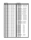
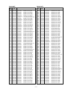
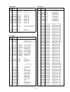
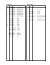
S.=surface mount sp1 2510000670 speaker vs-50-0827 w3 8900008930 cable opc-885 w4 8900008930 cable opc-885 w5 8900006990 cable opc-683 ws1 8970023640 e.Other sx2242 icom shield (1)/fr ep1 6910012480 e.Other rms20-250-201-1r ep2 6450001230 e.Other hlj0999-01-480 ic1 1140009160 s.Ic hd6433837sd17h ic2...
Page 25
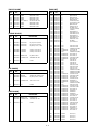
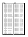
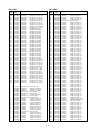
[logic board] [logic board] s.=surface mount r59 7030003560 s.Resistor erj3geyj 103 v (10 k Ω ) r62 7030003480 s.Resistor erj3geyj 222 v (2.2 k Ω ) r63 7030003480 s.Resistor erj3geyj 222 v (2.2 k Ω ) r70 7030003370 s.Resistor erj3geyj 271 v (270 Ω ) r71 7030003410 s.Resistor erj3geyj 561 v (560 Ω ) ...
Page 26
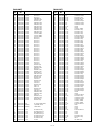
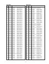
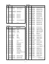
[main unit] [logic board] s.=surface mount ep1 0910052055 pcb b 5382e ep2 6910012350 s.Bead mmz1608y 102bt ep40 6910012350 s.Bead mmz1608y 102bt ep45 6910012350 s.Bead mmz1608y 102bt ep46 6910012350 s.Bead mmz1608y 102bt ep70 8930051450 lcd contact srcn-2241-sp-n-w ep152 6910012350 s.Bead mmz1608y 1...
Page 27
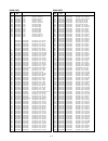
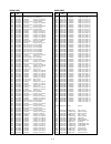
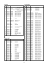
[main unit] [main unit] s.=surface mount d304 1790000620 s.Diode ma77 (tx) d305 1790000620 s.Diode ma77 (tx) d306 1790000620 s.Diode ma77 (tx) d401 1750000430 s.Diode hsb88wstr d501 1160000070 s.Diode dan202k t146 d502 1790001250 s.Diode ma2s111-(tx) d503 1160000070 s.Diode dan202k t146 d601 1160000...
Page 28
[main unit] [main unit] s.=surface mount l3502 6180000960 coil lal 03na 102k l4501 6200003950 s.Coil hf50acc 322513-t l4651 6200003950 s.Coil hf50acc 322513-t l4652 6200001830 s.Coil nl 322522t-100j l4653 6200003950 s.Coil hf50acc 322513-t l4654 6200003950 s.Coil hf50acc 322513-t l4656 6200001830 s....
Page 29
[main unit] [main unit] s.=surface mount r1523 7030003640 s.Resistor erj3geyj 473 v (47 k Ω ) r1601 7030003280 s.Resistor erj3geyj 470 v (47 Ω ) r1602 7030003400 s.Resistor erj3geyj 471 v (470 Ω ) r1603 7030003610 s.Resistor erj3geyj 273 v (27 k Ω ) r1604 7030003640 s.Resistor erj3geyj 473 v (47 k Ω...
Page 30
[main unit] [main unit] s.=surface mount r2901 7030003400 s.Resistor erj3geyj 471 v (470 Ω ) r2902 7030004040 s.Resistor erj3geyj 4r7 v (4.7 Ω ) r3001 7030003640 s.Resistor erj3geyj 473 v (47 k Ω ) r3002 7030003640 s.Resistor erj3geyj 473 v (47 k Ω ) r3003 7030003640 s.Resistor erj3geyj 473 v (47 k ...
Page 31
[main unit] [main unit] s.=surface mount c851 4030011600 s.Ceramic c1608 jb 1c 104kt-n c852 4030011340 s.Ceramic c1608 ch 1h 471j-t-a c853 4030007110 s.Ceramic c1608 ch 1h 680j-t-a c854 4030011280 s.Ceramic c1608 ch 1h 271j-t-a c855 4030010020 s.Ceramic c1608 jb 1h 122k-t-a c856 4030008770 s.Ceramic...
Page 32
[main unit] [main unit] s.=surface mount c2314 4030011600 s.Ceramic c1608 jb 1c 104kt-n c2315 4510005810 s.Electrolytic ecev1har47r c2352 4030006870 s.Ceramic c1608 jb 1h 222k-t-a c2353 4030011330 s.Ceramic c1608 ch 1h 391j-t-a c2354 4510004630 s.Electrolytic ecev1ca100sr c2380 4030011600 s.Ceramic ...
Page 33
[pll unit] [main unit] s.=surface mount j4801 6450001130 connector jpj2042-01-110 j5001 6450000140 connector hsj0807-01-010 j5101 6450001790 connector hlj7000-01-3010 w801 7030003860 s.Jumper erj3ge jpw v w1202 7030003860 s.Jumper erj3ge jpw v w1311 7030003860 s.Jumper erj3ge jpw v w1726 7030003860 ...
Page 34
[pll unit] [pll unit] s.=surface mount r105 7030003640 s.Resistor erj3geyj 473 v (47 k Ω ) r106 7030003640 s.Resistor erj3geyj 473 v (47 k Ω ) r107 7030003640 s.Resistor erj3geyj 473 v (47 k Ω ) r108 7030003640 s.Resistor erj3geyj 473 v (47 k Ω ) r116 7030003320 s.Resistor erj3geyj 101 v (100 Ω ) r1...
Page 35
[pa unit] [pll unit] s.=surface mount c224 4030011600 s.Ceramic c1608 jb 1c 104kt-n c225 4030006940 s.Ceramic c1608 ch 1h 030c-t-a c226 4030006940 s.Ceramic c1608 ch 1h 030c-t-a c227 4030007100 s.Ceramic c1608 ch 1h 560j-t-a j1 6510018960 s.Connector b2b-ph-sm3-tb j3 6510022000 s.Connector 16fmn-bmt...
Page 36
[filter unit] [pa unit] s.=surface mount c61 4030004740 s.Ceramic c2012 jb 1h 472k-t-a [eur], [ita], [fra], [esp] c62 4030005140 s.Ceramic c3216 jb 1e 104k-t-a [eur], [ita], [fra], [esp] c63 4510006650 s.Electrolytic ecev1ea100sr [eur], [ita], [fra], [esp] c68 4030011740 s.Ceramic grm42-2 ch 201j 50...
Page 37
[chassis parts] [filter unit] s.=surface mount c67 4010007590 ceramic hm15sj sl 681j 500v c68 4010005930 ceramic hm11sj sl 391j 500v c69 4010005930 ceramic hm11sj sl 391j 500v c70 4030006880 s.Ceramic c1608 jb 1h 472k-t-a c71 4030006880 s.Ceramic c1608 jb 1h 472k-t-a c72 4030006880 s.Ceramic c1608 j...
Page 38: Section 7
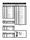
Mp1 8510013040 2241 mixer case 1 mp25 8510013140 dc-a case 1 f1 5210000080 fuse fgb 20a 1 f2 5210000130 fuse fgb 4a 1 mc1 optional product microphone hm-36 1 w1 optional product dc power cable opc-025 a 1 sp1 2510000670 speaker vs-50-0827 1 ep1 6910012480 sensor rms20-250-201-1r 1 ep2 6450001230 sna...
Page 39
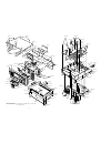
7 - 2 mp22 (c) mp26 (c) mp22 (c) mp22 (c) mp22 (c) mp22 (c) mp1 (l) mp3 (l) ds1 (l) ep70 (l) mp23 (f) mp23 (f) mp2 (c) mp2 (l) mp22 (f) mp22 (f) mp12 (c) mp24 (f) mp6 (f) mp2 (f) mp31(c) mp24 (f) mp6 (c) mp6 (c) mp1 (c) mp28 (c) mp22 (c) mp22 (c) mp28 (c) mp31 (c) mp8 (c) mp18 (c) mp22 (c) mp32 (c) ...
Page 40
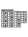
Section parts list section 8 semi-conductor informations 8-1 transistors name symbol inside view name symbol inside view 2sc1971 none 2sc3133 none b c e b c e 2sd1585k none b e c b e c 2sd1619-t-td db 2sd1664 t100q da b c c e 2sa1576a r fr c b e 2sc4673d-td co c e c b 2sk508 k52 2sk1740-ta ij g s d ...
Page 41
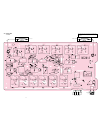
1 2 5 10 15 20 25 30 1 2 5 10 15 20 25 30 1 1 1 2 10 2 j201 j4001 j1 j701 to filter unit j1 from pll unit p4 gnd 1lo 1lo 1loe 1loe p1 p2 w6 to pa unit j6 w7 p5 p6 w10 to filter unit j3 w11 l3 l5 l2 l6 10 9 1 2 gnd t13v l3 ref l5 for l2 l4 l6 l1 t13v ref for l4 l1 2nd lo j401 j3601 1 2 from pll unit ...
Page 42
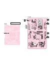
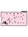
W2501 to main unit j9 15 16 1 2 gnd 8v 13v dnb dstb pdat con1 fskk nc 13v 13v pstb pck con2 con0 srst 2nd lo j1 1 2 1 2 to main unit j401 p2 p1 2lo 2loe bfo j2 j3 1 2 to main unit j2001 p5 bfo bfoe 1st lo j4 1 2 1 2 to main unit j201 p4 p3 1lo 1loe 9 - 2 main unit • bottm view 9-2 pll unit • top vie...
Page 43
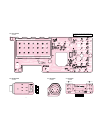
1 2 3 4 5 6 7 8 9 10 1 10 afgl afgl gnd gnd gnd rfgl rfgl gnd ritl ritl gnd sftl sftl gnd 5vl 5vl 5vl 5vl 5vl gnd to logic unit j3 shift rit rf/sql af j1 10 2 9 1 espo afo afo afe gnd espo espo afo afe afe to logic unit j5 j2 gnd gnd 6 8 5 4 3 2 1 7 9 - 3 9-3 logic board • top view 9-4 phone board •...
Page 44
6 8 5 4 3 2 1 7 gnd 8v send gnd mic gnd ud sqls afo mice to logic unit j4 j2 1 9 2 10 espo afo afo afe gnd espo espo afo afe afe to phone board j2 to vr board j1 j5 1 9 2 10 gnd gnd gnd gnd gnd afgl rfgl ritl sftl 5vl j3 1 2 10 9 sensor +5v sen1 sen2 gnd 1 4 mice afo sqls 8v gnd mic gnd send ud gnd ...
Page 45
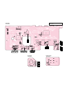
Antenna j1 1 3 5 7 9 2 4 6 8 10 to logic unit j4001 10 9 1 2 f1 f6 f4 f2 for f5 ref f3 t13v gnd j4 j3 p5 p6 to main unit j701 w11 w10 chassis j2 p4 p3 w9 to pa unit j7 w8 chassis 9 - 5 9-7 filter unit • top view the combination of this page and the next page shows the unit layout in the same configu...
Page 46
9 - 6 filter unit • bottom view the combination of this page and the previous page shows the unit layout in the same configuration as the actual p.C. Board..
Page 47
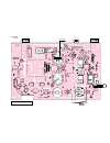
C14 c13 c16 c8 e b b e c b e c b e c e e c b e c e e b e e c e r30 d2 j3 to main unit j4101 1 1 5 10 15 15 16 16 2 2 gnd gnd pws gnd 14v 14v 14v 14v icl ich star temp 14v pat8 hv key j12 brown orange red yellow key star 14v gnd 1 2 3 4 1 2 3 4 5 6 j1 red red black black j6 p1 p2 w6 to main unit j1 w...
Page 48
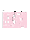
Varistor board 9 - 8 pa unit • bottom view the combination of this page and the previous page shows the unit layout in the same configuration as the actual p.C. Board..
Page 49
10 - 1 section 10 block diagram main unit q1508 2sc4081 q1509 dta114 afgv to mic ic2702 ta7368f d1901 1ss375 ic2001 ta4101 af select ic2101a njm2058 ic2801 tc4566 ic2901 la4425 ic2701 m5282fp side tone/beep ut-102 option ut-106 option vca ic2102 tc4w53 agc nbs d1501 1ss375 q1506 fi611 fl-65 q1603 3s...
Page 50
11 - 1 1 2 3 4 5 6 7 8 9 10 11 12 13 14 15 16 j3 gnd w4 1 2 3 4 5 6 7 8 9 10 11 12 13 14 15 16 j4101 1 2 3 4 5 6 7 8 9 10 11 12 13 14 15 16 17 18 19 20 21 22 23 24 25 26 27 28 29 30 j4401 chassis 1 2 3 4 5 6 7 8 9 10 11 12 13 14 15 16 17 18 19 20 21 22 23 24 25 26 27 28 29 30 j6 w2 front unit +5v se...
Page 51
Section 12 voltage diagram 12-1 filter, pa and main unit up ic-718 voltage diagram 153 210 12 - 1 up ic-718 voltage diagram 158 210 12 - 2 vr board rit shift r1 10k-b sql/rf af r2 10k-b r4 6.8k gnd gnd gnd gnd gnd sftl 5vl ritl rfgl afgl j1 j1 ud 8v mic mice gnd send afo sqls gnd gnd 10 9 8 7 6 5 4 ...
Page 52
Section 12 voltage diagram 12-1 filter, pa and main unit up ic-718 voltage diagram 153 210 12 - 1 up ic-718 voltage diagram 158 210 12 - 2 vr board rit shift r1 10k-b sql/rf af r2 10k-b r4 6.8k gnd gnd gnd gnd gnd sftl 5vl ritl rfgl afgl j1 j1 ud 8v mic mice gnd send afo sqls gnd gnd 10 9 8 7 6 5 4 ...
Page 53
Repair notes 1. Make sure a problem is internal before disassembling the transceiver. 2. Do not open the transceiver until the transceiver is disconnected from its power source. 3. Do not force any of the variable components. Turn them slowly and smoothly. 4. Do not short any circuits or electronic ...
Page 54
S-13701mz-c1 © 2000 icom inc. 6-9-16, kamihigashi, hirano-ku, osaka 547-0002, japan count on us! Hf tranceiver ic-718 ic-718.

