- DL manuals
- Icom
- Transceiver
- IC-91A
- Service Manual
Icom IC-91A Service Manual
Summary of IC-91A
Page 1
Service manual vhf/uhf fm transceiver s-14230hz-c1 may. 2006 vhf/uhf digital transceiver.
Page 2
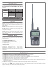
Introduction this service manual describes the latest service information for the ic-91a vhf/uhf fm transceiver , ic-91ad vhf/uhf digital transceiver at the time of publication. Ordering parts be sure to include the following four points when ordering replacement parts: 1. 10-digit icom parts number...
Page 3
Table of contents section 1 specifications section 2 inside views section 3 disassembly instructions section 4 ut-121 uninstallation section 5 circuit descripiton 5-1 receiver circuits. . . . . . . . . . . . . . . . . . . . . . . . . . . . . . . . . . . . . . . . . . . . . . . . . . . . . . . . 5-1 ...
Page 4: Section 1
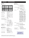
1 - 1 section 1 specifications general • frequency coverange : • operating mode : fm, am * , wfm * , dv † ( * rx only) • memory channels : 1304 channels (incl. 100 scan edges and 4 call ch.) • frequency stability : ±2.5 ppm (–20°c to +60°c; –4°f to 140°f) • tuning steps : 5 ‡ /6.25 ‡ /8.33 ‡ /9 ‡ /1...
Page 5: Section 2
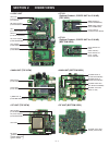
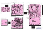
Section 2 inside views 2 - 1 • main unit (top view) • main unit (bottom view) • ut-121 (optional product ; codec unit for ic-91ad) (top view) • ut-121 (optional product ; codec unit for ic-91ad) (bottom view) • logic unit • rf unit (top view) • rf unit (bottom view) dc switch q1000: hat1026 d1000: m...
Page 6: Section 3
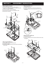
Section 3 disassembly instructions 3 - 1 • removing the rear panel 1 unscrew 2 screws a and remove the plate b . 2 remove the codec unit (ut-121) if installed. (see the page 4-1 “ 2 ” for uninstallation) 3 unscrew 2 screws c and 2 screws d . 4 disconnect the flat cable e from main unit j702. 5 remov...
Page 7: Section 4
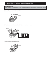
Section 4 ut-121 uninstallation 4 - 1 2 screws unit cover ut-121 (top view) notches tweezers q turn the power off, and remove the battery pack. W unscrew 2 screws to remove the unit cover. E insert the tweezers into the notches of the ut-121, and remove it as shown below. R screw 2 screws to assembl...
Page 8: Section 5
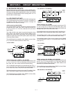
5-1 receiver circuits this transceiver has two receiving lines called a_band and b_ band for dualwatch capability. A_band corresponds to fm/wfm/ am mode receiving within 0.495–999 mhz range, and b_band corresponds to fm/fm-n/am/dv mode receiving within 118–174 mhz and 350–470 mhz ranges. 5-1-1 rf ci...
Page 9
5 - 2 • while receiving 350–470 mhz the 350–470 mhz band signals are passed through the lpf (l1– l3, c1–c6), hpf (l4, c7–c9) and attenuator (d7), then applied to the rf amplifier (q600) via the band switch (d600) and hpf (l600, l601, l608, l611, c600–c602, c630, c631, c633). The amplified signals ar...
Page 10
5 - 3 5-1-3 2nd if and demodulator circuits (main unit) the 1st if signal is converted into the 2nd if signal and demodulated in the if ic. The if ic contains 2nd mixer, limiter amplifier, quadrature detector, etc. In its package. 5-1-3-1 2nd if circuits - a_band (0.495–999 mhz) - • fm/am mode the 1...
Page 11
5 - 4 16 x200 w/n 11 10 b_band if ic (ic200) 9 13 12 “bnois” signal to the cpu (logic unit; ic1, pin 28) 1st if signal from the 1st if amplifier (q200) “brssi” signal to the cpu (logic unit; ic1, pin 46) 2 8 7 3 5 bpf (fm-n) (fm/am) rssi noise detector noise amplifier limitter amplifier quadrature d...
Page 12
5 - 5 the idc limits the level of the amplitude of mic signals to prevent over deviation. The limited mic signals are output from pin 7 and passed through the splatter filter (ic302, pins 8, 9). The splatter filter suppresses 3 khz and higher audio components. The filtered mic signals are applied to...
Page 13
5 - 6 5-2-4 apc circuit (rf unit) the apc (automatic power control) circuit stabilizes transmit output power and controls it high or low. The apc of this transceiver is a current monitoring type that detects the transmit signal current of the transmit amplifiers and controls the transmit output powe...
Page 14
5 - 7 5-3-2 pll circuits (rf and main units) the pll circuit provides stable oscillation of the transmit frequency and receive 1st lo frequency. The pll circuit compares the phase of the divided vco frequency with the reference frequency. The pll output frequency is controlled by the divided ratio (...
Page 15
5 - 8 input register osc counter pre- scaler phase detector charge pump loop filter x450 15.3 mhz 15.3/61.2 mhz 2nd lo signal 45.9 mhz 2nd lo signal 1 buffer amp. Q353 q450 9 10 11 “ck” 12 ×3 ×4 “bps” signal to the cpu (logic unit; ic1, pin 93) 15.3 mhz “ref” signal to the pll ic (rf unit; ic800, pi...
Page 16
5 - 9 pin no. Port name description 1 bled outputs tx/rx indicator (ds201) control signal to the tx/rx led driver (q201). “high”=while the squelch is open. 2 light outputs backlight control signal to the backlight leds driver (q203). “high”=while backlight is on. 3–7 kr0–kr4 input ports for keypad. ...
Page 17
5 - 10 pin no. Port name description 44 dtmf outputs dtmf/beep/1750 hz tone signals. 45 btone input port for tone signals (b_band; ctcss, dtcs, etc.) from the tone selector (main unit; ic703). 46 atone input port for tone signals (a_band; ctcss, dtcs, etc.) from the tone selector (main unit; ic703)....
Page 18: Section 6
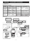
Section 6 adjustment procedures ¤ required test equipments equipment grade and range equipment grade and range dc power supply output voltage : 5.0–13.5 v dc current capacity : more than 2.5 a standard signal generator (ssg) frequency range : 0.1–1800 mhz output level : 0.1 µ v to 32 mv (–127 to –17...
Page 19
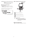
6 - 2 ¤ entering adjustment mode q turn the power off. W connect the jig cables (see page 6-1) to the [sp] and [mic] jacks. E while pushing [sql] and [8] keys, turn the power on. During adjustment mode, the function dispaly shows the adjustment item, frequency, etc. As below. ¤ quiting adjustment mo...
Page 20
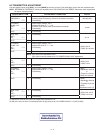
6-2 transmitter adjustment • set the specified value using [dial] , and push [band] to store the set value. Then push [2] to move to the next adjustment item. Note: “reference frequency” should be adjusted before “fm deviation” and “rxbpf.” otherwise, these adjustments will not be adjusted properly....
Page 21
6-2 transmitter adjustment (continued) • set the specified value using [dial] , and push [band] to store the set value. Then push [2] to move to the next adjustment item. Adjustment item adjustment condition value fm deviation [fmv] (/8 (vhf) 1 • connect an audio generator to the [mic] jack through ...
Page 22
6 - 5 6-3 receiver adjustment • set the specified value using [dial] , and push [band] to store the set value. Then push [2] to move to the next adjustment item. Adjustment item adjustment condition value rxbpf (a_band) [tra] 6t# • connect an ssg to the ant connector and set as; dev. : 3.5 khz af :1...
Page 23
6 - 6 6-4 receiver adjustment (continued) adjustment item adjustment condition value wfm s-meter [s3a] 5# • connect an ssg to the ant connector and set as; dev. : 3.5 khz af : 1 khz push [band] (automatic adjustment) 1.0–145 mhz bands 1 • set the ssg as; frequency : specified frequencies* level : 0 ...
Page 24
Adjustment item frequency (mhz) reference frequency [fr] 440.0 idling [id] 5.0 v vhf 145.0 (146.0)* uhf 435.0 (445.0)* final [po] 5.0 v vhf 145.0 (146.0)* uhf 435.0 (445.0)* idling [id] 7.4 v high vhf 145.0 (146.0)* uhf 435.0 (445.0)* low vhf 145.0 (146.0)* uhf 435.0 (445.0)* final [po] 7.4 v high v...
Page 25: Section 7
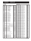
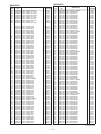
7 - 1 section 7 parts list m.=mounted side (t: mounted on the top side, b: mounted on the bottom side) [logic unit] ref order description m. H/v no. No. Location ic1 1140013020 s.Ic hd64f2238rtf13v b 29.9/78.2 ic2 1130013010 s.Ic sn74ahc1g08dck3 b 23.3/85.1 ic50 1130011770 s.Ic cd4066bpwr b 16.7/88....
Page 26
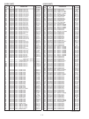
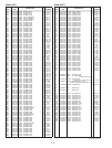
7 - 2 m.=mounted side (t: mounted on the top side, b: mounted on the bottom side) s.=surface mount [logic unit] ref order description m. H/v no. No. Location r323 7030007340 s.Res erj2gej 153 x (15 k ) b 35.9/52 r324 7030007340 s.Res erj2gej 153 x (15 k ) b 32.8/50 r325 7030007340 s.Res erj2gej 153 ...
Page 27
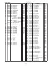
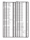
7 - 3 m.=mounted side (t: mounted on the top side, b: mounted on the bottom side) s.=surface mount [logic unit] ref order description m. H/v no. No. Location c346 4550007730 s.Tan teesvj 0j 106m8r b 18.7/46.7 c347 4030017460 s.Cer ecj0eb1e102k b 21.2/39.8 c348 4030018860 s.Cer ecj0eb0j105k b 17.6/46...
Page 28
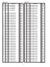
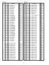
7 - 4 m.=mounted side (t: mounted on the top side, b: mounted on the bottom side) s.=surface mount [main unit] ref order description m. H/v no. No. Location l200 6200003540 s.Col mlf1608d r22k-t b 41.6/34.8 l201 6200003540 s.Col mlf1608d r22k-t b 42.2/33 l202 6200003540 s.Col mlf1608d r22k-t b 41.4/...
Page 29
7 - 5 m.=mounted side (t: mounted on the top side, b: mounted on the bottom side) s.=surface mount [main unit] ref order description m. H/v no. No. Location r650 7030005160 s.Res erj2gej 105 x (1 m ) t 20.3/9.7 r651 7030005050 s.Res erj2gej 103 x (10 k ) t 21.3/8.5 r652 7030005000 s.Res erj2gej 471 ...
Page 30
7 - 6 m.=mounted side (t: mounted on the top side, b: mounted on the bottom side) s.=surface mount [main unit] ref order description m. H/v no. No. Location c407 4030017420 s.Cer ecj0ec1h470j b 31.4/4.1 c408 4030017420 s.Cer ecj0ec1h470j b 29.7/6.6 c409 4030017420 s.Cer ecj0ec1h470j t 28.1/4.6 c410 ...
Page 31
7 - 7 m.=mounted side (t: mounted on the top side, b: mounted on the bottom side) s.=surface mount [rf unit] ref order description m. H/v no. No. Location ic100 1110005590 s.Ic µpc2762tb-e3 t 34/14.3 ic150 1110004050 s.Ic njm3404av-te1 t 43.8/34.7 ic800 1130013000 s.Ic lmx2313usldx/nopb t 20.6/21.9 ...
Page 32
7 - 8 m.=mounted side (t: mounted on the top side, b: mounted on the bottom side) s.=surface mount [rf unit] ref order description m. H/v no. No. Location l204 6200002041 s.Col nlv25t-101j b 11.6/33.1 l250 6200004590 s.Col mlf1608d r18k-t b 8.6/30.3 l251 6200004600 s.Col mlf1608d r15k-t b 8.2/29.1 l...
Page 33
7 - 9 m.=mounted side (t: mounted on the top side, b: mounted on the bottom side) s.=surface mount [rf unit] ref order description m. H/v no. No. Location r458 7030005090 s.Res erj2gej 104 x (100 k ) b 24.1/26.9 r459 7030005530 s.Res erj2gej 100 x (10) b 20.2/27.3 r460 7030005240 s.Res erj2gej 473 x...
Page 34
7 - 10 m.=mounted side (t: mounted on the top side, b: mounted on the bottom side) s.=surface mount [rf unit] ref order description m. H/v no. No. Location c114 4030017460 s.Cer ecj0eb1e102k t 48.1/24.7 c116 4030017640 s.Cer ecj0ec1h150j [usa], [usa-1] only t 48.5/25.9 c117 4030017460 s.Cer ecj0eb1e...
Page 35
7 - 11 m.=mounted side (t: mounted on the top side, b: mounted on the bottom side) s.=surface mount [rf unit] ref order description m. H/v no. No. Location c517 4030017640 s.Cer ecj0ec1h150j t 31.4/17.5 c518 4030017460 s.Cer ecj0eb1e102k t 30.9/37.9 c519 4030017630 s.Cer ecj0ec1h120j t 31.7/35.3 c60...
Page 36
7 - 12 m.=mounted side (t: mounted on the top side, b: mounted on the bottom side) s.=surface mount [vco unit] ref order description m. H/v no. No. Location q1 1530003560 s.Tr 2sc5195-t1 t 10.4/16.5 q2 1590003280 s.Tr unr9211j-(tx) t 4.6/15.1 q51 1530003560 s.Tr 2sc5195-t1 t 14/9.6 q52 1590003280 s....
Page 37
7 - 13 m.=mounted side (t: mounted on the top side, b: mounted on the bottom side) s.=surface mount [main unit] ref order description m. H/v no. No. Location ic1 1180002371 s.Reg r1111n321b-tr-f b 30.6/13.6 ic101 1130010920 s.Ic ambe-2020 t 25.4/10.7 ic102 1130011930 s.Ic sn74lvc1g04dckr b 29.9/17.3...
Page 38: Section 8
Section 8 mechanical parts and disassembly 8 - 1 screw abbreviations bt: self-tapping fh: flat head ph: pan head zk, ni-zk3: black ni-zu, ni-zc3: nickel-zinc sus: stainless ep4 ep2 mp1 mp3 mp2 ep1 *: refer to section 10 board layouts. [accessories] ep1 optional product antenna fa-s270c 1 ep2 optiona...
Page 39
Mp4 (l) unit abbreviations (c): chassis parts (l): logic unit (m): main unit (r): rf unit (v): vco unit mp1 (l) mp11 (l) mp2 (l) mp6 (l) mp3 (l) mp12 (l) sp1 (l) mp7 (l) mp10 (l) mp9 (l) mp9 (l) mp9 (l) mp9 (l) mp22 (l) mp9 (l) mp14 (l) s701 (m) j701 (m) j700 (m) mp300 (m) s702 (c) mp27 (c) mp9 (c) ...
Page 40: Section 9
Section 9 semiconductor information • transistors and fet's b e c b c e b b e e c c b e c b e c e c b e b e c b e c b e c b e c b e c g s d s d g g1 g2 s d d d d d g s s s e1 b1 b2 c1 c2 b e c b e c b e c g s d s b1 e b2 c1 c2 b1 e b2 c1 c2 e1 c2 b1 c1 e2 b2 e1 b2 e2 c1 c2 b1 e1 e2 b2 c1 b1 c2 2sa13...
Page 41: Section 10
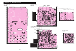
H5 h10 h15 h20 h25 h30 h35 h40 h45 h50 h0 v5 v10 v15 v0 v25 v30 v35 v20 v45 v50 v40 39 40 1 2 to logic unit j401 j702 extmic intsp clone diud dick vol s-lv intptt dafout chg ttemp unlk dastb1 iostb1 txc hv sql gnd data ck gnd afo aaf anois bnois brssi baf +3v atone btone iostb3 iostb2 bps bplstb ref...
Page 42
10 - 2 h5 h10 h15 h20 h25 h30 h35 h40 h45 h50 h0 v5 v10 v15 v0 v25 v30 v35 v20 v45 v50 v55 v40 v65 v70 v75 v60 v80 v90 v85 gnd 1 40 to main unit j702 j401 extmic afo intsp aaf clone anois diud bnois dick brssi vol baf s-lv +3v intptt atone dafout btone chg iostb3 ttemp iostb2 unlk bps dastb1 bplstb ...
Page 43: Section 11
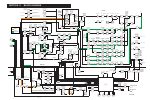
Section 11 block diagram 11 - 1 explanatory notes tx line rx line common line att agc det buff lpf j701 rf amp agc det bpf dc-dc tp76d96e20 s702 c a b hpf pll ic am det rf sw lpf hpf rf sw rf sw x3 bpf am det ant sw buff 1/2 ant sw amp rf sw rf sw rf amp rf amp amp 1 vco bc band 2 vco vhf band 3 vco...
Page 44: Section 12
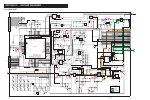
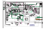
Section 12 voltage diagrams 12 - 1 voltage line explanatory notes tx line rx line common line j400 to codec unit j1 to main unit j702 to lcd sp1 + - 10k r114 4.7k r320 0 r66 1m r102 xp1501 q106 1 2 34 5 1k r301 1k r6 0.22 c65 1k r553 0.001 c107 unr9215j q306 sn74ahc1g08dck3 ic2 1 2 3 4 5 0.1 c16 1k ...
Page 45
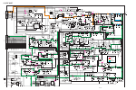
12 - 2 12-2 main unit voltage line explanatory notes tx line rx line common line j703 to rf unit j1001 lvifa ifa to logic unit j401 j702 47p c768 10p c767 10p c766 10p c765 47p c764 ck vcc data mod +5.5v sql plldata hv apllstb txc refmod iostb1 bplstb dastb1 bps unlk iostb2 ttemp iostb3 chg btone da...
Page 46
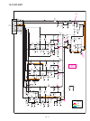
12 - 3 12-3 rf unit voltage line explanatory notes tx line rx line common line j1001 j800 to main unit j703 470p c908 47p c910 220p c907 47p c911 0.1u l900 220p c906 pllout to vco unit j1 rf unit 0.1 c256 8p c208 0.001 c162 hvc376b d402 0.001 c850 15p c103 0.001 c1006 220k r605 10n l704 2.2k r250 ma...
Page 47
12-4 vco unit voltage line explanatory notes tx line rx line common line j1 ulv loout uvco3 gnd gnd pllout mod gnd gnd bcvco3 vlv vshift vvco3 gnd gnd bclv to rf unit j800 0.001 c10 10k r4 47 r205 47 r53 1ss400 d53 0.001 c56 180 r200 0.01 c5 0.001 c114 47k r101 0.001 c1 0.001 c51 unr9211j q2 10k r55...
Page 48
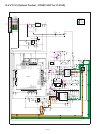
12-5 ut-121 (optional product ; codec unit for ic-91ad) voltage line explanatory notes tx line rx line common line 0.001 c214 100 r213 390k r211 0.1 c213 47p c110 22p c209 100k r305 120k r301 0.1 c104 0.1 c208 0.1 c303 47k r212 0.001 c111 22k r210 0.1 c113 100k r307 0.1 c109 0.027 c207 1 c304 22 c1 ...
Page 49
6f no.68, sec. 1 cheng-teh road, taipei, taiwan, r.O.C. Phone : +886 (02) 2559 1899 fax : +886 (02) 2559 1874 url : http://www.Asia-icom.Com e-mail : sales@asia-icom.Com zac de la plaine, 1, rue brindejonc des moulinais bp 5804, 31505 toulouse cedex, france phone : +33 (5) 61 36 03 03 fax : +33 (5) ...
Page 50
1-1-32, kamiminami, hirano-ku, osaka 547-0003, japan s-14230hz-c1 © 2006 icom inc..

