- DL manuals
- Icom
- Transceiver
- IC-E90
- Service Manual
Icom IC-E90 Service Manual
Summary of IC-E90
Page 1
S-13903mz-c2 2002 icom inc. 1-1-32, kamiminami, hirano-ku, osaka 547-0003, japan multiband fm transceiver i e90 ic-e90 ic-e90 (1,4).
Page 2
Introduction this service manual describes the latest service information for the ic-e90 multiband fm transceiver at the time of publication. E90 model version symbol europe europe-1 united kingdom italy spain france eur eur-1 uk itr esp fra to upgrade quality, all electrical or mechanical parts and...
Page 3
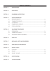
Table of contents section 1 specifications section 2 inside views section 3 disassembly instructions section 4 circuit description 4 - 1 receiver circuits ................................................................................................... 4 - 1 4 - 2 transmitter circuits ...............
Page 4
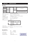
1 - 1 m general • frequency range : (unit: mhz) • mode : fm, am (rx only) and wfm (rx only) • number of memory channels : 555 (incl. 50 scan edges and 5 call channels) • frequency stability : ±6 ppm max. ( –10˚c to +60˚c; 14˚f to 140˚f) • tuning steps : 5, 6.25, 8.33, 9, 10, 12.5, 15, 20, 25, 30, 50...
Page 5
1 - 2 all stated specifications are subject to change without notice or obligation. M receiver • receiver system : double-conversion superheterodyne • intermediate frequency : 1st 13.350 mhz (fm/am) 13.350 mhz (wfm) 2nd 450 khz • sensitivity* 1 : (except spurious points; typical values) * 1 fm and w...
Page 6
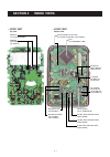
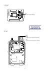
2 - 1 section 2 inside views eeprom (ic2: hn58x24128fpi, q2: un9115) reset ic (ic142: s-80928cnmc) crystal oscillator for cpu clock (x1: cr-687, 6.7584 mhz, q40: un9215) cpu (ic1: m30220ma-114rp) af regulator (q201: 2sb1201, q202: xp1501) +3 regulator (q8: 2sb1132, q9: xp1501) +3c regulator (q142: x...
Page 7
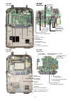
2 - 2 50 mhz tx low-pass filter circuit 144 mhz tx high-pass filter circuit pre-drive (q54: 2sc5289) drive amplifier (q52: 2sk3475) 0.495–29.995 mhz rf amplifier (q302: 2sc5006) 75.995–229.995 mhz rf amplifier (q351: 3sk320) r3 regulator (q353: xp4312) 29.995–75.995 mhz rf amplifier (q303: 2sc5006) ...
Page 8
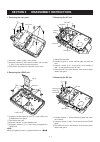
3 - 1 section 3 disassembly instructions 1. Removing the rear panel 2. Removing the logic unit 3. Removing the af unit 4. Removing the rf unit q unscrew 1 screw a (m2 × 4 mm, black) . W unscrew 2 screws b (m2 × 20 mm, black), and 4 screws c (m2 × 6 mm, black) from the rear panel. E take off the rear...
Page 9
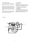
Section 4 circuit description 4 - 1 4-1 receiver circuits 4-1-1 triplexer circuit (rf unit) the transceiver has a triplexer (low-pass and bandpass fil- ters) on the first stage from the antenna switching diode to separate the signals. • rf signals 0.495 mhz–75.995 mhz the 0.495 mhz–75.995 mhz rf sig...
Page 10
4 - 2 (3) 76.0 mhz–229.995 mhz rf circuit the signals from the antenna switching circuit pass through the attenuator (d351), and then applied to the bandpass fil- ter (d352, d353, l351, l352) to suppress unwanted signals. The signals pass through the bandpass filter (d354–d356, d359, l354, l355, l35...
Page 11
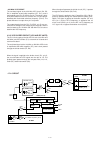
4 - 3 (1) am detector circuit the filtered signals are applied to the am detector circuit (q201, q202) to demodulate the 2nd if signal into the am af signals. (2) fm and wfm detector circuit the filtered signals are applied to the limiter amplifier section in the fm if ic (ic151, pin 5), and then ap...
Page 12
4 - 4 4-1-8 agc circuit (af and rf units) the agc (automatic gain control) circuit reduce signal fad- ing and keeps the audio output level constant. A portion of af signals from the am detector circuit (q201) are applied to the amplifier (q202). The amplified dc voltage from the q202, pin 4 is appli...
Page 13
4 - 5 4-2-5 apc circuit (rf unit) the apc circuit protects the power amplifier from a mis- matched output load and stabilizes the output power. The apc circuit is designed to use vhf and uhf bands com- monly. The apc sensor (r109) detects driving current from the drive voltage at the drive (q52) and...
Page 14
4 - 6 • 430 mhz vco circuit the oscillated signal at the 430 mhz vco circuit (q4, q5, d3) is amplified at two buffer amplifiers (q7, q11), and is then applied to the pll ic (ic201, pin 19). The signal is divid- ed by serial data from the cpu (logic unit; ic1) and phase- detected with the divided ref...
Page 15
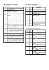
4 - 7 line hv vcc cpu3 +3c +3 +10v afv r3 r3v t3 description the voltage from the external power supply or attached battery pack. The same voltage as the “hv” line (external power supply or battery pack). Common 3 v converted from the “vcc” line by cpu3 regulator ic (logic unit; ic141). The out- put...
Page 16
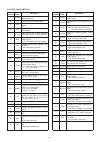
4 - 8 pin port description number name pin port description number name 1 3 5 6 7 12 13 14 19 25 26 28 29 30 31 33 34 35 40 42 43 44 45 patmp sd chg vin ctcin wfm am clsft reset power cpuhv iostb dastb clin clout pdaul ck plstb eck chgc pcon r3c txc input port for the pa’s temperature while transmit...
Page 17
4 - 9 pin port description number name 84 85 86 88–90 92 94–96 97 98 99–127 128–131 138 139 141 144 50m ctsel dtcs seg37– seg35 seg34 seg33– seg31 cont1 cont0 seg28– seg0 com3– com0 volc ctcout beep wxalt outputs the 50 mhz modulation circuit control signal. Low: while 50 mhz is transmitting. Output...
Page 18
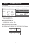
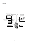
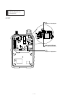
5 - 1 5-1 preparation some adjustments must be adjusted on the adjustment mode. When entering the adjustment mode, the 68 k Ω terminator (as shown at page 5-2) is required. ‘ ‘ required test equipment ‘ ‘ entering the adjustment mode q connect a 68 k Ω terminator to the [sp] jack. W push and hold th...
Page 19
5 - 2 to [mic] to the antenna connector rf power meter 0.1 10 w/50 frequency counter attenuator 40 db or 50 db fm deviation meter standard signal generator 0.1 v to 32 mv ( 127 dbm to 17 dbm) audio generator caution: do not transmit while an ssg is connected to the antenna connector. Optional sma bn...
Page 20
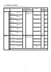
5 - 3 5-2 trimmer adjustment the following adjustment must be performed on the normal mode. Pll lock voltage power balance adjustment adjustment adjustment condition measurement value point unit location unit adjust 1 2 3 4 5 6 1 2 3 4 5 • displayed frequency : 30.000 mhz • mode : fm • receiving • d...
Page 21
5 - 4 cp pll lock voltage check point l456 l16 tx power balance adjustment (435 mhz) l19 tx power balance adjustment (145 mhz) • vco unit • rf unit.
Page 22
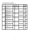
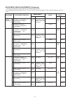
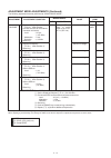
5 - 5 5-3 adjustment mode adjustments the following adjustment must be performed at “adjustment mode”. Reference frequency output power (11v 50 mhz high power) (11v 145 mhz high power) (11v 440 mhz high power) (11v 50 mhz low power) (11v 145 mhz low power) adjustment adjustment adjustment condition ...
Page 23
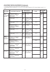
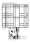
5 - 6 adjustment mode adjustments (continued) • the following adjustment must be performed at “adjustment mode”. • the adjustment channel indicators (pl, dl, ph, dh, pe, de) need to change from “dh” channel indicator to push “0” or “.” keys. Output power (11 v 440 mhz low power) output power (8v 50 ...
Page 24
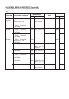
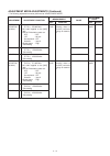
5 - 7 adjustment mode adjustments (continued) • the following adjustment must be performed at “adjustment mode”. • the adjustment channel indicators (pl, dl, ph, dh, pe, de) need to change from “dh” channel indicator to push “0” or “.” keys. Output power (8v 50 mhz low power) (8v 145 mhz low power) ...
Page 25
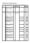
5 - 8 adjustment mode adjustments (continued) • the following adjustment must be performed at “adjustment mode”. • the adjustment channel indicators (pl, dl, ph, dh, pe, de) need to change from “dh” channel indicator to use “0” or “.” keys. Output power (5v 50 mhz) (5v 145 mhz) (5v 440 mhz) adjustme...
Page 26
5 - 9 adjustment mode adjustments (continued) • the following adjustment must be performed at “adjustment mode”. Fm deviation (50 mhz) (145 mhz) (440 mhz) dtmf deviation (50 mhz) (145 mhz) (440 mhz) adjustment adjustment adjustment condition measurement value point unit location unit adjust 1 2 3 1 ...
Page 27
5 - 10 adjustment mode adjustments (continued) • the following adjustment must be performed at “adjustment mode”. Ctcss deviation (50 mhz) (145 mhz) (440 mhz) dtcs deviation (50 mhz) (145 mhz) (440 mhz) adjustment adjustment adjustment condition measurement value point unit location unit adjust 1 2 ...
Page 28
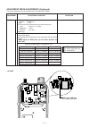
5 - 11 adjustment mode adjustments (continued) the following adjustment must be performed at “adjustment mode”. “detector coil” adjustment must be performed on same channel as “dtcs deviation adjustment” (dt ch.). Detector coil rf tracking adjustment adjustment adjustment condition measurement value...
Page 29
Ic151, pin 12 (sd line) rf tracking check point l151 detector coil adjustment cp0 detector coil check point note: a : [eur], [itr], [uk] only b : except [esp] 5 - 12 • af unit.
Page 30
5 - 13 rf tracking adjustment mode adjustments (continued) the following adjustment must be performed at “adjustment mode”. Adjustment adjustment adjustment condition measurement value point unit location unit adjust 11 12 13 14 15 16 • displayed frequency : (tm ch.) 430.100 mhz • connect the ssg to...
Page 31
5 - 14 adjustment mode adjustments (continued) the following adjustment must be performed at “adjustment mode”. S-meter adjustment adjustment condition operation 1 2 • displayed frequency : (sm ch.) 1.620 mhz b • mode : fm • connect the ssg to the antenna connector and set as: level : 0.63 µv * (–11...
Page 32
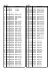
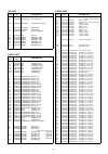
S.=surface mount ic51 1110005590 s.Ic µpc2762tb-e3 ic101 1110004050 s.Ic njm3404av-te1 ic251 1110004530 s.Ic m62368gp 70ed ic351 1110005230 s.Ic µpc2757tb-e3 q1 1590001150 s.Transistor un9211 (tx) q2 1590001860 s.Transistor un9215 (tx) q51 1560001150 s.Fet 2sk3476 (te12l) q52 1560001160 s.Fet 2sk347...
Page 33
6 - 2 s.=surface mount l452 6200005610 s.Coil eljre 3n9z-f l453 6200005610 s.Coil eljre 3n9z-f l454 6200006980 s.Coil eljre r10g-f l455 6200005720 s.Coil eljre 33ng-f l456 6200010240 s.Coil 0.4-0.8-2tl r1 7030009280 s.Resistor erj2ge r2 7030004980 s.Resistor erj2gej 101 x (100 Ω ) r6 7030004980 s.Re...
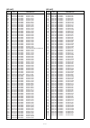
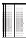
Page 34
S.=surface mount c60 4030017510 s.Ceramic ecj0ec1h680j c62 4030016790 s.Ceramic ecj0eb1c103k c64 4030017330 s.Ceramic ecj0ef1c104z c65 4030017640 s.Ceramic ecj0ec1h150j c66 4030017460 s.Ceramic ecj0eb1e102k c67 4030016790 s.Ceramic ecj0eb1c103k c68 4030017660 s.Ceramic ecj0ec1h330j c69 4030017460 s....
Page 35
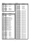
6 - 4 s.=surface mount j251 6510022860 s.Connector axk6s30445p j252 6450000870 connector hec2711-01-020 w1 7030010040 s.Jumper erj2ge-jpw w2 7030010040 s.Jumper erj2ge-jpw ep1 0910055443 pcb b 5845c ep2 6910013310 s.Bead mmz1608d121b ep3 6910014640 s.Bead mpz2012s221a-t ep4 6910014640 s.Bead mpz2012...
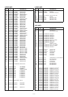
Page 36
S.=surface mount r216 7030008290 s.Resistor erj2gej 183 x (18 k Ω ) r217 7030008290 s.Resistor erj2gej 183 x (18 k Ω ) r218 7030005050 s.Resistor erj2gej 103 x (10 k Ω ) r219 7030008290 s.Resistor erj2gej 183 x (18 k Ω ) r220 7030005090 s.Resistor erj2gej 104 x (100 k Ω ) r221 7030005050 s.Resistor ...
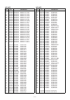
Page 37
6 - 6 s.=surface mount j252 6450001680 connector hsj1122-010010 j253 6450002250 connector hsj1456-010320 s251 7600000210 encoder tp70n00e20-15f-1903 w1 7030010040 s.Jumper erj2ge-jpw w2 7030010040 s.Jumper erj2ge-jpw w3 9014505003 wire 22/07/070/w02/w02 ep1 0910054435 pcb b 5735e ep3 6910012350 s.Be...
Page 38
S.=surface mount r85 7030005050 s.Resistor erj2gej 103 x (10 k Ω ) r88 7030005050 s.Resistor erj2gej 103 x (10 k Ω ) r89 7030005240 s.Resistor erj2gej 473 x (47 k Ω ) r91 7030005050 s.Resistor erj2gej 103 x (10 k Ω ) r92 7030004970 s.Resistor erj2gej 470 x (47 Ω ) r93 7030004970 s.Resistor erj2gej 4...
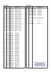
Page 39
6 - 8 s.=surface mount c198 4030017460 s.Ceramic ecj0eb1e102k c199 4030017460 s.Ceramic ecj0eb1e102k c200 4030017460 s.Ceramic ecj0eb1e102k c205 4550006210 s.Tantalum ecst1cx106r c207 4030011810 s.Ceramic c1608 jb 1a 224k-t c208 4030017460 s.Ceramic ecj0eb1e102k c209 4030017460 s.Ceramic ecj0eb1e102...
Page 40
S.=surface mount r45 7030005040 s.Resistor erj2gej 472 x (4.7 k Ω ) r46 7030007570 s.Resistor erj2gej 122x (1.2 k Ω ) r47 7030005040 s.Resistor erj2gej 472 x (4.7 k Ω ) r48 7030004990 s.Resistor erj2gej 221 x (220 Ω ) r49 7030008410 s.Resistor erj2gej 392 x (3.9 k Ω ) r50 7030005040 s.Resistor erj2g...
Page 41
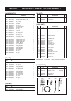
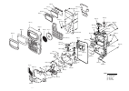
7 - 1 ep2 ep3 mp1 mp2 ep1 section 7 mechanical parts and disassembly j1 6510022671 connector sma-r235-1 1 mp1 8210018240 panel 2507 rear panel 63-222 1 mp2 8930054200 2372 jack cap 1 mp3 8930056321 2507 dc cap-1 1 mp4 8310050390 2372 lock plate 1 mp5 8610010990 knob n284 1 mp6 8930054290 2372 main s...
Page 42
7 - 2 mp11 (r) mp10 (r) mp8 (r) mp18 (r) mp29 (c) mp30 (c) mp31 (c) mp9 (c) s251(a) mp21 (c) mp3 (c) mp15 (c) mp6 (c) mp8 (l) mp12 (l) mp11 (c) mp22 (c) mp12 (c) mp24 (c) mp24 (c) mp5 (c) mp2 (c) mp1 (c) mp12 (c) mp25 (c) mp8 (c) mp26 (c) mp4 (c) mp10 (c) mp9 (r) mp2 (r) mp6 (r) mp1 (r) mp1 (v) mp2 ...
Page 43
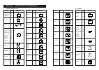
8 - 1 section parts list section 8 semi-conductor information 8 - 1 transistors and fets 8 - 2 diodes name symbol inside view 1ss364 bf ma132wk mu c a1 a2 1ss362 c3 1ss372 n9 ma133 mp a c ma6s121 m2d a1 c1 a2 c2 a3 c3 1sv307 tx a c ma132hk m3n a c 1sv271 tg 1sv290 tj 1sv308 tx hvc132 p2 hvc136 trf p...
Page 44
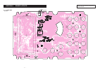
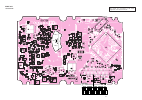
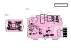
Mc1 microphone pwr band d 1 v ↔ d 2 tone 3 h/l mode scan vfo mhz 4 dup 5 skip 6 m.N 0 rit mr s.Mw 7 tscan 8 set 9 ts . Dtmf.M call tv lock the combination of this page and the next page shows the unit layout in the same configuration as the actual p.C. Board. 9 - 1 9 - 1 logic unit • top view sectio...
Page 45
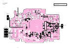
1 1 2 39 40 2 39 40 gnd intsp ck pdaul am iostb data dick remo v3c v1c noise beep hv volc +3c afv vmod chg gnd +10v wxalt plstb wfm txc dastb diud r3c sd v2c vsft extm mute vcc deto +3 xmod patmp gnd gnd sql ptt to af unit j251 sp1 w2 (l) w2 (l) the combination of this page and the previous page sho...
Page 46
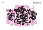
6 1 6 1 8 1 to vco unit j2 lo v3 +3 v2 v1 gnd 8 1 to vco unit j1 1 15 30 16 1 15 30 16 to af unit j51 j251 antenna ref plstb ck pda/ul +10v gnd vmod vshft ck data plstb dastb t43 t50 t14 b4c agc b1c vcc b5c b3c gnd ref pda/ul vmod hv vshft +3 patmp b2c +10v bsft v2 fset v3 v1 if chg the combination ...
Page 47
The combination of this page and the previous page shows the unit layout in the same configuration as the actual p.C. Board. Rf unit • bottom view 9 - 4.
Page 48
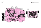
9 - 5 9 - 3 af unit • top view vco unit • top view 1 2 39 40 3 3 1 2 4 2 1 dn e up to s251 40 39 2 1 gnd chg vmod afv +3c volc hv beep noise v1c v3c remo dick data iostb am pda/ul ck intsp gnd to logic unit j1 ext.Mic j252 ext.Sp remoto j253 j251 gnd gnd patmp xmod +3 deto vcc mute extm vshft v2c sd...
Page 49
9 - 6 vco unit • bottom view 1 2 3 2 1 3 4 s251 s253 s252 up e dn 1 15 30 16 to rf unit j251 j51 ck data plstb dastb t43 t50 t14 b4c agc b1c vcc b5 b3 gnd ref pda/ul vmod hv vshft +3 patmp b2c +10v bsft v2 fset v3 v1 if chg the combination of this page and the previous page shows the unit layout in ...
Page 50
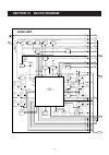
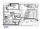
10 -1 section 10 block diagram cpu lcd lpf +3 reg lpf lpf eeprom key init matrix hv sens tx sens mic mute mic amp dev change mod sw ct/dt sw led ctrl led ctrl led ctrl led led led led3 reg +3c reg cpu3 reg chg reset pcon chgc cpu3 chg chg chg hv patmp vcc ct3 sw mic3 sw clone buff intsp vmod xmod mu...
Page 51
10 - 2 af unit chassis rf unit vco unit patmp wxalt ant lpf lpf lpf hpf hpf hpf ant sw ant sw ant sw lpf bpf hpf amp lpf drive amp drive pre buff tx/rx sw bpf bpf bpf bpf bpf rf amp rf amp rf amp rf amp rf amp bpf bpf rf amp rf amp bpf bpf bpf bpf if amp bpf am det lpf af amp af mute af amp hpf lo a...
Page 52
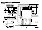
11 - 1 11 - 1 logic unit section 11 voltage diagram afon cpuhv ptt +3cpu +3 vin mute micc pcon chgc esio eck ctsel led3 ctcin +10v ctcout la lb lc c88 68p c5 0.001 r27 47k c90 0.001 c20 22p r53 68k r17 1k r91 10k c401 1 r146 10k s1008 s1018 d141 ma2s111 s1021 c95 1 r14 47k r28 1k c96 1 s1007 r10 10k...
Page 53
11 - 2 afon cpuhv ptt ptt +3cpu +3 vin mute micc pcon chgc afon mute chgc esio eck ctsel led3 ctcin +10v ctcout la lb lc c316 4.7 c45 0.001 r243 82k c162 0.001 r151 1k r88 10k r454 1k r302 330 1 2 3 5 c198 0.001 c451 0.01 c41 0.001 c143 0.001 c243 0.1 r312 120 c200 0.001 r301 5.6k c146 0.1 c205 10 1...
Page 54
11 - 3 c220 0.001 c205 0.001 c204 0.001 c472 470p c489 0.01 c416 10p r59 1.5k r460 220 l51 24nh c69 0.001 r353 68k c106 0.001 fi1 glp10-512m i o r456 220 r352 4.7k c365 0.001 c33 10p c461 0.001 r41 4.7k r363 1.2k l304 0.22 µ h l252 exccl3225u r106 10k l451 3.3nh 5 d 6 d 7 d 8 d 1 s 2 s 3 s 4 g c303 ...
Page 55
11 - 4 o r101 4.7k c101 0.01 c103 4p c109 100p l101 0.82 µ h l103 1.5 µ h c105 0.01 c110 0.001 r105 4.7k c113 0.01 r108 6.8k r107 15k r109 47 c115 0.001 c114 8p r111 220 l104 1.0 µ h d103 ma133 c153 0.01 c116 0.01 r158 220k c161 0.001 c160 0.001 r159 4.7k c158 0.001 r156 15k r155 56k r167 220k c156 ...
Page 56
Introduction this service manual describes the latest service information for the ic-e90 multiband fm transceiver at the time of publication. E90 model version symbol europe europe-1 united kingdom italy spain france eur eur-1 uk itr esp fra to upgrade quality, all electrical or mechanical parts and...
Page 57
S-13903mz-c2 2002 icom inc. 1-1-32, kamiminami, hirano-ku, osaka 547-0003, japan multiband fm transceiver i e90 ic-e90 ic-e90 (1,4).

