- DL manuals
- Icom
- Transceiver
- IC-F3021S
- Service Manual
Icom IC-F3021S Service Manual
Summary of IC-F3021S
Page 1
Service manual vhf fm transceivers s-14303hz-c1 july 2006.
Page 2
This service manual describes the latest service information for the ic-f3021t/s, ic-f3022t/s and ic-f3023t/s vhf fm transceivers at the time of publication. Be sure to include the following four points when ordering replacement parts: 1. 10-digit icom parts numbers 2. Component name and information...
Page 3
Table of contents section 1 specifications section 2 inside views section 3 disassembly instructions section 4 optional unit installation section 5 circuit descripiton 5-1 receiver circuits. . . . . . . . . . . . . . . . . . . . . . . . . . . . . . . . . . . . . . . . . . . . . . . . . . . . . . . ....
Page 4: Section 1
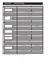
1 - 1 section 1 specifications [usa], [gen] [eur] general • frequency coverage 136–174 mhz • type of emission wide 16k0f3e (25.0 khz) middle – 14k0f3e (20.0 khz) narrow 11k0f3e (12.5 khz) 8k50f3e (12.5 khz) • number of programable channels 128 channels (8 zones) • antenna impedance 50 Ω (nominal) • ...
Page 5: Section 2
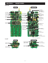
Section 2 inside views 2 - 1 apc amplifier (ic701: ta75s01f) power amplifier (q701: rd07mvs1) drive amplifier (q702: rd01mus1) antenna switch (d701: 1sv307) lcd driver (ic20: lc75834w) +5 regulator q26: 2sb1132 q27: xp6501 q28: unr9213j cpu (ic22: hd64f2238btf13v) eeprom (ic10: hn58x2464ti) reset ic...
Page 6: Section 3
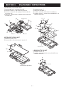
Section 3 disassembly instructions 3 - 1 2 removing the main unit q remove the main seal f. W unscrew vr nut g, and remove the top plate h. 3 removing the pa unit q unscrew 3 screws m. W unsolder 4 points n, and take off the pa unit in the direction of the arrow. 1 removing the chassis unit q unscre...
Page 7: Section 4
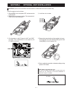
4 - 1 section 4 optional unit installation caution! Optional unit installation should be done at authorized icom servise center only. Install the optional unit as follows. Q rotate [vol] to turn the power off, and remove the battery pack. W remove the unit cover as below. (the removed unit cover can...
Page 8: Section 5
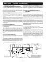
Section 5 circuit description 5 - 1 5-1 receiver circuits 5-1-1 antenna switching circuit (pa unit) the antenna switching circuit toggles the receive (rx) line and transmit (tx) line. The received signals from the antenna are passed through the low-pass filter (ant unit; l801, l802, c802, c803, c807...
Page 9
5 - 2 the af signals from the analog switch (ic3, pin 11) are applied to the volume buffer amplifi er (ic6, pin 9). The buffer- amplified af signals are adjusted its level (= audio level) by volume control pot (r315), then applied to the af power amplifier (ic15, pin 4) and amplified to the 0.5 w of...
Page 10
5 - 3 5-2-3 transmit amplifiers (pa unit) the transmit signal from the vco is amplifi ed to the transmit output level by the transmit amplifi ers. The transmit signal from the tx/rx switches (main unit; d16 is on, d17 is off) is amplifi ed by the pre-drive amplifi er (q704), drive amplifi er (q702) ...
Page 11
5 - 4 5-3 pll circuits 5-3-1 voltage controlled oscillators (vcos; main unit) vco is an oscillator whose oscillating frequency is controlled by adding voltage (lock voltage). This transceiver has 2 vcos rx vco (q17, d9, d11, d33) and tx vco (q16, d10, d13, d34). The rx vco oscillates the 1st lo sign...
Page 12
5 - 5 cpu5v regurator +5v regurator s5v regurator t5v regurator r5v regurator power switch r315 f701 (pa unit ) q26–q28 ic17 q23 q24, q49 q25 vcc cpu5 cpu +5v s5v “s5c” “pwon” voltage line control signal 8 22 87 88 “t5c” “r5c” t5v led backlight driver (q45), lcd driver (ic20), d/a converter (ic12), ...
Page 13
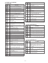
5 - 6 5-5-1 cpu (ic22) pin no. Port name description 1−3 kr1− kr3 input ports for dealer-programmable keys. 4−8 ks0− ks4 output ports for dealer-programmable keys. 9 busy outputs “busy” signal to the dsp unit. 10 ccs outputs chip-select signal to the dsp unit. 11 sck outputs serial clock signal to t...
Page 14: Section 6
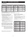
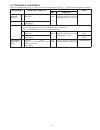
Section 6 adjustment procedures 6-1 preparation when adjusting ic-f3020 series, cs-f3020 cloning software, cs-f3020 adj adjustment software (rev. 1.0 or later), opc-478/u jig cable (modifi ed opc-478/u cloning cable ; see the page 6-2) and the following test equipments are required. Equipment grade ...
Page 15
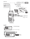
6 - 2 ic-f3020 series fm deviation meter osciiloscope to the antenna connector attenuator 10 db or 20 db rf power meter 0.1–10 w/50 frequency counter standard signal generator 0.1 µv to 32 mv (–127 dbm to –17 dbm) caution! Do not transmit while the ssg is connected to the antenna connector sinad met...
Page 16
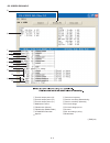
6 - 3 • pc screen exsample reference frequency receive sensitivity (manually) pll lock voltage preset s-meter reload data pll lock voltage (verify) squelch *; [eur] only ctcss/dtcs deviation fm deviation (narrow) fm deviation (middle*/wide) modulation balance transmit output power (hi) transmit outp...
Page 17
6 - 4 6-2 frequency adjustment select an adjustment item using [ ↑] / [↓] keys, then set to the specifi ed value using [←] / [→] keys on the connected pc’s keyboard. Adjustment adjustment condition measurement value unit operation pll lock voltage [rx lva] 1 • channel • receiving : ch 1 pc screen cl...
Page 18
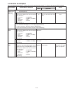
6 - 5 6-3 transmit adjustment select an adjustment item using [ ↑] / [↓] keys, then set to the specifi ed value using [←] / [→] keys on the connected pc’s keyboard. Adjustment adjustment condition measurement value unit operation output power [power (hi)] 1 • channel • transmitting : ch 3 top panel ...
Page 19
6 - 6 6-4 receive adjustment select an adjustment item using [ ↑] / [↓] keys, then set to the specifi ed value using [←] / [→] keys on the connected pc’s keyboard. Adjustment adjustment condition measurement value unit location receive sensitivity [bpf (t1)] [bpf (t2)] note: “receive sensitivity” mu...
Page 20: Section 7
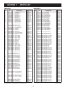
7 - 1 section 7 parts list m.=mounted side (t: mounted on the top side, b: mounted on the bottom side) [main unit] ref order description m. H/v no. No. Location ic2 1140005991 s.Ic mb15a02pfv1-g-bnd-ere1 t 81.2/34.5 ic3 1130011770 s.Ic cd4066bpwr b 40.4/22 ic5 1110005320 s.Ic njm13403v-te1 b 40.4/12...
Page 21
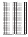
7 - 2 m.=mounted side (t: mounted on the top side, b: mounted on the bottom side) s.=surface mount [main unit] ref order description m. H/v no. No. Location r99 7030007340 s.Res erj2gej 153 x (15 k ) b 79.6/34.7 r100 7030005040 s.Res erj2gej 472 x (4.7 k ) t 74.4/21.6 r101 7030004990 s.Res erj2gej 2...
Page 22
7 - 3 m.=mounted side (t: mounted on the top side, b: mounted on the bottom side) [main unit] ref order description m. H/v no. No. Location c27 4030017430 s.Cer ecj0ec1h101j b 100.4/40.4 c28 4030017360 s.Cer ecj0ec1h030b b 97.4/39.5 c29 4030017580 s.Cer ecj0ec1h060c b 95.8/36.5 c30 4030017460 s.Cer ...
Page 23
7 - 4 m.=mounted side (t: mounted on the top side, b: mounted on the bottom side) s.=surface mount [main unit] ref order description m. H/v no. No. Location c315 4030016930 s.Cer ecj0eb1a104k b 43.2/37 c316 4030017420 s.Cer ecj0ec1h470j b 53.3/32 c317 4030016790 s.Cer ecj0eb1c103k b 55/33 c318 40300...
Page 24
7 - 5 m.=mounted side (t: mounted on the top side, b: mounted on the bottom side) s.=surface mount [pa unit] ref order description m. H/v no. No. Location c701 4030017460 s.Cer ecj0eb1e102k t 35/11 c702 4030017430 s.Cer ecj0ec1h101j b 33.8/10 c703 4030017420 s.Cer ecj0ec1h470j b 34.8/10 c704 4030017...
Page 25
7 - 6 m.=mounted side (t: mounted on the top side, b: mounted on the bottom side) s.=surface mount [main unit] ref order description m. H/v no. No. Location ic1 1110006480 s.Ic njm2801u1-0543-te1 b 10.2/62.3 ic2 1110003071 s.Ic µpc494gs-e1-a b 13/36.7 ic3 1140012301 s.Ic µpd789112amc-534-5a4-a b 19....
Page 26: Section 8
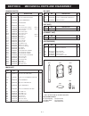
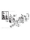
Section 8 mechanical parts and disassembly 8 - 1 screw abbreviations bt: self-tapping ph: pan head zk, zk3: black fh: flat head ni: nickel sus: stainless ep1 ep2 mp1 mp2 mp3 mp4 j1 6910015910 connector ant connector-104 1 j2 6910015860 connector imsa-6277s-02a-g 1 sp1 2510001060 speaker k036na500-47...
Page 27
8 - 2 mp2* (c) mp33 (c) mp20 (c) sp1 (c) mp12* (c) main unit mp28 (c) mp6 (m) mp1 (m) mp5 (m) mp4 (m) ep7 (m) ds3 (m) mp3 (m) mp28 (c) mp28 (c) r315 (m) mp2 (m) mp28 (c) mp28 (c) j701 (p) j901 (cn) pa unit connect unit mp28 (c) ant unit mp1 (c) mp801 (a) mp17 (c) mp35 (c) j1 (c) mp8 (c) mp31 (c) mp1...
Page 28
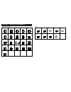
Section 9 semiconductor information • transistors and fet's • diodes 9 - 1 b e c b c e b e c b e c b e c b e c b e c g d s s d g b e c b e c d s g2 g1 g1 g2 s d b e c b e c e1 c2 b1 c1 e2 b2 e1 b1 b2 c1 c2 e1 b2 e2 c1 c2 b1 e1 e2 b2 c1 b1 c2 g s d s s d g g s d 2sa1577 t106 r 2sb1132 t100 r 2sc4081 ...
Page 29
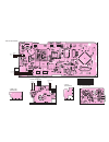
H5 h10 h15 h20 h25 h30 h35 h40 h45 h50 h55 h60 h65 h70 h75 h80 h85 h90 h95 h100 h105 h0 v5 v10 v15 v0 v25 v30 v35 v20 v45 v40 to speaker “sp1” (chassis) j4 4 2 3 1 sp gnd gnd gnd top switch mic 7 4 1 p0 p1 p2 p3 0 8 5 2 # 9 6 3 section 10 board layouts 10 - 1 • bc-160 (top view) • ant unit (top view...
Page 30
H5 h10 h15 h20 h25 h30 h35 h40 h45 h50 h55 h60 h65 h70 h75 h80 h85 h90 h95 h100 h105 h0 v5 v10 v15 v0 v25 v30 v35 v20 v45 v40 20 1 21 40 j5 opv1 opv2 opv3 gnd opt3 opt2 opt1 sigo bu s y nc bref nc dmi mcin dmo mco t ptt o ptti gnd d_if gnd cck csi cso nc cirq css rem da f o afout disc rmut bepo afon...
Page 31
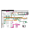
Section 11 block diagram 11 - 1 explanatory notes +b line lpf ic6 lm2902pwr lpf lpf dtmf encode ic6 lm2902pwr lpf ic7 njm12902v reset ic8 bd5242g shift sw d6 ma2s077 ant sw current det d701: 1sv307 d704: 1sv307 d706: 1sv307 pwr amp q701 rd07mvs1 tx/rx sw d16:1sv307 d17: ma2s077 rx vco q17 2sc5006 tx...
Page 32
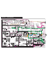
Section 12 voltage diagrams 12 - 1 %xplanatory 6/,4!'% 48 28 #/--/. # # # p # p # # $ 36 # , m( # # # p # , m ( # # p # # p # p # # p # p # p 2 k 2 k # p # # # p # p # p 8 #$"##8 # # p # p # # p # # # p # # # # p # # # # p # p # p # # # # p # # # # $ -!3 $ -!3 #42, '.$ ." 6/ 5 4 6). # # # # # # # # ...
Page 33
12 - 2 explanatory notes voltage line tx line rx line common line c707 0.001 c703 47p c702 100p r714 0.15 l901 blm21p300s l703 7.5nh c734 0.001 d702 rb706f-40 r706 4.7k c723 0.001 c759 0.001 c718 0.001 r703 4.7k c754 0.001 d703 rb706f-40 r726 4.7k r710 4.7k r709 22k c701 0.001 c742 0.001 r704 22 q70...
Page 34
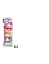
Section 13 bc-160 13 - 1 q1 2sc4081 r4 10 r18 r3 560 r5 0.12 r35 r31 10k r37 120k r28 r38 r29 1ss355 d2 d5 1ss355 c6 10 c11 0.01 c12 0.01 c8 0.01 c25 c26 c21 c22 0.1 0.01 c28 c23 c24 10k 0.1 0.01 0.01 c27 1k 39k 0.01 0.01 0.01 c1 0.001 0.01 c3 d4 d an202k c19 c16 r17 10k r16 560k r15 c18 56k 0.01 r1...
Page 35
6f no.68, sec. 1 cheng-teh road, taipei, taiwan, r.O.C. Phone : +886 (02) 2559 1899 fax : +886 (02) 2559 1874 url : http://www.Asia-icom.Com e-mail : sales@asia-icom.Com zac de la plaine, 1, rue brindejonc des moulinais bp 5804, 31505 toulouse cedex, france phone : +33 (5) 61 36 03 03 fax : +33 (5) ...
Page 36
1-1-32, kamiminami, hirano-ku, osaka 547-0003, japan s-14303hz-c1 © 2006 icom inc..

