- DL manuals
- Icom
- Transceiver
- IC-F4029SDR
- Service Manual
Icom IC-F4029SDR Service Manual
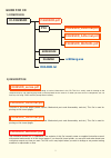
GUIDE FOR CD
1) COMPOSION
1
IC-F4029SDR
F4029SDR.pdf
FYC
ADDENDUM
Installer
ar505eng.exe
README.txt
2) DESCRIPTION
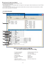
The service manual for IC-F4029SDR including all service information in this CD. This file is mainly used for viewing on the
computer display and checking page order to make printed service manual. Or when you want to find a component, you can
find very fast using “FIND” function (except Board Layouts).
Consists of A3 format pages (Board layouts, Mechanical parts and disassembly, and etc.). This file is used for
printing out A3 format pages.
Consists of A4 format pages (Board layouts, Mechanical parts and disassembly, and etc.). This file is used for
printing out A4 format pages.
The instruction manual for IC-F4029SDR. The contents of this file is exactly same as supplied instruction manual
with product and consists of all A4 format pages. If you have A4 format printer, you can print and make brand new
instruction manual any time you want. This file is also very helpful when you want to change or set product setting
condition for adjustment or else.
Summary of IC-F4029SDR
Page 1
Guide for cd 1) composion 1 ic-f4029sdr f4029sdr.Pdf fyc f4029sdr_a3format.Pdf f4029sdr_a4format.Pdf f4029sdr_manual.Pdf addendum installer ar505eng.Exe readme.Txt 2) description f4029sdr_series.Pdf the service manual for ic-f4029sdr including all service information in this cd. This file is mainly ...
Page 2: Ar505Eng.Exe
2 ========================================================================================= icom, icom inc. And icom logo are registered trademarks of icom incorporated (japan) in the united states, the united kingdom, germany, france, spain, russia and/or other countries. Adobe acrobat reader copyr...
Page 3: Service Manual
Service manual addendum contents parts list. . . . . . . . . . . . . . . . . . . . . . . . . . . . . . . . . . . . . . . . . 1 board layouts. . . . . . . . . . . . . . . . . . . . . . . . . . . . . . . . . . . . 7 voltage diagram . . . . . . . . . . . . . . . . . . . . . . . . . . . . . . . . . . 9 ...
Page 4: Parts
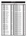
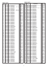
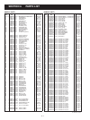
1 parts list m.=mounted side (t: mounted on the top side, b: mounted on the bottom side) [main-c unit] ref order description m. H/v no. No. Location ic2 1140005991 s.Ic mb15a02pfv1-g-bnd-ere1 t 81.2/34.5 ic3 1130011770 s.Ic cd4066bpwr b 40.4/22 ic5 1110005320 s.Ic njm13403v-te1 b 40.4/12.8 ic6 11100...
Page 5
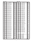
2 m.=mounted side (t: mounted on the top side, b: mounted on the bottom side) s.=surface mount [main-c unit] ref order description m. H/v no. No. Location r98 7030007290 s.Res erj2gej 222 x (2.2 k ) b 99/22.1 r100 7030005040 s.Res erj2gej 472 x (4.7 k ) t 74.4/22.5 r101 7030004990 s.Res erj2gej 221 ...
Page 6
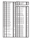
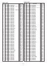
3 m.=mounted side (t: mounted on the top side, b: mounted on the bottom side) s.=surface mount [main-c unit] ref order description m. H/v no. No. Location c32 4030017460 s.Cer ecj0eb1e102k b 91/35.2 c33 4030017420 s.Cer ecj0ec1h470j b 90/35.2 c36 4030017460 s.Cer ecj0eb1e102k b 86.8/35.3 c39 4030017...
Page 7
4 m.=mounted side (t: mounted on the top side, b: mounted on the bottom side) s.=surface mount [main-c unit] ref order description m. H/v no. No. Location c332 4030017460 s.Cer ecj0eb1e102k t 80.5/4.6 c333 4550006250 s.Tan teesva 1a 106m8r t 83.1/3.4 c334 4030016930 s.Cer ecj0eb1a104k t 76.3/8.5 c33...
Page 8
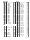
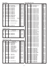
5 m.=mounted side (t: mounted on the top side, b: mounted on the bottom side) s.=surface mount [pa-c unit] ref order description m. H/v no. No. Location c747 4030017530 s.Cer ecj0ec1h0r5b t 34.4/12.9 c748 4030017360 s.Cer ecj0ec1h030b t 34.5/10 c750 4030006990 s.Cer c1608 ch 1h 080d-t b 30.4/14 c751...
Page 9
6 m.=mounted side (t: mounted on the top side, b: mounted on the bottom side) s.=surface mount [dsp unit] (ut-119s) ref order description m. H/v no. No. Location c37 4030017750 s.Cer ecj0eb1e122k b 26.3/12.8 c40 4030017420 s.Cer ecj0ec1h470j b 26.2/19.2 c41 4030017420 s.Cer ecj0ec1h470j b 25.4/18.3 ...
Page 10: Section 9
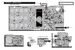
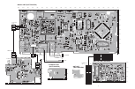
7 section 9 board layouts ( ( ( ( ( ( ( ( ( ( ( ( ( ( ( ( ( ( ( ( ( ( 6 6 6 6 6 6 6 6 6 6 ( ( ( ( ( ( ( ( 6 6 6 6 6 ( ( ( ( 6 6 6 ( ( ( ( ( ( ( ( 6 6 6 6 6 6 30%!+%2 h30v#(!33)3 4/0 37)4#( !.4%..! '.$ "!44 s-!).#5.)44/06)%7 s0!#5.)44/06)%7 s#/..%#45.)44/06)%7 s!.45.)4 4/06)%7 s$305.)44/06)%7 4he com...
Page 11
8 ( ( ( ( ( ( ( ( ( ( ( ( ( ( ( ( ( ( ( ( ( ( 6 6 6 6 6 6 6 6 6 6 ( ( ( ( ( ( ( ( 6 6 6 6 6 6 ( ( ( ( 6 6 6 ( ( ( ( ( ( ( ( 6 6 6 6 6 s-!).#5.)4"/44/-6)%7 s0!#5.)4"/44/-6)%7 s#/..%#45.)4 "/44/-6)%7 s!.45.)4 "/44/-6)%7 s$305.)4"/44/-6)%7 to0!#5nit h*v 28 '.$ !0# )3%.3 to-!).#5nit 620ower3witch %84-)#...
Page 12: Voltage
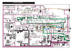
9 voltage diagram %xplanatorynotes 6/,4!'%,).% 48,).% 28,).% #/--/.,).% # # # p # p # # $ -! # , ( # # # p # , ( # # p # # p # p # p # # # p # p # p # 8 #$"##8 # # p # # p # # # p # # # # p # # # # p # p # # p # # # # p # # # # , n( $ -!3 #42, '.$ ." 6 /54 6). # # # # # # # # # # # $ -!3 -# 3+" # # ...
Page 13: �������
ic-f4029sdr s-14228mz-c1 apr. 2006 uhf transceiver.
Page 14
This service manual describes the latest service information for the ic-f4029sdr uhf transceiver at the time of publication. Be sure to include the following four points when ordering replacement parts: 1. 10-digit icom parts numbers 2. Component name and informations 3. Equipment model name and uni...
Page 15
Table of contents section 1 specifications section 2 inside views section 3 disassembly instructions section 4 circuit descripiton 4-1 receiver circuits. . . . . . . . . . . . . . . . . . . . . . . . . . . . . . . . . . . . . . . . . . . . . . . . . . . . . . . . 4-1 4-2 transmitter circuits . . . ....
Page 16: Section 1
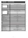
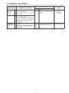
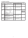
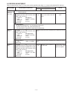
1 - 1 section 1 specifications general • frequency coverage 446.00625–446.09375 mhz (analog) 446.103125–446.196875 mhz (digital) • type of emission wide 16k0f3e (25.0 khz) middle 14k0f3e (20.0 khz) narrow 8k50f3e (12.5 khz) digital 4k00f1d (6.25 khz) • number of programable channels 64 channels (4 z...
Page 17
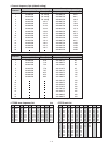
1 - 2 & & & & & & & & & & ' ' ' ' ' ' ' ' ' ' ( ( ( ( ( ( ( ( ( ( ) ) ) ) #ode .O ! ! ! ! ! ! ! ! ! ! &req .O " " " " " " " " " " &req .O # # # # # # # # # # &req .O $ $ $ $ $ $ $ $ $ $ &req .O % % % % % % % % % % :one!Nalogmode &requency-(z 4one(z . . . . :one!Nalogmode &requency-(z 4one(z .Osettin...
Page 18: Section 2
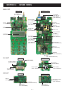
2 - 1 section 2 inside views ...
Page 19: Section 3
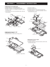
3 - 1 section 3 disassembly instructions 2 removing the main-c unit q remove the main seal f . W unscrew vr nut g , and remove the top plate h . 3 removing the pa-c unit q unscrew 3 screws m . W unsolder 4 points n , and take off the pa-c unit in the direction of the arrow. 1 removing the chassis un...
Page 20: Section 4
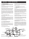
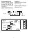
Section 4 circuit description 4-1 receiver circuits 4-1-1 antenna switching circuit (pa-c unit) the antenna switching circuit toggles the receive (rx) line and transmit (tx) line. The received signals from the antenna are passed through the low-pass filter (lpf; l709, l710, c742, c744−c748) and ante...
Page 21
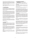
The af signal from the analog switch (ic3, pin 11) are applied to the volume buffer amplifi er (ic6, pin 9). The buffer- amplifi ed af signals are adjusted its level (=audio level) by volume control pot (r315), then applied to the af power amplifier (ic15, pin 4) and amplified to the 0.5 w of audio ...
Page 22
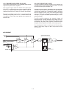
4-2-3 transmit amplifiers (pa-c unit) the transmit signal from the vco is amplifi ed to the transmit output level by the transmit amplifi ers. The transmit signal from the tx/rx switch (d16=on, d17=off) is amplified by two pre-drive amplifiers (q703, q704), drive amplifi er (q702) and power amplifi ...
Page 23
Loop filter rx vco q16, d10, d13 q17, d9, d10 tx vco pll control signals from the cpu (ic22) pll unlock signal to the cpu (ic22, pin 34) 15.3 mhz reference frequency signal • pll circuit buffer buffer ×2 to transmitter circuits to 1st if circuits d17 d16 bpf plst sso sck 5 7 8 1 9 10 11 pll ic (ic2)...
Page 24
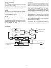
4 - 5 cpu5v regurator +5v regurator s5v regurator t5v regurator r5v regurator power switch r315 f701 (pa-c unit) q26–q28 ic17 q23 q24, q49 q25 vcc cpu5 cpu +5v s5v “s5c” “pwon” voltage line control signal 8 22 87 88 “t5c” “r5c” t5v led backlight driver (q45), lcd driver (ic20), d/a converter (ic12),...
Page 25
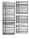
4 - 6 4-6-1 cpu ( ic22) pin no. Port name description 1−3 kr1− kr3 input ports for dealer-programmable keys. 4−8 ks0− ks4 output ports for dealer-programmable keys. 9 busy outputs “busy” signal to the dsp unit. 10 ccs outputs chip-select signal to the dsp unit. 11 sck outputs serial clock signal to ...
Page 26: Section 5
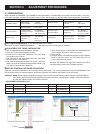
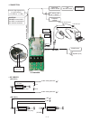
Section 5 adjustment procedures 5-1 preparation when adjusting ic-f4029sdr, cs-f4029dr cloning software, cs-f4029 adj adjustment software (rev. 1.0 or later), opc-478/u jig cable (modifi ed opc-478/u cloning cable ; see the page 5-2) and the following test equipments are required. Equipment grade an...
Page 27
5 - 2 ic-f4029sdr fm deviation meter osciiloscope to the j701 (p a-c unit) attenuator 10 db or 20 db rf power meter 0.01–1 w/50 Ω frequency counter standard signal generator 0.1 µv to 32 mv (–127 dbm to –17 dbm) caution! Do not transmit while the ssg is connected to the antenna connector sinad meter...
Page 28
5 - 3 reference frequency receive sensitivity (manually) pll lock voltage preset s-meter mode preset reload data pll lock voltage (verify) squelch ctcss/dtcs deviation fm deviation digital deviation modulation balance transmit output power tq pll lock voltage w e r t y u i o !0 !1 !3 q w e r t y u i...
Page 29
5 - 4 5-2 frequency adjustment select an adjustment item using [ ↑ ] / [ ↓ ] keys, then set to the specifi ed value using [ ← ] / [ → ] keys on the connected pc’s keyboard. Adjustment adjustment condition measurement value unit operation pll lock voltage [rx lva] 1 • channel • lock voltage preset [l...
Page 30
5 - 5 5-3 transmit adjustment select an adjustment item using [ ↑ ] / [ ↓ ] keys, then set to the specifi ed value using [ ← ] / [ → ] keys on the connected pc’s keyboard. Adjustment adjustment condition measurement value unit operation transmit output power [power (hi)] 1 • channel • transmitting :...
Page 31
5 - 6 5-4 receive adjustment select an adjustment item using [ ↑ ] / [ ↓ ] keys, then set to the specifi ed value using [ ← ] / [ → ] keys on the connected pc’s keyboard. Adjustment adjustment condition measurement value unit location receive sensitivity [bpf (t1)] [bpf (t2)] note: “receive sensitiv...
Page 32: Section 6
6 - 1 section 6 parts list m.=mounted side (t: mounted on the top side, b: mounted on the bottom side) [main-c unit] ref order description m. H/v no. No. Location ic2 1140005991 s.Ic mb15a02pfv1-g-bnd-ere1 t 81.2/34.5 ic3 1130011770 s.Ic cd4066bpwr b 40.4/22 ic5 1110005320 s.Ic njm13403v-te1 b 40.4/...
Page 33
6 - 2 m.=mounted side (t: mounted on the top side, b: mounted on the bottom side) s.=surface mount [main-c unit] ref order description m. H/v no. No. Location r98 7030007290 s.Res erj2gej 222 x (2.2 k ) b 99/22.1 r100 7030005040 s.Res erj2gej 472 x (4.7 k ) t 74.4/22.5 r101 7030004990 s.Res erj2gej ...
Page 34
6 - 3 m.=mounted side (t: mounted on the top side, b: mounted on the bottom side) s.=surface mount [main-c unit] ref order description m. H/v no. No. Location c32 4030017460 s.Cer ecj0eb1e102k b 91/35.2 c33 4030017420 s.Cer ecj0ec1h470j b 90/35.2 c36 4030017460 s.Cer ecj0eb1e102k b 86.8/35.3 c39 403...
Page 35
6 - 4 m.=mounted side (t: mounted on the top side, b: mounted on the bottom side) s.=surface mount [main-c unit] ref order description m. H/v no. No. Location c332 4030017460 s.Cer ecj0eb1e102k t 80.5/4.6 c333 4550006250 s.Tan teesva 1a 106m8r t 83.1/3.4 c334 4030016930 s.Cer ecj0eb1a104k t 76.3/8.5...
Page 36
6 - 5 m.=mounted side (t: mounted on the top side, b: mounted on the bottom side) s.=surface mount [pa-c unit] ref order description m. H/v no. No. Location c747 4030017530 s.Cer ecj0ec1h0r5b t 34.4/12.9 c748 4030017360 s.Cer ecj0ec1h030b t 34.5/10 c750 4030006990 s.Cer c1608 ch 1h 080d-t b 30.4/14 ...
Page 37
6 - 6 m.=mounted side (t: mounted on the top side, b: mounted on the bottom side) s.=surface mount [dsp unit] (ut-119s) ref order description m. H/v no. No. Location c37 4030017750 s.Cer ecj0eb1e122k b 26.3/12.8 c40 4030017420 s.Cer ecj0ec1h470j b 26.2/19.2 c41 4030017420 s.Cer ecj0ec1h470j b 25.4/1...
Page 38: Section 7
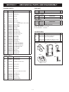
7 - 1 section 7 mechanical parts and disassembly screw abbreviations b0, bt: self-tapping ph: pan head ni-zu: nickel-zinc zk: black [main-c unit] ref. No. Order no. Description qty. Ep1 optional product ac adapter bc-147e 1 ep2 optional product li-ion battery pack bp-231 1 ep3 optional product batte...
Page 39
7 - 2 ...
Page 40: Section
Name symbol inside view 1sv307 tx dan222 n hvc350b-e b0 ma2s077 ma2s111 ma2s728 s a b ma368 6l rb706f-40 3j name symbol inside view dta114eu unr9111j unr9113j 16 6a 6c rd01mus1 k2 g s d g s d rd07mvs1 rd07mvs1 s d g g s d unr9213j 8c xp1214 9h xp4601 5c ...
Page 41: Section 9
9 - 1 section 9 board layouts ...
Page 42
9 - 2 ...
Page 43
10 - 1 section 10 block diagram ...
Page 44
11 - 1 section 11 voltage diagram ...
Page 45: ���������
11 - 2 ...
Page 46
1 n o i t c e s 2 0 6 1 - c b 12 1 - 1 q 1 8 0 4 c s 2 4 r 0 1 r18 r3 560 5 r 2 1 . 0 r35 1 3 r k 0 1 r37 120k 8 2 r r38 r29 5 5 3 s s 1 2 d d5 1ss355 c 6 10 c11 0.01 c12 0.01 c 8 0.01 c25 c26 c21 c22 0.1 0.01 c28 c23 c24 10k 0.1 0.01 0.01 c27 1k 39k 0.01 0.01 0.01 c1 0.001 0.01 c3 d4 d an202k c19 c...
Page 47
6f no.68, sec. 1 cheng-teh road, taipei, taiwan, r.O.C. Phone : +886 (02) 2559 1899 fax : +886 (02) 2559 1874 url : http://www.Asia-icom.Com e-mail : sales@asia-icom.Com zac de la plaine, 1, rue brindejonc des moulinais bp 5804, 31505 toulouse cedex, france phone : +33 (5) 61 36 03 03 fax : +33 (5) ...
Page 48
1-1-32, kamiminami, hirano-ku, osaka 547-0003, japan s-14228mz-c1 © 2006 icom inc..

