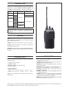
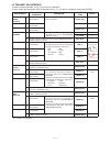
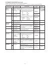
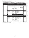
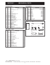
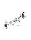
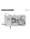
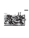
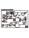
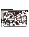
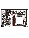
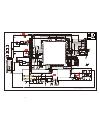
Summary of IC-F4101D
Page 1
S-14801xz-c1 apr. 2011 uhf transceivers.
Page 2
This service manual describes the latest technical information for the ic- f4101d, ic-f4102d, ic-f4103d and ic-f4106d uhf transceivers , at the time of publication. Never connect the transceiver to an ac outlet or to a dc power supply that uses more than the specified voltage. This will ruin the tra...
Page 3
Table of contents section 1 specifications section 2 inside views section 3 disassembly instruction section 4 circuit descripiton 4-1 receiver circuits. . . . . . . . . . . . . . . . . . . . . . . . . . . . . . . . . . . . . . . . . . . . . . . . . . . . . . . . 4-1 4-2 transmitter circuits . . . . ...
Page 4: Section 1. Specifications
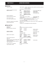
1 - 1 section 1. Specifications m general • frequency range : 400–470 mhz [usa-01], [eur-01], [uk-01], [exp-01], [exp-02], [exp-03], [aus-01], [rus-01] 350–400 mhz [exp-07], [exp-08] • number of conventional channels : 16 • type of emission : wide 16k0f3e (30.0 khz) except [usa], [eur], [uk] 16k0f3e...
Page 5
1 - 2 m receiver • sensitivity : 0.24 µv typ. At 12 db sinad except [eur], [uk] –4 dbµv (emf) typ. At 20 db sinad [eur], [uk] –8 dbµv (emf) typ. At 5% ber [digital mode] • squelch sensitivity (at threshold) : 0.20 µv typ. Except [eur], [uk] –8 dbµv (emf) typ. [eur], [uk] • intermediate frequency : 1...
Page 6: Section 2. Inside
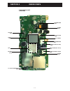
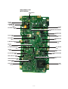
2 - 1 section 2. Inside views • main-a/main-c unit (top view) vco 5 v regulator (ic54) pll circuit apc amp (ic1) tcxo (x2) 3.3 v dc-dc converter (ic65) mic amp (ic64) 2nd if filter (for wide) (fi3) 1st if filter (fi2) discriminator (x1) 2nd if filter (for narrow) (fi4) 2nd if filter (for digital) (f...
Page 7
2 - 2 • main-a/main-c unit (bottom view) tx power amp (q1) buffer (q28) pll lock voltage sw (ic6) clock amp (ic905) 2nd if amp (for digital) (ic5) af power amp sw (q64) drive amp (q2) pre-drive amp (q3) pre amp (q4) rf amp (q22) rf amp gate bias control (q21) af amp (ic55) if demodulator ic (ic3) bu...
Page 8: Section 3. Disassembly
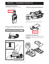
3 - 1 section 3. Disassembly instruction 3 - 1 be careful to not pull out the speaker wire when separating the chassis and the front panel. For easy separation of the chassis use a suction lifter to lift the bottom of the chassis up. 1. Removing the chassis 1) remove the ant connector nut and 2 knob...
Page 9: Section 4. Circuit
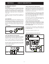
4 - 1 section 4. Circuit description 4-1 receiver circuits rf circuits the rx signal from the antenna is passed through the lpf and antenna sw (d3, d22), then filtered by the 2-staged tuned bpf (d24 and d26) to eliminate unwanted out-of- band signals. The filtered rx signal is amplified by the rf am...
Page 10
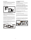
4 - 2 rx af circuits the demodulated af signal from the linear codec (ic902) is passed through the lpf (ic60c), and then adjusted in level by the d/a converter (ic57). The level-adjusted af signal is then amplifi ed by af amps (ic58 and ic55). The amplifi ed af signal is applied to the internal or e...
Page 11
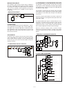
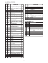
4 - 3 modulation circuit the modulation signal from the tx af circuits is applied to d15 of the tx vco (q14, d14–d16) to modulate it (fm for the analog mode, 4fsk for the digital mode). The modulated signal from the tx vco is buffer-amplified by two buffers (q8, q10), and applied to the tx amp circu...
Page 12
4 - 4 4-5 port allocations • cpu (ic51) • d/a converter (ic57) pin no. Line name description 3 bal dtcs balance adjustment. 4 afvo af volume adjustment. 12 tenc outputs ctcss deviation adjustment. 15 sqlc squelch threshold setting. 16 t1 during rx: outputs bpf tuning voltage. During tx: outputs tx p...
Page 13: Section 5. Adjustment
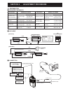
5 - 1 section 5. Adjustment procedure ¤ jig cable equipment grade and range equipment grade and range cloning software cs-f3100d/f5120d (revision 1.0 or later) jig cable modifi ed opc-478uc (see the illust below) rf power meter (50 Ω terminated) measuring range : 0.1–10 w frequency range : 100–600 m...
Page 14
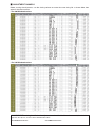
5 - 2 convenient: the cloning data fi le for the adjustment, as described in this service manual, is attached. Right click the clip icon, and select "save embeded file to disk." • for 400 mhz band versions: • for 350 mhz band versions: ¤ adjustment channels • for 350 mhz band versions • for 400 mhz ...
Page 15
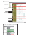
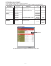
S-meter digital deviation 2/5 tone deviation 5 - 3 ¤ adjustment utility adjustment condition reference frequency tx output power fm deviation squelch sensitivity pll lock voltage ctcss deviation dtcs deviation modulation balance for [eur] versions: when adjusting “deviation” in the middle band, chan...
Page 16
5 - 4 adjustment transceiver’s condition operation adjustment item value pll lock voltage -rx- (band low) 1 • channel : 1-1 • receiving 1) connect an rf power meter to the antenna connector. 2) set the preset adjustment value on the adjustment utility window. [rx lva(adjust)] 1.00 v (band high) 2 • ...
Page 17
5 - 5 adjustment transceiver’s condition operation adjustment item value tx output power (hi power) 1 • channel : 1-4 • transmitting • connect an rf power meter to the an- tenna connector. [power (hi)] 4.0 w (l2 power) 2 • channel : 1-5 • transmitting [power (l2)] 2.0 w (l1 power) 3 • channel : 1-6 ...
Page 18
5 - 6 5-3 transmit adjustments (continued) 1) select an adjustment item using [ ↑]/[↓] on the pc's keyboard. 2) set or modify the adjustment value as specifi ed using [ ←]/[→] on the pc's keyboard, then push [enter]. Adjustment transceiver’s condition operation adjustment item value fm deviation -mi...
Page 19
5 - 7 adjustment transceiver’s condition operation adjustment item value receive sensitivity note: “receive sensitivity” must be adjusted before “s-meter.” otherwise, “s-meter” will not beadjusted properly. When “receive sensitivity” is re-adjusted, “s-meter” must be also re-adjusted. 1 • channel : ...
Page 20: Section 6. Parts
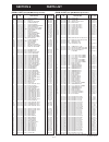
6 - 1 section 6. Parts list ic1 1110002751 s.Ic ta75s01f(te85rf) t 32.5/8.9 ic3 1110007320 s.Ic njm2591v-te1-#zzzb b 45.8/38.9 ic4 1130015270 s.Ic ak1541p-l t 43.2/24.0 ic5 1110006230 s.Ic njm2711f-te1-#zzzb b 68.3/44.2 ic6 1130011741 s.Ic tc7w66fk(te85lf) b 65.3/26.7 ic21 1110002751 s.Ic ta75s01f(t...
Page 21
6 - 2 ref parts description m. H/v no. No. Location [main-a unit] (for [400 mhz band] versions) r45 7030004980 s.Res erj2gej 101 x (100) t 63.2/17.9 r46 7030005090 s.Res erj2gej 104 x (100k) t 62.8/19.3 r51 7030005000 s.Res erj2gej 471 x (470) b 54.5/24.5 r52 7030005000 s.Res erj2gej 471 x (470) b 6...
Page 22
6 - 3 ref parts description m. H/v no. No. Location [main-a unit] (for [400 mhz band] versions) r632 7030005050 s.Res erj2gej 103 x (10k) b 82.9/23.1 r633 7030005040 s.Res erj2gej 472 x (4.7k) b 85.7/21.9 r634 7030005050 s.Res erj2gej 103 x (10k) t 82.7/11.4 r635 7030005050 s.Res erj2gej 103 x (10k)...
Page 23
6 - 4 ref parts description m. H/v no. No. Location [main-a unit] (for [400 mhz band] versions) c171 4030017570 s.Cer c1005 ch 1h 040b-t b 15.3/16.0 c172 4030017350 s.Cer c1005 ch 1h 020b-t b 15.3/17.2 c173 4030017460 s.Cer c1005 jb 1h 102k-t b 13.9/18.8 c175 4030017420 s.Cer c1005 ch 1h 470j-t b 13...
Page 24
6 - 5 ref parts description m. H/v no. No. Location [main-a unit] (for [400 mhz band] versions) c904 4050000240 s.Fee nfm18pc104r1c3d b 73.1/41.2 c905 4050000240 s.Fee nfm18pc104r1c3d b 72.3/36.9 c907 4030017460 s.Cer c1005 jb 1h 102k-t t 75.2/32.3 c908 4030018910 s.Cer c1608 jb 0j 475k-t t 77.5/34....
Page 25
6 - 6 ref parts description m. H/v no. No. Location [main-c unit] (for [350 mhz band] versions) d55 1750001810 s.Dio l1ss400t1g b 22.8/34.9 d59 1750001850 s.Dio ldan222t1g b 4.2/37.5 d60 1750001790 s.Dio 1ss390 te61 b 85.0/23.6 d901 1790001241 s.Dio ma2s7280gl t 87.1/27.9 d902 1790001241 s.Dio ma2s7...
Page 26
6 - 7 ref parts description m. H/v no. No. Location [main-c unit] (for [350 mhz band] versions) r365 7030005040 s.Res erj2gej 472 x (4.7k) b 26.2/38.9 r366 7030005100 s.Res erj2gej 154 x (150k) b 57.8/12.4 r367 7030005600 s.Res erj2gej 273 x (27k) t 53.6/2.2 r368 7030005700 s.Res erj2gej 274 x (270k...
Page 27
6 - 8 ref parts description m. H/v no. No. Location [main-c unit] (for [350 mhz band] versions) c37 4030017720 s.Cer c1005 jb 1h 331k-t b 24.7/16.1 c38 4030017460 s.Cer c1005 jb 1h 102k-t b 32.7/15.1 c39 4030017420 s.Cer c1005 ch 1h 470j-t b 32.7/14.1 c45 4030017500 s.Cer c1005 ch 1h 560j-t b 32.7/1...
Page 28
6 - 9 ref parts description m. H/v no. No. Location [main-c unit] (for [350 mhz band] versions) c381 4030016930 s.Cer c1005 jb 1a 104k-t t 68.0/4.5 c382 4030016930 s.Cer c1005 jb 1a 104k-t t 66.4/4.5 c383 4030018860 s.Cer c1005 jb 0j 105k-t t 64.8/4.5 c384 4030018860 s.Cer c1005 jb 0j 105k-t t 63.2/...
Page 29: Section 7. Mechanical
7 - 1 [chassis parts] ref order description qty. No. No. Ep1* 0910067870 b7261 ant j1 6910021491 ant connector 106-1 1 sp1 2510001560 045p01202-02 1 w1 8900009640 opc-963 1 mp1 8010022041 3286 chassis-1 2x2 1 mp2 8210026490 3328 front panelassembly 1 mp10 8930082160 3285 name sheet (a) 1 mp11 893008...
Page 30
7 - 2 mp10(c) mp18(c) mp33(c) s54(m) mp16(c) mp11(c) mp12(c) mp24(c) mp27(c) mp25(c) sp1(c) mp2(c) mp1(c) mp23(c) mp22(c) ep1(c) j1(c) mp13(c) mc51(m) mp2(m) mp34(c) mp34(c) mp35(c) mp32(c) mp32(c) j52(m) j51(m) mp21(c) s51(m) mp20(c) mp31(c) mp31(c) mp19(c) mp14(c) mp17(c) r421(m) mp15(c) w1(c) abb...
Page 31
8 - 1 section 8. Board layouts • main-a/main-c unit (top view) the combination of this page and next page shows the top side and bottom side of actual p.C. Board. [mic] antenna connector ep1 (chassis) j1 (chassis) [sp] sp+ 1 sp− 2 sp1 (chassis) j53 mp10 mp13 mp14 mp7 mp3 mp6 mp8 mp12 c26 c27 c28 c30...
Page 32
8 - 2 the combination of this page and next page shows the top side and bottom side of actual p.C. Board. • main-a/main-c unit (bottom view) j51 j52 [vol] [ptt] [upper] [lower] [rotary selector] c1 c2 c3 c4 c5 c6 c7 c8 c9 c10 c11 c12 c13 c14 c15 c18 c19 c35 c36 c37 c38 c39 c45 c47 c48 c49 c51 c52 c5...
Page 33
9 - 1 section 9. Block diagram lpf lpf shift sw d60 1ss390 ant sw d22:hvd142a d3:hvd142a pwr amp q1 rd07mus2b tx/rx sw d6:hvd142a d5:hvd142a q13 2sc4226 d12 hvd350b q14 2sc4226 d16 hvd350b fil ripple q15 2sc4116 fil loop pll ic ic4 ak1541 x3 q26 2sc4116 x1 jtbm450cx x51 cr-912 fm mod d15 1sv309 q23 ...
Page 34
10 - 1 section 10. Voltage diagram • main-a/c unit (1/3) tx 0.82v rx 0v tx 4w 2.26v tx 1w 0.98v rx 0v tx 1.66v rx 0v tx 4.89v rx 0v tx 4w 3.50v tx 1w 1.56v rx 0v tx 4w 1.76v tx 1w 1.25v rx 0v tx 0.70v rx 0v tx 1.34v rx 1.34v tx 1.99v rx 0v tx 0v rx 1.99v 7.50v 0.78v 0.76v 4.51v 4.98v 4.24v 0.77v tx ...
Page 35
10 - 2 • main-a/c unit (2/3) *: refer to the parts list for the value and name of component. Tx 0v rx 4.82v tx 4.89v rx 0v tx 0v rx 3.32v tx 3.32v rx 0v afon 5.27v off 0v 19.66mhz 1.73vp-p 2.23v 1.43v 3.28v 3.32v 5.00v c453 15p ic66 tc7w53fk 1 com 2 inh 3 vee 4 gnd 5 a 6 ch1 7 ch0 8 vcc r468 680 q90...
Page 36
10 - 3 • main-a/c unit (3/3) *: refer to the parts list for the value and name of component. 12.288mhz 1.14vp-p 1.43v 3.27v 1.58v 3.27v r916 47k c946 0.1 cp118 r958 100k c926 0.001 r930 47k c934 4.7 c920 0.01 c955 0.1 c918 0.01 c944 0.1 r972 0 c953 0.001 cp111 r909 100 c932 0.1 ic902 pcm3008t 1 vcom...
Page 37
6f no.68, sec. 1 cheng-teh road, taipei, taiwan, r.O.C. Phone : +886 (02) 2559 1899 fax : +886 (02) 2559 1874 url : http://www.Asia-icom.Com e-mail : sales@asia-icom.Com zac de la plaine 1 rue brindejonc des moulinais bp 5804 31505 toulouse cedex, france phone : +33 (5) 61 36 03 03 fax : +33 (5) 61 ...
Page 38
1-1-32, kamiminami, hirano-ku, osaka 547-0003, japan s-14801xz-c1 © 2011 icom inc..

