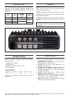
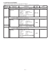
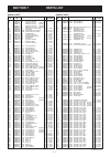
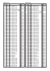
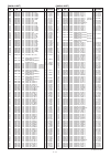
Summary of IC-F5011
Page 1
S-14712xz-c1 feb. 2011 vhf mobile transceivers.
Page 2
This service manual describes the latest technical information for the ic-f5011, ic-f5012, ic-f5013 and ic-f5013h vhf mobile transceiver, at the time of publication. Never connect the transceiver to an ac outlet or to a dc power supply that uses more than the specified voltage. This will ruin the tr...
Page 3
Table of contents section 1 specifications section 2 inside views section 3 disassembly instruction] section 4 optional products installation section 5 circuit descripiton 5-1 receiver circuits. . . . . . . . . . . . . . . . . . . . . . . . . . . . . . . . . . . . . . . . . . . . . . . . . . . . . ....
Page 4: Section 1. Specifications
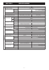
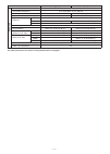
1 - 1 section 1. Specifications [usa], [exp] [eur] general • frequency coverage 136–174 mhz • type of emission wide 16k0f3e (25.0 khz) middle – 14k0f3e (20.0 khz) narrow 11k0f3e (12.5 khz) 8k50f3e (12.5 khz) • number of conventional channels 8 • antenna impedance 50 Ω (nominal) • operating temperatu...
Page 5
1 - 2 [usa], [exp] [eur] receiver • receive system double-conversion superheterodyne • intermediate frequencies 1st if; 46.35 mhz, 2nd if; 450 khz • sensitivity 0.25 μ v typ. At 12 db sinad −4 db μ v (emf) typ. At 20 db sinad • squelch sensitivity (at threshold) 0.25 μ v typ. −4 db μ v (emf) typ. • ...
Page 6: Section 2. Inside
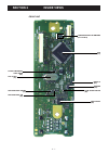
2 - 1 section 2. Inside views tx/rx indicator led drivers (q13 and q14) • front unit cpu (ic1) reset ic (ic2) eeprom (ic3) tone filter (ic5) tone filter switch (q3) clock frequency shift diode (d6) cpu clock (x1) key backlight sw (q2) key backlight driver (q1).
Page 7
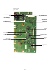
2 - 2 • main-a unit (top view) if demodulator ic (ic1) tone filetr (q39) pll ic (ic4) cpu5 line regulator (ic10) ripple filter (q17) vco switch (q15) vcc line switch (q23) +8v line regulator (ic9) r8 line regulator (q30) apc amp (ic2) 2nd if filter bandwidth switch (q40) 1st if filter (fi1) af amp (...
Page 8
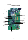
2 - 3 vco • main-a unit (bottom view) af/tone filter (ic16) af mute sw (q35) modulation line sw (q31) reference oscillator modulation buffer (ic19) d/a converter (ic18) reference frequency oscillator (x2) af amp (ic15) expander (ic17) af line sw (ic14) d/a converter (ic20) drive amp (q9) rf amp (q2)...
Page 9: Section 3. Disassembly
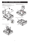
3 - 1 section 3. Disassembly instruction 1) remove 4 screws from the bottom cover, and then remove it. 2) disconnect the fl at cable and speaker cable. 3) remove 2 screws from the both sides, and then remove the front panel in the direction of the arrow. 4) remove 9 screws from the pcb. Flat cable b...
Page 10: Section 4
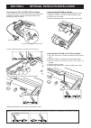
4 - 1 section 4 optional products installation install optional opc-1939/opc-2078 as follows: 1) turn off the power, and then disconnect the dc power cable. 2) remove 4 screws, and then remove the bottom cover. 3) install the cable as shown. Opc-1939/opc-2078 cut off the bushing as in the illustrati...
Page 11: Section 5. Circuit
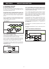
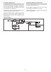
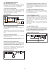
5 - 1 section 5. Circuit description 5-1 receiver circuits rf circuits (main-a unit) rf signal from the antenna is passed through the lpf (as the harmonic filter for transmitting) and antenna sw, and then applied to the rx bpf circuit. The applied rx signal is passed through the 2-staged tuned bpf (...
Page 12
5 - 2 lpf ic16 lpf ic16 lpf q39 hpf ic16 af amp ic15 af power amp ic8 am p ic21 af mute q35,36,d29 int. Speaker ext. Speaker jack j4 analog sw sdec to the cpu (front unit: ic1) cdec ic14 d/a ic18 (2/5 tone signals) (tcss/dtcs signals) front unit af on disc from the if ic disc disc vraf tmoni rxaf af...
Page 13
5 - 3 splat. Ic16 amp ic16 amp ic5 mic line sw mic d/a ic14 cd4066 ic18 microphone connector j1 front unit mic bal to the reference frequency oscillator modi mcot mcgo tone cdts mod vraf tx vco spin ref osc x2 cr-794 tx/rx sw d14,d15 q13,d16,31 fil loop pll ic ic4 mb15a02 fm mod d18 buff q10 buff q1...
Page 14
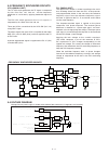
5 - 4 5-3 frequency synthsizer circuits vcos (main-a unit) the tx vco which generates the tx signal is composed by q13, d16, d31, l25, l38, etc., and the frequency modulation is carried out by applying modulation signals to d18. The rx vco which generates the 1st lo signals is composed by q14, d33, ...
Page 15
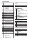
5 - 5 • cpu (front unit; ic1) pin no. Port name description i/o 1−3 kr1− kr3 dealer-programmable keys input. I 10 ccs chip-select signal to the attached optional unit. O 19− 21 cenc0− cenc2 ctcss/dtcs signal. O 23 duse frequency response of tone filter (ic5) switching control. “low”=while transmitti...
Page 16: Section 6. Adjustment
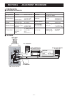
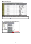
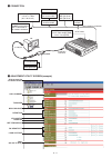
6 - 1 section 6. Adjustment procedure equipment grade and range equipment grade and range cloning software cs-f5010 : revision 1.0 or later jig cable modifi ed opc-1122u (see the illust below) dc power supply output voltage current capacity : 13.6 v dc except [eur] 13.2 v dc [eur] : more than 20 a a...
Page 17
6 - 2 m adjustment frequencies before starting adjustment, clone adjustment frequencies and settings into the transceiver as below. Select “middle” note: for [eur] versions, when adjust “deviation,” “modulation balance,” and “s-meter” in the middle band, change the bandwidth to “middle” as below. Co...
Page 18
6 - 3 m adjustment utility screen (example) m connection modulation analyzer (dc measurable) attenuator 50 db or 60 db to the antenna connector to dc cable standard signal generator –127 to –17 dbm (0.1 v to 32 mv) caution: do not transmit while ssg is connected to the antenna connector. Rf power me...
Page 19
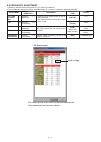
6 - 4 6-2 frequency adjustment 1) select an adjustment item using cursor or [ ↑ ]/[ ↓ ] of the pc’s keyboard. 2) set or modify the adjustment value as specifi ed using [ ← ]/[ → ] of the pc’s keyboard, then push [enter]. Adjustment transceiver’s condition operation adjustment item value pll lock vol...
Page 20
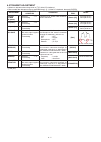
6 - 5 6-3 transmit adjustment 1) select an adjustment item using cursor or [ ↑ ]/[ ↓ ] of the pc’s keyboard. 2) set or modify the adjustment value as specifi ed using [ ← ]/[ → ] of the pc’s keyboard, then push [enter]. Adjustment transceiver’s condition operation adjustment item value output power ...
Page 21
6 - 6 6-4 receive adjustment 1) select an adjustment item using cursor or [ ↑ ]/[ ↓ ] of the pc’s keyboard. 2) set or modify the adjustment value as specifi ed using [ ← ]/[ → ] of the pc’s keyboard, then push [enter]. Adjustment transceiver’s condition operation adjustment item value receive sensit...
Page 22: Section 7. Parts
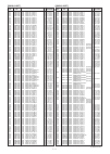
7 - 1 section 7. Parts list ic1 1110007320 s.Ic njm2591v-te1-#zzzb b 67.8/23 ic2 1110002751 s.Ic ta75s01f(te85rf) b 44.5/31.1 ic3 1150002372 ic ra30h1317m1-201 [eur-01] 1150002372 ic ra30h1317m1-201 [exp-01] 1150002423 ic ra60h1317m1a-222 [usa-01] 1150002423 ic ra60h1317m1a-222 [exp-02] ic4 11400059...
Page 23
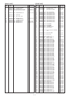
7 - 2 ref parts description m. H/v no. No. Location [main-a unit] r40 7030005030 s.Res erj2gej 152 x (1.5k) b 60.4/24.8 r41 7030010040 s.Res erj2gej-jpw t 60.2/17.8 r42 7030007340 s.Res erj2gej 153 x (15k) t 50.4/26.1 r43 7030005000 s.Res erj2gej 471 x (470) t 54.2/22.0 r44 7030005110 s.Res erj2gej ...
Page 24
7 - 3 ref parts description m. H/v no. No. Location [main-a unit] r357 7030005120 s.Res erj2gej 102 x (1k) t 114.9/7.1 r358 7030005120 s.Res erj2gej 102 x (1k) t 112.4/14.2 r359 7030005090 s.Res erj2gej 104 x (100k) t 111.5/9.4 r360 7030005090 s.Res erj2gej 104 x (100k) b 112.4/8.4 r361 7030005090 s...
Page 25
7 - 4 ref parts description m. H/v no. No. Location [main-a unit] c180 4550006970 s.Tan teesva0g476m8r t 35.9/30.3 c181 4030016930 s.Cer c1005 jb 1a 104k-t b 29.8/19.3 c182 4030016790 s.Cer c1005 jb 1e 103k-t b 28.5/19.6 c183 4030016930 s.Cer c1005 jb 1a 104k-t b 27.6/18.0 c184 4030017700 s.Cer c100...
Page 26
7 - 5 ref parts description m. H/v no. No. Location [main-a unit] j1 6510026770 s.Con axk540147yg t 23.0/8.3 j2 6510027960 s.Con 04-6294-040-000-800 t 67.5/10.6 j4 6450000140 con hsj0807-01-010 j6 6510022891 s.Con b13b-zr-sm4-tf(lf)(sn) t 120.0/17.2 j7 6510014961 s.Con b2b-zr-sm4-tf(lf)(sn) t 130.5/...
Page 27
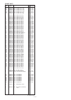
7 - 6 ref parts description m. H/v no. No. Location [front unit] r133 7030008400 s.Res erj2gej 182 x (1.8k) b 40.5/20.7 r134 7030008400 s.Res erj2gej 182 x (1.8k) b 57.6/21.4 r135 7030005030 s.Res erj2gej 152 x (1.5k) b 27.4/28.4 r136 7030005030 s.Res erj2gej 152 x (1.5k) b 47.2/28.3 r137 7030005030...
Page 28: Section 8. Mechanical
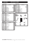
8 - 1 [chassis parts] ref order description qty. No. No. J1 6510004880 mr-ds-e 01 1 w1 8900011800 opc-1199 1 mp1 8010019065 2601 chassis-5 [eur-01] 1 8010019065 2601 chassis-5 [exp-01] 1 8010019135 2601 long chassis-5 [usa-01] 1 8010019135 2601 long chassis-5 [exp-02] 1 mp2 8110007821 2601 cover-1 r...
Page 29
8 - 2 mp8 (c)×2 r14 (f) j1 (f) w1 (f) mp7 (f)×2 mp10 (f) front unit unit abbreviations ( f): front unit (m): main-a unit (c): chassis parts mp4 (f) mp3 (f) mp5 (f) mp11 (f) mp1 (f) sp1 (f) w1 (c) mp2 (f) mp9 (f) mp5 (c)×2 mp3 (m) ic3 (m) j1 (c) mp4 (c) main-a unit mp2 (m) mp2 (c) mp7 (c)×4 mp3 (c)×8...
Page 30: Section 9. Board
9 - 1 section 9. Board layouts the combination of top side and bottom side of this • main-a unit (top view) • front unit (top view) bepo rmut so afono afout disc sck gnd gnd gnd nc nc nc nc nc nc nc gnd ccs mmute si rem nc nc nc busy sigo opt1 opt3 mcin cirq opt2 dast opv1 mcot ptto ptti exst 8v 5v ...
Page 31: • Main-A Unit
9 - 2 the combination of top side and bottom side of this • main-a unit (bottom view) • front unit (bottom view) afo cpu5 pgio4 mic 8v batv ccs exst unlk plst si so tenc opv1 beep lvin tone rssi dast cdec temp sdec sck pgio3 m i d d n g pwon opt1 5v cirq nois eptt exoe opt2 opt3 gnd ptto ptti dsda p...
Page 32: Section 10. Block
10 - 1 section 10. Block diagram lpf lpf lpf lpf lpf ic16 njm12902 lpf ic16 njm12902 lpf q39 xp4601 lpf ic5 njm12902 lpf ic5 njm12902 pwr det d1,d11,d12:lrb706f ref x2 cr-794 mut e sw d 28:ma2s728 sw powe r q 23:2sj506s q24:ldtc144ee reset ic2 nju7704f3-42a ant sw d3,d5,d6:rn752 d 6:rn752 pwr am p i...
Page 33: Section 11. Voltage
11 - 1 section 11. Voltage diagram *: refer to the parts list for the value and name of component. • front unit dim on 3.87v dim off 7.37v 8.12v ptt on 0v ptt off 4.96v dtcs on 4.94v dtcs off 0v 12.29mhz 2.54vp-p 4.97v j1 1 2 3 4 5 6 7 8 l1 mlf1608k ic5 2 3 1 ic5 6 5 7 ic5 9 10 8 ic5 13 12 14 q1 2sc...
Page 34
11 - 2 • main-a unit (1/2) *: refer to the parts list for the value and name of component. Tx 5.0v rx 0v tx 0v rx 5.0v tx 0v rx 5.0v tx 0.9v rx 4.7v 460mvrms power on 4.9v power off 0v tx 0v rx 8.1v tx 8.2v rx 0v 13.6v 3.3v 13.6v 8.1v 5.0v mic input level :40 mvrms d c288 0.1 r198 10k r228 100k r224...
Page 35
11 - 3 • main-a unit (1/2) *: refer to the parts list for the value and name of component. Tx 3.5v rx 1.8v 13.6v tx 8.2v rx 0v tx 0v rx 4.9v tx 5.3v rx 0v tx 6.7v rx 0v tx 5.3v rx 0v tx 0v rx 1.0v tx 0v rx 5.9v tx 0v rx 4.3v tx 0v rx 0.5v tx 0v rx 7.5v tx 0v rx 8.1v n 0v w 4.9v 5.0v n 0v w 4.9v 5.1v...
Page 36
6f no.68, sec. 1 cheng-teh road, taipei, taiwan, r.O.C. Phone : +886 (02) 2559 1899 fax : +886 (02) 2559 1874 url : http://www.Asia-icom.Com e-mail : sales@asia-icom.Com zac de la plaine 1 rue brindejonc des moulinais bp 5804 31505 toulouse cedex, france phone : +33 (5) 61 36 03 03 fax : +33 (5) 61 ...
Page 37
1-1-32, kamiminami, hirano-ku, osaka 547-0003, japan s-14712xz-c1 © 2011 icom inc..

