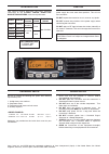
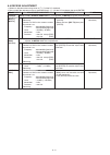
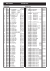
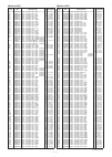
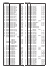
Summary of IC-F6021
Page 1
S-14601xz-c1 may. 2009 uhf mobile transceivers.
Page 2
This service manual describes the latest technical information for the ic-f6021, f6023/h, f6028h uhf mobile transceivers at the time of publication. Never connect the transceiver to an ac outlet or to a dc power supply that uses more than specified. This will ruin the transceiver. Do not expose the ...
Page 3
Table of contents section 1 specifications section 2 inside views section 3 disassembly instruction section 4 optional unit installation section 5 circuit descripiton 5-1 receiver circuits. . . . . . . . . . . . . . . . . . . . . . . . . . . . . . . . . . . . . . . . . . . . . . . . . . . . . . . . ...
Page 4: Section 1. Specifications
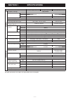
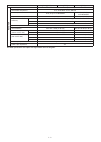
1 - 1 section 1. Specifications [usa], [chn] [exp] [eur] general • frequency coverage 400–470 mhz • type of emission wide 16k0f3e (25.0 khz) middle – 14k0f3e (20.0 khz) narrow 11k0f3e (12.5 khz) 8k50f3e (12.5 khz) • number of programable channels 128 channels (8 zones) • antenna impedance 50 Ω (nomi...
Page 5
1 - 2 all stated specifications are subject to change without notice or obligation. Measurements made in accordance with tia-603 or en 300 086. [usa], [chn] [exp] [eur] receiver • receive system double-conversion superheterodyne • intermediate frequencies 1st if; 46.35 mhz, 2nd if; 450 khz • sensiti...
Page 6: Section 2. Inside
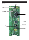
2 - 1 section 2. Inside views • front unit cpu (ic1) lcd driver (ic6) tone lpf (ic5) tone filter switch (q3) eeprom (ic3) clock frequency shift diode (d6) backlight controller (q5) dimmer controller (q2) backlight driver (q1) reset ic (ic2).
Page 7
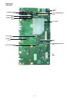
2 - 2 pll circuit • main-a unit (top view) if ic (ic1) lpf (q39) cpu5 line regulator (ic10) af amp (ic8) power switch (q23) +8 line regulator (ic9) discriminator switch (q5) power switch (q24) apc amp (ic2) 2nd if filter switch (q40) 1st if filter (fi1).
Page 8
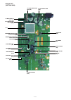
2 - 3 vco • main-a unit (bottom view) af/tone filters (ic16) af mute switch (q35, q36) ext. Modulation line switch (q31) reference frequency oscillator (x2) reference oscillator modulation amp (ic19) discriminator (x1) d/a converter (ic18) af pre-amp (ic15) expander (ic17) analog switch (ic14) d/a c...
Page 9: Section 3. Disassembly
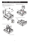
3 - 1 section 3. Disassembly instruction flat cable top cover front panel speaker cable main unit unsolder solder remover main unit main unit 1) unscrew 4 screws from the top cover, and remove the top cover. 2) disconnect the fl at cable and speaker cable. 3) unscrew 2 screws from the both sides, an...
Page 10: Section 4
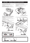
4 - 1 section 4 optional products installation install optional ut-108r as follows; 1) turn the transceiver power off, then disconnect the dc power cable. 2) unscrew 4 screws, then remove the bottom cover. 3) install the unit as shown below. 4) recover the bottom cover, screws and dc power cable. In...
Page 11: Section 5. Circuit
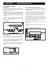
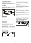
5 - 1 1st if circuits the rx signals from the bpf are mixed with the 1st lo signals to be converted into the 46.35 mhz 1st if signal. The 1st lo signals are generated by the rx vco (q14, d33, 62, 63), and passed through the lo sw (d15) and attenuator, then applied to the 1st mixer (q3) the converted...
Page 12
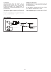
5 - 2 • rx af circuits af circuits the demodulated af signals from the if ic (ic1) are amplified and filtered by the hpf (ic16), and passed through the af line sw (ic14) and lpf (ic16). The filtered af signals are adjusted its level (=loudness) by the d/a converter (ic18), and applied to the af amp ...
Page 13
• tx af circuits • modulation circuits • tx amplifiers apc circuit 5 - 3 5-2 transmitter circuits mic amplifier (front unit) audio signals from the connected microphone are applied to the mic amp (ic5) via the microphone connector (j1). The amplifi ed mic signals are applied to the main unit. Tx af ...
Page 14
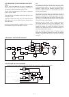
5 - 4 5-3 frequency synthsizer circuits vcos the tx vco which generates tx signal is composed by q13, d16, 64 and 65, and the frequency modulation is carried out by applying modulation signals to d18. The rx vco which generates 1st lo signals is composed by q14, d33, 62 and 63. These two vcos are sw...
Page 15
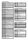
5 - 5 5-5-1 cpu (front unit; ic1) pin no. Port name description 1−3 kr1− kr3 input ports for dealer-programmable keys. 4−8 ks0− ks4 output ports for dealer-programmable keys. 10 ccs outputs chip-select signal to the attached optional unit. 19− 21 cenc0− cenc2 output ports for ctcss/dtcs signal. 23 d...
Page 16: Section 6. Adjustment
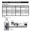
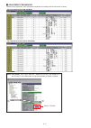
6 - 1 section 6. Adjustment procedure equipment grade and range equipment grade and range cloning software cs-f5020 : revision 1.0 or later jig cable modifi ed opc-1122u (see the illust below) dc power supply output voltage current capacity : 13.6 v dc except [eur] 13.2 v dc [eur] : 15 a except [eur...
Page 17
6 - 2 m adjustment frequencies before starting adjustment, clone adjustment frequencies and settings into the transceiver as below. • for [low band] version (400–470 mhz) • for [high band] version (450–512/520 mhz) select “middle” note: for [f6022], when adjust “deviation,” “modulation balance,” “rx...
Page 18
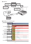
6 - 3 m adjustment utility window (example) m connection modulation analyzer (dc measurable) attenuator 40 db or 50 db to the antenna connector to dc cable standard signal generator –90 to +90 dbµ (–127 to –17 dbm) caution: do not transmit while ssg is connected to the antenna connector. Rf power me...
Page 19
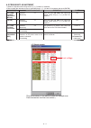
6 - 4 6-2 frequency adjustment 1) select an adjustment item using cursor or [ ↑ ] / [ ↓ ] of the pc’s keyboard. 2) set or modify the adjustment value as specifi ed using [ ← ] / [ → ] of the pc’s keyboard, then push [enter]. Adjustment adjustment condition operation value pll lock voltage -adjustmen...
Page 20
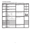
6 - 5 6-3 transmit adjustment 1) select an adjustment item using cursor or [ ↑ ] / [ ↓ ] of the pc’s keyboard. 2) set or modify the adjustment value as specifi ed using [ ← ] / [ → ] of the pc’s keyboard, then push [enter]. Adjustment adjustment condition operation value output power [power (hi)] 1 ...
Page 21
6 - 6 6-4 receive adjustment 1) select an adjustment item using cursor or [ ↑ ] / [ ↓ ] of the pc’s keyboard. 2) set or modify the adjustment value as specifi ed using [ ← ] / [ → ] of the pc’s keyboard, then push [enter]. Adjustment adjustment condition operation value receive sensitivity [bpf t1] ...
Page 22: Section 7
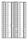
7 - 1 section 7 . Parts list m.=mounted side (t: mounted on the top side, b: mounted on the bottom side) [main-a unit] ref parts description m. H/v no. No. Location ic1 1110003491 s.Ic ta31136fng(d,el) t 57.8/24.7 ic2 1110002751 s.Ic ta75s01f(te85r,f) t 60/54.9 ic3 1150002380 ic ra30h4047m1-101 [eur...
Page 23
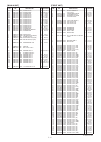
7 - 2 m.=mounted side (t: mounted on the top side, b: mounted on the bottom side) [main-a unit] ref parts description m. H/v no. No. Location r23 7030005050 s.Res erj2gej 103 x (10k) b 54.1/41.2 r29 7030005570 s.Res erj2gej 820 x (82) b 74/40.6 r30 7030005000 s.Res erj2gej 471 x (470) b 71.3/40.6 r3...
Page 24
7 - 3 m.=mounted side (t: mounted on the top side, b: mounted on the bottom side) [main-a unit] ref parts description m. H/v no. No. Location r308 7030009140 s.Res erj2gej 272 x (2.7k) t 56.9/54.9 r311 7030010040 s.Res erj2gej-jpw b 94.9/32.2 r313 7030005160 s.Res erj2gej 105 x (1m) t 31.4/6.8 r314 ...
Page 25
7 - 4 m.=mounted side (t: mounted on the top side, b: mounted on the bottom side) [main-a unit] ref parts description m. H/v no. No. Location c140 4030016930 s.Cer ecj0eb1a104k t 83.2/28.7 c141 4030017460 s.Cer ecj0eb1e102k t 77.9/22.2 c142 4030017460 s.Cer ecj0eb1e102k t 77.3/15.3 c143 4030017460 s...
Page 26
7 - 5 m.=mounted side (t: mounted on the top side, b: mounted on the bottom side) [main-a unit] ref parts description m. H/v no. No. Location c453 4030017420 s.Cer ecj0ec1h470j b 101.3/35.3 c454 4030017460 s.Cer ecj0eb1e102k b 100.4/35.3 c455 4030018860 s.Cer ecj0eb0j105k t 37.8/16.6 c457 4030017420...
Page 27
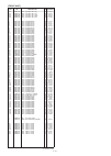
7 - 6 m.=mounted side (t: mounted on the top side, b: mounted on the bottom side) [front unit] ref parts description m. H/v no. No. Location r124 7030005120 s.Res erj2gej 102 x (1k) b 58.9/18.2 r125 7030005120 s.Res erj2gej 102 x (1k) b 58.9/19.1 r127 7030005160 s.Res erj2gej 105 x (1m) b 78/28.5 r1...
Page 28: Section 8. Mechanical
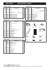
8 - 1 [chassis parts] ref order description qty. No. No. J1 6510004880 mr-dse-01 1 w1** 8900011800 opc-1199 1 mp1 8010019065 2601 chassis-5 [eur-01], [exp-01] 1 8010019135 2601 long chassis-5 [usa-01], [exp-03], [chn-01] 1 mp2 8110007821 2601 cover-1 1 mp3 8810008661 screw bt b0 3x8 ni-zc3 (bt) 8 mp...
Page 29
8 - 2 mp8 (c) x2 r14 (f) j1 (f) mp10 (f) mp12 (f) ep2 (f) w1 (f) mp3 (f) front unit unit abbreviations ( f): front unit (ma): main-a unit (c): chassis parts mp5 (f) mp9 (f) ds11 (f) mp2 (f) mp6 (f) mp1 (f) sp1 (f) mp11 (f) mp5 (c) x2 mp3 (ma) mp1 (c) j1 (c) mp4 (c) x2 main unit mp3 (c) x8 mp2 (c) mp...
Page 30: Section 9. Board
9 - 1 section 9. Board layouts • main-a unit (top view) • front unit (top view) sp+ 1 sp− 2 sp1 (front unit) antenna connector j1 (chassis) af out af gnd the combination of top side and bottom side of this page shows the actual configuration of p.C. Board. Unlk dim tone gnd sdec nois si ccs mic rssi...
Page 31: • Main-A Unit
9 - 2 • main-a unit (bottom view) • front unit (bottom view) the combination of top side and bottom side of this page shows the actual configuration of p.C. Board. Afo cpu5 pgio4 mic 8v batv ccs exst unlk plst si so tenc opv1 beep lvin tone rssi dast cdec temp sdec sck pgio3 m i d d n g pwon opt1 5v...
Page 32: Section 10
10 - 1 section 10 general wiring j1 1 2 3 4 5 6 7 8 j2 1 2 3 4 5 6 7 8 9 10 11 12 13 14 15 16 17 18 19 20 21 22 23 24 25 26 27 28 29 30 31 32 33 34 35 36 37 38 39 40 j2 1 2 3 4 5 6 7 8 9 10 11 12 13 14 15 16 17 18 19 20 21 22 23 24 25 26 27 28 29 30 31 32 33 34 35 36 37 38 39 40 j4 j7 1 2 w2 sp1 spe...
Page 33: Section 11. Block
11 - 1 section 11. Block diagram lpf lpf lpf lpf lpf ic16 njm12902 lpf ic16 njm12902 lpf q39 xp4601 lpf ic5 njm12902 lpf ic5 njm12902 pwr det d1:1ss375 d11:1ss375 ref x2 cr-794 mute sw q6:dtc144eu sw power q23:2sj506s q24:dtc144eu reset ic2 s-80942 ant sw d5:l709ce d6:1sv307 pwr amp ic3 ra30h4047m1 ...
Page 34: Section 12
*; refer to “parts list.” 12 - 1 section 12 section 12 . Voltage diagram c19 0. 1 ds5 sml-311yt c29 10 msva q3 d tc144eu c36 0. 1 ds4 sml-311yt c12 0.001 c27 270p ds7 sml-311yt c25 0.01 j1 1 2 3 4 5 6 7 8 l1 10u ds6 sml-311yt c9 0.001 c14 0.001 c26 0.1 ds9 sml-311yt c8 0.001 c28 0. 1 c16 0. 1 ds8 sm...
Page 35
12 - 2 *; refer to “parts list.” c main-a unit (1/2) r197 10k nw c 0.0068 c322 100k r378 0.01 c190 0. 1 c201 0. 1 c246 0 r381 47k r372 r314 100k 0. 1 c252 j7 1 2 3 4 r243 82k 0. 1 c264 0.001 c210 330k r377 r135 270k r252 100k r297 300k j6 1 2 3 4 5 6 7 8 9 10 11 12 13 14 15 hw-1-s w2 d42 dap222 tlva...
Page 36
12 - 3 *; refer to “parts list.” r1 100k r38 100k 0.001 c64 3p c308 r39 47 47p c63 r40 1.5k r36 3.9k 0.001 c348 0.001 c67 ta31136fng ic1 1 oscin 2 oscout 3 mixout 4 vcc 5 ifin 6 dec 7 filout 8 filin 9 afout 10 quad 11 ifout 12 rssi 13 n-det 14 n-rec 15 gnd 16 mixin 100p c61 r43 470 0.001 c66 r44 220...
Page 37
6f no.68, sec. 1 cheng-teh road, taipei, taiwan, r.O.C. Phone : +886 (02) 2559 1899 fax : +886 (02) 2559 1874 url : http://www.Asia-icom.Com e-mail : sales@asia-icom.Com zac de la plaine 1 rue brindejonc des moulinais bp 5804 31505 toulouse cedex, france phone : +33 (5) 61 36 03 03 fax : +33 (5) 61 ...
Page 38
1-1-32, kamiminami, hirano-ku, osaka 547-0003, japan s-14601xz-c1 © 2009 icom inc..

