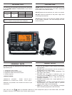
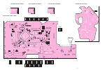
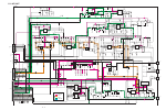
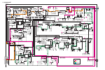
Summary of IC-M504
Page 1
Service manual vhf marine transceiver s-14225hz-c1- q dec. 2006.
Page 2
Introduction this service manual describes the latest service information for the ic-m504 marine transceiverat the time of publication. Ordering parts be sure to include the following four points when ordering replacement parts: 1. 10-digit icom parts number 2. Component name and informations 3. Equ...
Page 3
Table of contents section 1 specifications section 2 inside views section 3 disassembly instructions section 4 circuit descripiton 4-1 receiver circuits. . . . . . . . . . . . . . . . . . . . . . . . . . . . . . . . . . . . . . . . . . . . . . . . . . . . . . . . 4-1 4-2 transmitter circuits . . . ....
Page 4: Section 1
1 - 1 section 1 specifications m general • frequency coverage : tx rx 156.025–157.425 mhz 156.050–163.275 mhz ch70 rx 156.525 mhz • type of emission : 16k0g3e (fm), 16k0g2b (dsc) • antenna impedance : 50 Ω (nominal) • operating temperature range : –4˚f to +140˚f • power supply requirement : 13.8 v d...
Page 5
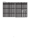
1 - 2 r e b m u n l e n n a h c a s u n a c t i m s n a r t e v i e c e r 1 0 0 5 0 . 6 5 1 0 5 6 . 0 6 1 a 1 0 0 5 0 . 6 5 1 0 5 0 . 6 5 1 2 0 0 0 1 . 6 5 1 0 0 7 . 0 6 1 3 0 0 5 1 . 6 5 1 0 5 7 . 0 6 1 a 3 0 0 5 1 . 6 5 1 0 5 1 . 6 5 1 0 0 2 . 6 5 1 0 0 8 . 0 6 1 a 4 0 0 0 2 . 6 5 1 0 0 2 . 6 5 1 ...
Page 6: Section 2
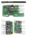
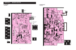
Section 2 inside views 2 - 1 dimmer control circuit q1: 2sb1201 q2, q3: ktc4075 system clock oscillator (x1: cr-790a) cpu (ic1: m30622mep-326gp) eeprom (ic3: hn58x2464ti) reset ic (ic4: s-80942cnmc-g9c) photo coupler (ic6: pc357n6j000f) 1st mixer [dsc channel] (d39: hsb88ws) fm if ic [normal-rx] (ic...
Page 7: Section 3
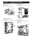
Section 3 disassembly instructions 3 - 1 • opening the transceiver case 1 unscrew 6 screws a. 2 disconnect 2 cables from j1 and j5. 3 remove the front unit. 4 unscrew 6 screws b, and remove the rear panel. Front unit j5 j1 rear panel a a a a a b b b b b b a b j4 j3 logic board j6 b b b a a b b c c a...
Page 8: Section 4
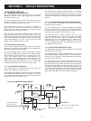
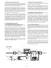
Section 4 circuit description 4-1 receiver circuit s 4-1-1 antenna switch (main unit) the received signals from the antenna connector are passed through the antenna switch which toggles the receive (rx) line and transmit (tx) line. The received signals from the antenna connector are passed through t...
Page 9
4-1-6 squelch circuits (main unit) noise squelch circuit mutes af output signals when no rf sig- nals are received. By detecting noise components (30 khz and higher signals) in the demodulated af signals, the squelch circuit switches the af mute switch on and off. A portion of the demodulated af sig...
Page 10
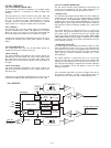
4-3 pll circuits 4-3-1 vco circuits (main unit) a vco (voltage controlled oscillator) is an oscillator whose oscillating frequency is controlled by adding voltage (lock voltage). This transceiver has 2 vco’s; rx vco (q72, d51, d52) and tx/ch70-rx vco (q4, q5, d1, d3). The rx vco oscillates the 1st l...
Page 11
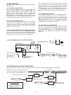
4-4 dsc cricuits the dsc circuits monitors the dsc channel ch70 (156.525 mhz) during stand-by. 4-4-1 rf circuits (main unit) the divided signals (dsc channel) are from the divider (l35, c151, c152) are applied to the rf amplifier (q61). The amplified received signals are passed through the bpf (l62,...
Page 12
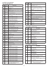
4 - 5 4-6 port allocations 4-6-1 cpu (logic unit; ic1) pin no. Port name description 1 dsenc outputs dsc encode signal to the lpf (af unit; ic8, pin 3). 2 beep outputs beep sounds to the af power amplifi er (ic9, pin 1). 3 pstb outputs pll strobe signal to the pll ic (main unit; ic1, pin 3). 4 extst...
Page 13: Section 5
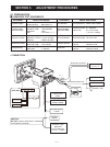
5 - 1 section 5 adjustment procedures ¤ required test equipments equipment grade and range equipment grade and range dc power supply output voltage : 13.8 v dc current capacity : more than 7 a dc voltmeter input impedance : 50 k Ω /v dc or better rf power meter (terminated type) measuring range : 0....
Page 14
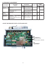
5 - 2 adjustment adjustment condition measurement value adjustment point unit location unit adjust lock voltage (regular receive) 1 • channel : ch16 (156.800 mhz) • receiving main connect a digital multi- meter or oscilloscope to the check point "cp2". 1.3–2.3 v main verify 2 • channel : ch16 (156.8...
Page 15
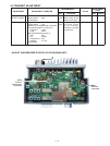
Adjustment adjustment condition measurement value adjustment point unit location unit adjust transmit output power 1 • channel : ch16 (156.800 mhz) • output power : high • transmitting rear panel c o n n e c t a n r f power meter to the antenna connector. 23–23.5 w main r112 deviation 1 • channel : ...
Page 16
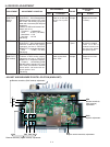
5 - 4 adjustment adjustment condition measurement value adjustment point unit location unit adjust receive sensitivity (regular receive) 1 • channel : ch16 (156.800 mhz) • [squelch] : max. Counterclockwise • set the internal speaker off in the set mode, and connect a distortion meter with a 4 Ω load...
Page 17: Section 6
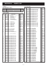
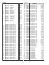
6 - 1 section 6 parts list m.=mounted side (t: mounted on the top side, b: mounted on the bottom side) [logic board] ref order description m. H/v no. No. Location ic2 1110006380 s.Ic lm2904pwr b 72.9/41.6 ic3 1140008650 s.Ic hn58x2464ti b 120.3/30.8 ic4 1110005771 s.Ic s-80942cnmc-g9ct2g b 134.9/61....
Page 18
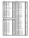
6 - 2 m.=mounted side (t: mounted on the top side, b: mounted on the bottom side) s.=surface mount [logic board] ref order description m. H/v no. No. Location c338 4030017460 s.Cer ecj0eb1e102k b 130.8/16.1 c339 4030017460 s.Cer ecj0eb1e102k b 145/16.4 c340 4030017760 s.Cer ecj0eb1h222k b 112.5/14.4...
Page 19
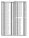
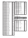
6 - 3 m.=mounted side (t: mounted on the top side, b: mounted on the bottom side) s.=surface mount [main unit] ref order description m. H/v no. No. Location r24 7030003410 s.Res erj3geyj 561 v (560) t 84.1/42.7 r25 7030003420 s.Res erj3geyj 681 v (680) t 85.4/43.2 r26 7030003620 s.Res erj3geyj 333 v...
Page 20
6 - 4 m.=mounted side (t: mounted on the top side, b: mounted on the bottom side) s.=surface mount [main unit] ref order description m. H/v no. No. Location c91 4030017620 s.Cer ecj0ec1h100c t 78/56.7 c92 4030017620 s.Cer ecj0ec1h100c t 78/58.6 c100 4550007520 s.Tan f931a106maabma t 65.6/49.2 c105 4...
Page 21
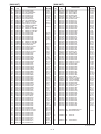
6 - 5 m.=mounted side (t: mounted on the top side, b: mounted on the bottom side) s.=surface mount [af unit] ref order description m. H/v no. No. Location ic3 1130011770 s.Ic cd4066bpwr t 35.5/25.5 ic4 1130011770 s.Ic cd4066bpwr t 78.5/24 ic5 1130011770 s.Ic cd4066bpwr t 59/47 ic6 1130011770 s.Ic cd...
Page 22
6 - 6 m.=mounted side (t: mounted on the top side, b: mounted on the bottom side) s.=surface mount [af unit] ref order description m. H/v no. No. Location c251 4030016790 s.Cer ecj0eb1c103k t 55.7/50 c260 4030017490 s.Cer c1608 jb 1a 105k-t t 82/27.8 c262 4030017460 s.Cer ecj0eb1e102k t 66.3/53.4 c2...
Page 23: Section 7
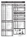
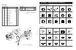
Section 7 mechanical parts and disassembly screw abbreviations a, b0, bt: self-tapping ph: pan head zk: black ni-zu: nickel-zinc sus: stainless mp1 mp5 mp2 mp3 mp4 ep1 mp11 w1 mp8 mp7 [chassis parts] j1 6510004880 connector mr-ds-e 01 1 w1 8900015070 cable opc-1546 1 w2 8900015080 cable opc-1547 1 w...
Page 24
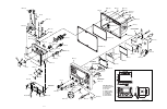
Unit: mm (inch) h g f a b c d e a d e b h i g f i c n m l j k j k l m n mp34 (c) w1 (a) mp32 (c) mp31 (c) mp33 (c) mp19 (c) mp18 (c) mp17 (c) w3 (c) w3 (c) w2 (c) w1 (c) mp44 (c) mp46 (c) mp13 (c) j1 (c) mp45 (c) mp12 (c) mp11 (c) mp7 (m) j1 (m) mp16 (c) mp15 (c) w2 (a) mp21 (c) mp22 (f) r1 (s) r1 (...
Page 25: Section 8
Section 8 semiconductor information • transistors and fet's b e c b c e b c e b b e e c c b e c b e c b e c b1 e b2 c1 c2 d s g2 g1 s d g b e c e1 e2 b2 c1 b1 c2 d d g d d s d g s b e c 2sa1576a t106 r 2sb1143 s 2sb1201 s 2sc4081 t106 s 2sc4226 t1 r25 2sk1069 4 tl 3sk292 fmw1 t148 kra304 (symbol: pd...
Page 26: Section 9
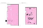
H5 h10 h15 h20 h25 h30 h35 h40 h45 h50 h55 h60 h65 h70 h75 h80 h85 h90 h95 h100 h0 v5 v10 v15 v0 v25 v30 v35 v20 v45 v50 v55 v40 v65 v60 1 2 to chassis unit w3 j5 vcc gnd rcv 20 19 2 1 to main unit j2 j2 att bpfv gnd nc mod detm sql unlk pck send h/l tmute txdet gnd gnd det70 s5v pstb pdata sp+ 1 2 ...
Page 27
H5 h10 h15 h20 h25 h30 h35 h40 h45 h50 h55 h60 h65 h70 h75 h80 h85 h90 h95 h100 h105 h110 h115 h120 h125 h0 v5 v10 v15 v0 v25 v30 v35 v20 v45 v50 v55 v40 v65 v60 hv 1 4 to af unit cp11-cp14 j1 hv gnd gnd 9 - 2 • bottom view (main unit) h5 h10 h15 h20 h25 h30 h35 h40 h45 h50 h55 h60 h65 h70 h75 h80 h...
Page 28
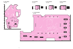
H5 h10 h15 h20 h25 h30 h35 h40 h45 h0 v5 v10 v15 v0 v25 v30 v35 v20 v45 v50 v55 v40 v65 v70 v60 hi/lo 9-3 hm-126 b/g • top view 9 - 3 h5 h10 h0 v5 v10 v0 volg 3 1 to logic board j3 w1 vol2 vol1 vo l 9-4 vr board • top view h5 h10 h0 v5 v10 v0 gnd 3 1 to logic board j3 w1 sqlv s5v sql 9-5 sql board •...
Page 29
H5 h10 h0 v5 v10 v15 v0 • bottom view (dial board) 9 - 4 h5 h10 h0 v5 v10 v0 • bottom view (sql board) h5 h10 h0 v5 v10 v0 • bottom view (vr board) h5 h10 h15 h20 h25 h30 h35 h40 h45 h0 v5 v10 v15 v0 v25 v30 v35 v20 v45 v50 v55 v40 v65 v70 v60 ptt • bottom view (hm-126 b/g ) h5 h10 h15 h20 h25 h30 h...
Page 30: Section 10
Section 10 block diagram 10 - 1 rx tx common voltage line data buff af amp af mute rx vco sp1 if amp r1 af mute tx/ ch70-rx vco af mute s1 c 1 1 2 2 3 4 4 8 5 buff ygr amp af mute x2:jtb450c24 450khz pwr amp af mute r1 x4:jtb450c24 450khz af mute af mute noise amp noise det apc ctrl af mute bpf cera...
Page 31: Section 11
Voltage line explanatory notes tx line rx line common line 100k r101 0.027 c44 100 r46 12 r86 1k r84 1k r95 0.001 c90 0.068 c81 4.7k r87 10 c102 47 r92 0.01 c108 0.001 c89 d1 kds122 0.001 c101 4.7k r94 10 c109 0.001 c88 0.01 c82 100k r85 ma8062 d4 4.7k r91 2sk1069 q9 22p c46 2sc4081 q5 820 r93 1k r9...
Page 32
Voltage line explanatory notes tx line rx line common line njm4558m ic7 1 2 3 4 5 6 7 8 820k r292 0.47 c311 njm4558m ic8 1 2 3 4 5 6 7 8 10k r293 la4485 ic14 1 ch1in 2 ch2in 3 s-gnd 4 btlin 5 btlout 6 fil ter 7 b-vcc 8 s-vcc 9 stby 10 mute 11 ch2out 12 b-gnd 13 ch1out m62429fp ic13 1 vin1 2 vout1 3 ...
Page 33
Voltage line explanatory notes tx line rx line common line 100k r203 1.0 µ l67 68 r624 3.3k r201 100k r172 0.1 c502 0.001 c136 1k r81 8.2k r42 0.01 c561 100k r386 0.001 c123 33p c185 1.5p c45 80n l4 ma77 d22 8p c181 0.01 c119 50n l71 470p c31 27p c625 q61 3sk292 0.001 c622 33k r26 1k r21 470p c380 0...
Page 34
& 0hone &ax 52, % mail :ac 0hone &ax 52, % mail 5nit 0hone &ax 52, % mail #tra 0hone &ax 52, % mail #orporate 0hone &ax 52, % mail #ustomer 0hone 'lenwood (ighway 0hone &ax 52, % mail 5nit 0hone &ax 52, % mail ! !Uckland 0hone &ax 52, % mail 2oom 9ong 0hone 52, % mail 3opot 0hone &ax % mail 0hone &a...
Page 35
1-1-32, kamiminami, hirano-ku, osaka 547-0003, japan s-14225hz-c1 - q © 2006 icom inc..

