- DL manuals
- Icom
- Receiver
- IC-R5
- Service Manual
Icom IC-R5 Service Manual
Summary of IC-R5
Page 1
Service manual communications receiver 1-1-32, kamiminami, hirano-ku, osaka, 547-0003, japan s-13905iz-c1 © 2002 icom inc..
Page 2
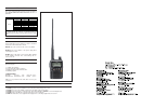
Introduction danger ordering parts repair notes this service manual describes the latest service information for the ic-r5 communications receiver at the time of publication. Never connect the receiver to an ac outlet or to a dc power supply that uses more than 6.5 v. Such a connection could cause a...
Page 3
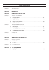
Section 1 specifications section 2 inside views section 3 disassembly instructions section 4 circuit descripiton 4-1 receiver circuits . . . . . . . . . . . . . . . . . . . . . . . . . . . . . . . . . . . . . . . . . . . . . . . . . . . . .4-1 4-2 pll circuits . . . . . . . . . . . . . . . . . . . ....
Page 4
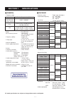
1 - 1 section 1 specifications m general • frequency range : • mode : fm, wfm, am • no. Of memory channel : 1250 channel (incl. Scan edge and auto memory right ch.) • frequency stability : ±6 ppm max. (–10˚c to +60˚) • tuning steps : 5, 6.25, 10, 12.5, 15, 20, 25, 30, 50, and 100 khz • anntena imped...
Page 5
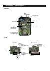
Section 2 inside views • logic unit 2 - 1 • rf unit af power amplifier (ic450: ta31056f) af mute switch (q350: 2sj144) eerom (ic2: cat24wc256) af filter (q301: xp6501) +3.2 regurater (ic103: r1111n321b) dc-dc convertor ic102: xc6371a351pr d105: rb551v battery charger circuit d503: ma133 d500: sb07-0...
Page 6
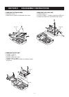
Section 3 disassembly instructions 3 - 1 • removing the rear panel 1 unscrew 2 screws, a . 2 remove the rear panel in the direction of the arrow. • removing the rf unit 1 unscrew 1 screw, b . 2 unsolder 4 points, c . 3 remove 1 knob, and 1 cap g . Unscrew 2 nuts, e and f . 4 unplug, h , to separate ...
Page 7
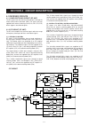
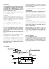
Section 4 circuit description 4 - 1 4-1 receiver circuits 4-1-1 band switching circuit (rf unit) the rf signals from the antenna connector pass through the limitter (d68) and an attenuator (d69). The signals are then applied to the antenna switching circuit (d13, d31, d73, d75) which suppress out-of...
Page 8
4 - 2 (3) 30–117.995 mhz, 175–329.995 mhz the 30 mhz–117.95 mhz, 175 mhz–329.995 mhz signals pass through the band switching circuit and low-pass filter (c40–c43, c665, c666, l9, l10, l92), and are then applied to the rf amplifier (q36). The amplified signals are amplified at the rf amplifier (ic11,...
Page 9
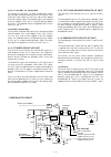
4 - 3 (2) wfm mode the 3rd if signal from the 3rd mixer bypasses the ceramic fil- ter (fi2) and fed back to the limiter amplifier section (pin 5). The amplified signal is demodulated at the quadrature detec- tor section (pins 10, 11) and detector coil (l21). The af sig- nals are output from pin 9 an...
Page 10
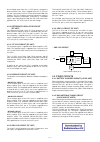
4 - 4 an oscillated signal from the 1st vco passes through the buffer amplifiers (ic4, q43) is applied to the pll ic (ic3, pin 19) and is prescaled in the pll ic based on the divided ratio (n-data). The pll ic detects the out-of-step phase using the reference frequency and outputs it from pin 13. Th...
Page 11
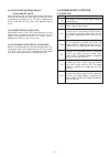
4 - 5 4-3-3 ear phone antenna circuit (logic and rf units) when switching to the ear phone antenna while wfm band receiving, the received rf signal passes through the exter- nal speaker jack (logic unit; j2). The signal is applied to the d101’s anode side (rf unit), and is then applied to the rf cir...
Page 12
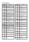
4 - 6 4-5 port allocations 4-5-1 cpu (logic unit; ic1) pin port description number name pin port description number name 2 3 4 5 6 7 14 15 19 25 26 28 30 31 32 33 34 43 44 45 46 47 k2 k1 rssi vin ctone rtone esio eck reset power hvdet cls clin clout pdaul pstb pck uhfc antsw wfm am noise input port ...
Page 13
4 - 7 pin port description number name 69 73 74 75 76 77 80–85 88–90, 92, 94–96 97 98 99–127 138 139 141 light dck dud sql func mode rxf1, rxf0, b3–b0 sec37–35, seg34, sec33–31 cont1 cont0 seg28–0 vrc fset trac outputs lcd back light control signal. High: lights on. Input port for the clock signal f...
Page 14
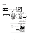
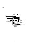
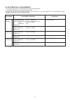
5 - 1 5-1 preparation some adjustments must be adjusted on the adjustment mode. When entering the adjustment mode, the 68 k Ω terminator is required. ‘ ‘ required test equipment ‘ ‘ entering the adjustment mode q connect a 68 k Ω terminator to the [sp] jack. W push and hold the [func] key, and then ...
Page 15
5 - 2 to the antenna connector standard signal generator 0.1 v to 32 mv ( 127 dbm to 17 dbm) optional sma bnc adaptor 1/8" (3.5 mm) 3-conductor plug 68 k + to [sp] jack power supply 6 v / 1 a jig ad-92sma power supply 3 v / 1 a power supply connection (ic-r5 has two pattern.) using [dc 6v] jack caut...
Page 16
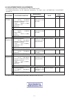
5 - 3 5-2 pll adjustment “reference frequency” adjustment must be performed at “adjustment mode”. 1st vco lock voltage 2nd vco lock voltage reference frequency detector output voltage adjustment adjustment adjustment condition measurement value point unit location unit adjust 1 2 3 4 5 1 2 1 1 • dis...
Page 17
5 - 4 l21 detector output voltage adjustment quad detector output voltage check point v 2nd vco lock voltage check point lv1 1st vco lock voltage check point f reference frequency check point l63 1st vco lock voltage adjustment bottom view • rf unit.
Page 18
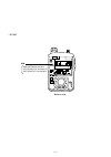
5 - 5 5-3 adjustment mode adjustments • the following adjustments must be performed at “adjustment mode”. • the following adjustments can be adjustned automatically. The detail shows “automatically adjustment” (at page 5-8). Bar antenna vhf sensitivity uhf sensitivity adjustment adjustment adjustmen...
Page 19
5 - 6 sen bar antenna check point vhf sensitivity check point uhf sensitivity check point • rf unit bottom view.
Page 20
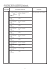
5 - 7 s-meter adjustment adjustment condition operation 1 2 3 4 5 6 7 8 9 10 11 12 • displayed frequency : (sm ch) 14.100 mhz • connect the ssg to the antenna connector and set as : level : 0.5 µv * (–113 dbm) modulation : off • mode : fm • receiving • set the ssg as :level : 1.6 µv * (–103 dbm) • m...
Page 21
5 - 8 5-4 automatically adjustments • the following adjustments must be performed at “adjustment mode”. • the following adjustments can be ajusted automatically. • in case of be finished to adjust “bar antenna”, “vhf sensitivity” and “uhf sensitivity” adjustments already, do not need to perform the ...
Page 22
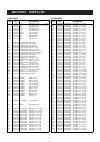
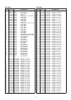
S.=surface mount ic1 1140010860 s.Ic m30220ma-121rp [usa] 1140010870 s.Ic m30220ma-120rp except [usa] ic2 1130011140 s.Ic cat24wc256k1.8 ic3 1110005820 s.Ic r3112n281a-tr ic100 1130007110 s.Ic tc7w04fu (te12l) ic102 1110004790 s.Ic xc6371a351pr ic103 1180002370 s.Reg r1111n321b-tr ic104 1180002370 s...
Page 23
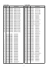
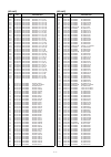
6 - 2 s.=surface mount r306 7030007340 s.Resistor erj2gej 153 x (15 k Ω ) r307 7030005050 s.Resistor erj2gej 103 x (10 k Ω ) r308 7030008290 s.Resistor erj2gej 183 x (18 k Ω ) r309 7030008290 s.Resistor erj2gej 183 x (18 k Ω ) r310 7030005310 s.Resistor erj2gej 124 x (120 k Ω ) r311 7030005240 s.Res...
Page 24
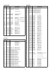
S.=surface mount j2 6450002010 s.Connector hsj1501-011010 j3 6510020560 s.Connector axk5s40340p j500 6450002130 connector 04-730a1-02bka ds1 5030001990 lcd ttr5169 upfdhw s6 2250000390 encoder tp90n00e20-16f-1995 s9 2230001070 s.Switch jpm1990-2711r s10 2230001070 s.Switch jpm1990-2711r w2 703001004...
Page 25
6 - 4 s.=surface mount l14 6200006990 s.Coil eljre 56ng-f l15 6200005740 s.Coil eljre 47ng-f l17 6200007170 s.Coil mlf1608a 3r3k-t l20 6200005740 s.Coil eljre 47ng-f l21 6150004840 s.Coil ls-510 l28 6200008090 s.Coil lqw2bhn68nj01l (lqn21a 68nj04) l39 6200005730 s.Coil eljre 39ng-f l40 6200005650 s....
Page 26
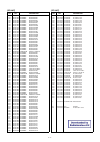
S.=surface mount r216 7030007290 s.Resistor erj2gej 222 x (2.2 k Ω ) r220 7030005300 s.Resistor erj2gej 150 x (15 Ω ) r221 7030007280 s.Resistor erj2gej 331 x (330 Ω ) r222 7030007290 s.Resistor erj2gej 222 x (2.2 k Ω ) r223 7030007290 s.Resistor erj2gej 222 x (2.2 k Ω ) r224 7030007300 s.Resistor e...
Page 27
6 - 6 s.=surface mount c176 4030017420 s.Ceramic ecj0ec1h470j c178 4030017460 s.Ceramic ecj0eb1e102k c180 4030017460 s.Ceramic ecj0eb1e102k c182 4030017460 s.Ceramic ecj0eb1e102k c183 4030017550 s.Ceramic ecj0ec1h1r5b c186 4030017460 s.Ceramic ecj0eb1e102k c188 4030017460 s.Ceramic ecj0eb1e102k c190...
Page 28
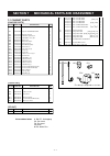
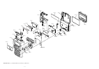
Section 7 mechanical parts and disassembly 7 - 1 screw abbreviations a, b0, bt: self-tapping ph: pan head fh: flat head zk: black ni-zu: nickel-zinc ref. No. Order no. Description qty. J1 6510020951 connector sma-r226-1 1 sp1 2510000960 speaker k036na500-26a27 1 mp1 8210019070 2605 front panel 1 mp2...
Page 29
7 - 2 unit abbreviation (c): chassis parts, (r): rf unit, (l): logic unit mp9 (c) 5 sp1 (c) mp4 (c) mp7 (c) mp11 (c) mp1 (c) mp14 (c) mp10 (c) mp6 (c) mp13 (c) mp23 (c) mp15 (c) mp2 (c) mp3 (c) mp26 (c) mp5 (c) mp22 (c) mp22 (c) mp19 (c) mp18 (c) mp17 (c) mp24 (c) mp24 (c) mp4 (l) mp8 (c) j1(c) rf u...
Page 30
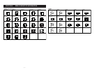
Section 8 semi-conductor information 8 - 1 b e c e c b e c b e c b e c b e c b e c b e c b e2 b2 b1 c2 e1 c1 b c e s d g s d g b e c b e c b e c e1 c2 b1 c1 e2 b2 b1 e b2 c1 c2 e1 c2 b1 c1 e2 b2 e1 c2 b1 c1 e2 b2 e1 e2 b2 c1 b1 c2 e1 b1 b2 c1 c2 s s s g d d d d 2sa1588 gr (symbol: zg) 2sc4617 s (sym...
Page 31
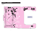
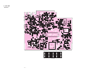
Section 9 board layouts 9 - 1 c133 c134 ic104 ic3 b5887d c136 c504 r108 r107 r109 r19 r 106 r57 r44 r450 c23 r25 c51 w7 w5 w4 w3 w2 w17 r17 c9 c7 c6 c12 c13 q5 q452 ep9 ep2 ep1 ic1 mp3 ds1 ep4 ep3 x1 c454 r24 r103 c29 c21 r27 r58 r451 r105 r59 c53 r64 r65 c116 r104 c45 c505 c25 c31 r28 r29 r30 r34 r...
Page 32
9 - 2 • bottom view c47 w13 w10 c26 w12 w11 w14 c500 c132 c503 c501 d500 d502 d501 l100 ic102 mp1 mp5 mp2 ic400 ic103 ic200 q200 ic100 c128 c305 q301 q300 c118 c453 c450 c458 c457 c452 d1 q2 ic2 ep11 j500 s6 c451 c401 c130 c129 c114 c115 q100 c113 c101 d503 r502 r501 r49 r45 r47 r43 r324 c317 c2 c30...
Page 33
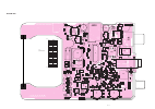
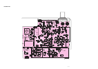
9 - 2 rf unit • top view c543 r236 r234 d69 l11 c47 l13 c50 c5 q26 c51 r110 r19 c45 r99 d13 d3 r233 r237 c546 c540 c19 c20 c218 r239 c23 c22 c21 l2 l5 l4 l39 l83 c517 c519 c518 c516 c567 r243 d63 r222 r225 r226 l86 c526 r223 c528 c171 d52 r128 r224 c199 c44 r106 l41 r108 l10 d31 c42 c570 c675 r98 c6...
Page 34
C264 c139 c554 c672 l40 c214 r93 r68 c138 c39 l1 d2 c234 c176 c103 c659 c259 r50 c203 c424 r121 c656 c81 c154 c80 r1 d17 c78 c79 c162 c211 r123 r188 d46 c182 c166 c158 c183 q30 d54 l63 r125 c178 c164 r67 c241 c434 c507 l77 fi1 c505 c233 c119 d25 d72 ic1 d1 l28 r79 r9 c13 c12 r8 c416 c10 l59 c512 c8 ...
Page 35
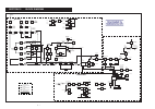
Section 10 block diagram 10 - 1 level conv bpf bpf bpf bpf bpf battery bpf bpf buff buff j500 04-730a1-02bka j1(chassis) sma-r226 matrix buff att lcd bpf lpf lpf d502 rb551v x1 cr-593 x1 cstcr6m75g53 lpf buff lpf bpf d18 hvu350b rf amp lim band sw ant sw band sw band sw bar ant fm if ic +3s fset shi...
Page 36
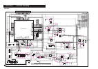
Section 11 voltage diagram • logic unit + + + + + + + + + + + + + + + ds1 ttr5169 1 com0 2 com1 3 com2 4 com3 5 seg37 6 seg36 7 seg35 8 seg34 9 seg33 10 seg32 11 seg31 12 seg28 13 seg27 14 seg26 15 seg25 16 seg24 17 seg23 18 seg22 19 seg21 20 seg20 21 seg19 22 seg18 23 seg17 24 seg16 25 seg15 26 seg...
Page 37
• rf unit 11 - 2 + + + + + + + c41 5 p r331 1 k r231 4.7 k r334 22 k c662 0.1 d34 1sv308 c48 6 p c145 470 p c37 c414 0.001 c54 0.001 d31 ma132wk r332 1 k q36 2sc5231 c8 c5 470 p c46 3 p l44 4.7 nh r110 12 k d71 1sv308 c47 6 p c148 470 p r6 120 l40 c42 3.5 p c35 10 p c671 0.001 c39 4 p d11 1sv308 d36...
Page 38: Service
Service manual communications receiver 1-1-32, kamiminami, hirano-ku, osaka, 547-0003, japan s-13905iz-c1 © 2002 icom inc..

