- DL manuals
- JCM
- Cash Register
- J3500E
- Service Manual
JCM J3500E Service Manual
Summary of J3500E
Page 1
1 electronic cash register j3500e service manual document no. 5190-02-03 rev.01 title : j3500e service manual draw check appr. Prepared by k. Sakaue 2004/12/6 approved by copy right 2004 by japan cash machine co., ltd..
Page 2
2 table of contents 1 introduction..................................................................................................................................................................1 2 installation procedure.................................................................................
Page 3
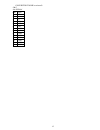
1 1 introduction j3500e consist of 5 block (1)main cpu board main cpu:m16c/80 renesas device 16 bit mpu ram 4m bit (battery back up) eprom 4m bit cmos (2) front display unit (3) rear display unit (4) key board unit (5) power supply unit 2 installation procedure 2.1 unpacking the ecr packing method i...
Page 4
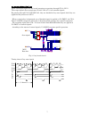
2 2.2 emergency cash drawer release in the unlikely event of a machine malfunction or a prolonged power failure, the model j3500e is equipped with an emergency cash drawer release. The release is located on the rear underside of the cash drawer. To manually release the drawer, carefully lift one sid...
Page 5
3 diagnostics (1) turn the mode lock key to “p” position, or assign to “p” mode(4---key). (2) enter xxxxxxxxx(9digit) --- #/ns 555555555-----#/ns automatic receipt issue at 3 minutes interval. 555555551-----#/ns automatic receipt issue at 5 second interval without cutter. 555555552-----#/ns automati...
Page 6
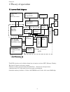
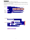
4 section 2 3 theory of operation 3.1 system block diagram scom3 is reserved the ecr circuitry can be broken down into six major sections: mpu, memory, display, key board, printer, and power supply. The heart of this system consists of a m16c/80, sixteen bit microprocessor implementing l.S.I, high s...
Page 7
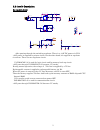
5 c46 104c 10 11 u12e sn74lv14apw_vbb + - bt1 3/v 280r r5 122 r43 103 1 tp2 test point 1 tp3 test point r42 103 c47 104c r44 103 10 11 u10e sn74lv14apw 12 13 u12f sn74lv14apw_vbb 1 2 3 4 cn2 b4p-vh d2 hzu15b2 vout 1 mnurst 2 vcc 3 gnd 4 u9 pst591cmt 12 13 u10f sn74lv14apw c3 104c r3 122 d3 hzu4.3b2 ...
Page 8
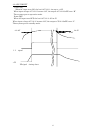
6 3.2.2 pf circuit power on when ac input turn on, the level of u12-11 rise up to +4.3v. When input voltage of u12-11 become 3.3v, the output of u12-12(npf) turn “h”. Then system goes to operation mode. Power off when ac input turn off, the level of u12-11 fall to 0v. When input voltage of u12-11 be...
Page 9
7 kr0 1 kr1 2 kr2 3 kr3 4 kr4 5 cn13 w-d0805#01 ks0 1 ks1 2 ks2 3 ks3 4 ks4 5 ks5 6 ks6 7 ks7 8 ks8 9 cn15 w-d0809#01 com 1 reg 2 x 3 z 4 p 5 sp 6 cn14 5267-06a ks[0..3] key scan key return control a 1 b 2 c 3 g1 6 g2a 4 g2b 5 y0 15 y1 14 y2 13 y3 12 y4 11 y5 10 y6 9 y7 7 u22 sn74lv138apwr a 1 b 2 c...
Page 10
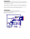
8 3.2.4. Display circuit display signals are applied to display circuit board via cn3. The display signals for digit indication are supplied from p120 to p127 and p145,p146 of cpu ports. The digit indication signals are amplified at 9 fets.(2sj208) and they are supplied to led common terminal on fd ...
Page 11
9 g d s q8 2sk2569 r cx rx/cx & 1 2 3 14 15 4 13 u16a sn74lv123apw s 2 d 6 d 7 s 3 g 4 s 1 d 5 d 8 q9 irf7424 d25 1ss226 r52 153 c69 104c r57 472 1 2 3 u5a sn74lv32apw - + 3 2 1 u19a lm393m r14 472 r60 103 r cx rx/cx & 9 10 11 6 7 12 5 u16b sn74lv123apw r58 222 c28 101c r53 473 9 10 8 u5c sn74lv32ap...
Page 12
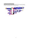
10 f2 ccp2e25 ph1 ph2 da0 +24v out1a 17 out2a 20 out1b 14 out2b 23 vcc 8 vbb 24 vref1 10 vref2 4 gnd 6 gnd 7 gnd 18 gnd 19 rc2 5 rc1 9 sense1 15 e1 16 sence2 22 e2 21 phase1 11 phase2 3 i01 13 i02 1 i11 12 i12 2 u18 udn2916lb 1b 3 1a 1 2b 4 2a 2 m cn8 b04b-pask-1 - + 3 2 1 u20a lmv358m r59 563 r55 5...
Page 13
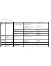
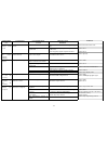
11 + 4 trouble shooting phenomenon condition considerable cause check point/method remedy ac power is not supplied ac power is not applied to switching power supply. Is ac power plug connected to outlet? Is outlet voltage normal? Is fuse (primary side of switching power supply? Is 24v output from se...
Page 14
12 phenomen on condition considerable cause check point/ method remedy is the head unit over heat? When the head is over heated, printing is stop. Wait for head becomes cool. Printer doesn’t work at all printer motor doesn’t rotate stepping signal does not generated. Is the stepping signal output fr...
Page 15
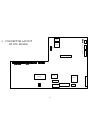
13 5 connector layout of cpu board cn 4 cn 5 cn 6 cn 17 cn16 cn15 cn13 cn14 c n 3 c n 11 c n 10 c n 9 c n 8 c n 7 p r o m r a m c p u c n 2 b a tt cn 1 c n 12 1 2 p r in t h ea d m o t o r sc o m 0 sc o m 1 sc o m 2 d isp la y p o w er dr w.
Page 16
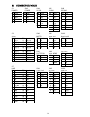
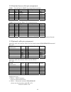
14 5.1 connector table cn1 cn2 cn4 cn5 cn6 drawer power scom0 scom1 scom2 pin signal pin signal pin signal pin signal pin signal 1 +24v 1 gnd 1 sg 1 sg 1 sg 2 drw 2 gnd 2 txd 2 txd 2 txd 3 drw sol 3 +24v 3 rxd 3 rxd 3 rxd 4 sg 4 +24v 4 rts 4 rts 4 rts 5 cts 5 cts 5 cts 6 vcc 6 dtr 6 dtr 7 dsr 7 dsr ...
Page 17
15 connector table (continued) cn17 3rd display pin signal 1 gnd 2 vcc 3 nc 4 l rs 5 l wr 6 l rd 7 l db0 8 l db1 9 l db2 10 l db3 11 l db4 12 l db5 13 l db6 14 l db7.
Page 18
16 5.2 standard inner cable pin assignment com1 5120-05-03 (for dos/v pin assign hand scanner) cn4 signal direction dsub 9pin(male) signal 1 sg gnd 5 sg 2 txd output 3 txd 3 rxd input 2 rxd 4 rts output 7 rts 5 cts input 8 cts 6 vcc power 9 vcc com2 5120-05-04 (for dos/ v pc communication) cn5 signa...
Page 19
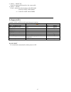
17 3. J3500-----dos/v pc it can be connected directly by the cross cable. 4. J3500-----gp965 case2 : please use the interface cable wi-1369. 5120-05-03+wi-1369 (com1) or 5120-05-04+wi-1369 (com2) 6 appendix number of plu & pb actually maximum occupation. Standard memory 256kb mem. Occ. Plu 12 char+p...
Page 20
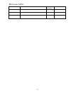
18 revision table date description rev. Number rom ver 2004/12/07 1 st edition .01 1.00-3.

