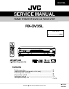
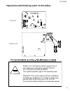
Service manual home theater dvd/cd receiver no.21124 jul. 2002 copyright 2002 victor company of japan, ltd. Rx-dv3sl rx-dv3sl contents safety precautions -------------------------------------------------------- importance administering point on the safety ---------------------- preventing static ele...
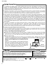
Rx-dv3sl 1-2 1. This design of this product contains special hardware and many circuits and components specially for safety purposes. For continued protection, no changes should be made to the original design unless authorized in writing by the manufacturer. Replacement parts must be identical to th...
Rx-dv3sl 1-3 caution: for continued protection against risk of fire, replace only with same type 5a/125v for f101, 2a/125v for f202 and f203. This symbol specifies type of fast operating fuse. Precaution: pour eviter risques de feux, remplacez le fusible de surete de f101 comme le meme type que 5a/1...
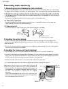
Rx-dv3sl 1-4 preventing static electricity 1. Grounding to prevent damage by static electricity electrostatic discharge (esd), which occurs when static electricity stored in the body, fabric, etc. Is discharged, can destroy the laser diode in the traverse unit (optical pickup). Take care to prevent ...
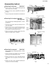
Rx-dv3sl 1-5 remove the four screws marked a attaching the top cover on both sides of the body. Remove the three screws marked b on the back of the body. Remove the top cover from behind in the direction of 1. 2. 3. Disassembly method removing the top cover (see fig.1) prior to performing the follow...
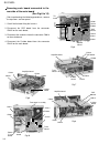
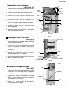
Rx-dv3sl 1-6 prior to performing the following procedures, remove the top cover and rear panel. Cut off the tie band fixing the harness. Disconnect the dsp board from the connector cn612 on the main board, disconnect the card wire frome the connecter cn614 on the main board. Disconnect the s-video b...
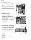
Rx-dv3sl 1-7 remove the six screws marked h attaching the heat sink. Unsolder the two p ower ics solder points attaching the rear side of the amplifier board. Pull out the amplifier board from the bracket hooks on the heat sink. 1. 2. 3. Removing the power ics (see fig.13, 14) prior to performing th...
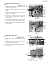
Rx-dv3sl 1-8 prior to performing the following procedures, remove the top cover, rear cover and dsp board. Remove the dvd / cd unit dust proof cover attaching on the main board. Remove the three screws marked i attaching the dvd /cd unit. Disconnect the connectors cn512 and cn513 on the main board. ...
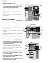
Rx-dv3sl 1-9 prior to performing the following procedure, remove the top cover and rear panel. Disconnect the harness connected to the connector cn101 on the power / fuse board (if necessary, cut off the band fixing the harness on the side of the base chassis). Unsolder the power cord and other harn...
Rx-dv3sl 1-10 prior to performing the following procedures, remove the top cover and front panel assembly. Remove the two screws marked q attaching the power switch board. Remove the seven screws marked r attaching the system control board. Remove the two screws marked s attaching the indicator boar...
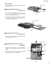
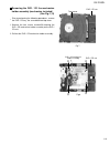
Rx-dv3sl 1-11 push the cam lever toward the center side of the dvd / cd unit in the direction of the arrow and draw the dvd / cd tray toward the front. Push the two tray stoppers marked a on the dvd / cd tray in the direction of the arrow and draw the dvd / cd tray toward the front. 1. 2. Prior to p...
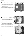
Rx-dv3sl 1-12 prior to performing the following procedures, remove the dvd / cd tray. Remove the four screws marked a attaching the top cover on the dvd / cd unit. Pull the top cover toward the direction of the arrow and draw the top cover toward the upper side. Removing the the top cover (see fig.4...
Rx-dv3sl 1-13 prior to performing the following procedures, remove the dvd / cd tray, the servo board and top cover. Remove the four screws marked d attaching the dvd / cd mechanism holder assembly on the dvd / cd unit. Pull out the dvd / cd mechanism holder assembly. 1. 2. Removing the dvd / cd the...
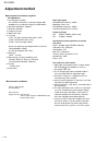
Rx-dv3sl 1-14 adjustment method measurement instruments required for adjustment 1. Low frequency oscillator, this oscillator should have a capacity to output 0dbs to 600ohm at an oscillation frequency of 50hz-20khz. 2. Attenuator impedance : 600ohm 3. Electronic voltmeter 4. Frequency counter 5. Wow...
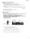
Rx-dv3sl 1-15 master volume dvd/super vcd/vcd/cd input att. Rec mode input analog/digital compact super video setting adjust memory r x - d v 3 h o m e t h e a t e r d v d / c d r e c e i v e r on/off surround mode fm/am tape/cdr source name tv vcr dbs dvd control standby standby/on + – + – 2 3 1 5 ...
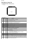
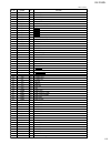
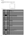
Rx-dv3sl 1-16 1 2 3 4 5 6 7 8 9 10 11 33 32 31 30 29 28 27 26 25 24 23 12 13 14 15 16 17 18 19 20 21 22 44 43 42 41 40 39 38 37 36 35 34 1. Pin layout ak4527bvqp (ic601) : a/d,d/a converter top view no. 1 2 3 4 5 6 7 8 9 10 11 12 13 14 15 16 17 18 symbol sdos osks mis bick lrck sdti1 sdti2 sdti3 sdt...
Rx-dv3sl 1-17 no. 19 20 21 22 23 24 25 26 27 28 29 30 31 32 33 34 35 36 37 38 39 40 41 42 43 44 symbol icks adif cad1 cad0 lout3 rout3 lout2 rout2 lout1 rout1 lin- lin+ rin- rin+ vrefl ovf vcom vrefh avdd avss xti xto p1s cs csn dif1 scl/cclk loop0 sad/cdti cdtd connect to gnd no internal bonding. A...
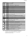
Rx-dv3sl 1-18 1. Pin layout mn101c35dkf (ic701) : panel micom 1 25 75 51 100 76 26 50 ~ ~ ~ ~ 1 2 3 4 5 6 7 8 9 10 11 12 13 14 15 16 17 18 19 20 21 22 23 24 25 26 27 28 29 30 31 32 33 34 35 36 37 38 39 40 41 42 43 pin no. Symbol txd/sbo0/p00 rxo/sbi0/p01 sbt0/p02 sbi1/p04 sbt1/p05 buzzer/p06 sbo1/p0...
Rx-dv3sl 1-19 44 45 46 47 48 49 50 51 52 53 54 55 56 57 58 59 60 61 62 63 64 65 66 67 68 69 70 71 72 73 74 75 76 77 78 79 80 81 82 83 84 85 86 87 pin no . Symbol i/o p52 p53 p54 dgt17/p67 88 89 90 function 91 92 93 94 95 96 97 98 99 seg42/pd0 100 vpp o o o o o o o o o o o o o o o o o o o o o o o o o...
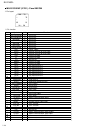
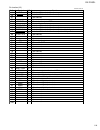
Rx-dv3sl 1-20 pin no. Symbol i/o function mn101c49gkg (ic761) : system micom 1 25 75 51 100 76 26 50 ~ ~ ~ ~ 1. Pin layout 2. Pin function 1 vref - connect to gnd 2 pa0 i ntstel(rgbesl) 3 pa1 i vcr s/c sw 4 pa2 i dbs s/c sw 5 pa3 i safety 6 pa4 i short&th det (a/d) 7 pa5 i outlevel detect (a/d) 8 pa...
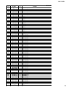
Rx-dv3sl 1-21 pin no. Symbol i/o function 44 sbt1 o dsp clk 45 cbo3 o vol data 46 sbi3 o vol latch 47 sbt3 o vol clk 48 mp3 o d.O.Mute 49 int/prog o int/prog 50 key0 o headphone relay 51 key1 o eedo 52 key2 o eedi 53 key3 o eeck 54 key4 o eecs 55 key5 o front spk relay 56 key6 o center spk relay 57 ...
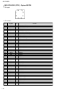
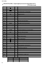
Rx-dv3sl 1-22 pin no. Symbol i/o function upd784215agc167 (ic681) : dital signal controller 1 25 75 51 100 76 26 50 ~ ~ ~ ~ 1. Pin layout 2. Pin function (1/2) vdd x2 x1 vss xt2 xt1 reset autodata lock digital0 format channel err rest in avdd avref0 avss av ref1 rx tx dspcom dspsts dspclk dsprdy mid...
Rx-dv3sl 1-23 upd784215agc167 pin no. Symbol i/o function 49 50 51 52 53 54~63 64 65 66 67 68 69 70 71 72 73 74 75 76 77 78 79 80 81 82 83 84 85 86 87 88 89 90 91 92 93 94 95 96 97 98 99 100 milp miack dsprst codec out codec in codec clk codec cs codec xts pd gnd vdd ana/t-tone lef-mix d.Mute s.Mute...
Rx-dv3sl 1-24 dlcks terminal l l h h dlonterminal l h l h dll clock setting scki input (dll circuit off) four times xi clock three times xi clock six times xi clock 1 2 3 4 5 6 7 8~11 12 13 14 15 16~18 19 20 21 22 23 24 25 26 27,28 29~30 31 32,33 34 35 36 37 38,39 40 41 42 43 44 45 46 47 48 49 50 51...
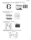
Rx-dv3sl 1-25 1 3 2 in b gnd in a 5 4 vcc out y tc7set32fu (ic683) : z-input or gate 1 1a 2 1b 3 1y 4 2a 5 2b 6 2y 7 14 13 12 11 10 9 8 gnd vcc 4b 4a 4y 3b 3a 3y tc74hcu08af (ic612) : inverter a l l h h b l h l h y l l l h 2.The truth value table 1. Pin layout / block diagram 1. Pin layout / block d...
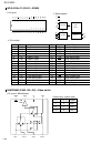
Rx-dv3sl 1-26 nc a16 a14 a12 a7 a6 a5 a4 a3 a2 a1 a0 i/o1 i/o2 i/o3 vss 1 2 3 4 5 6 7 8 9 10 11 12 13 14 15 16 32 31 30 29 28 27 26 25 24 23 22 21 20 19 18 17 v dd a15 cs2 we a13 a8 a9 a11 oe a10 cs1 i/o8 i/o7 i/o6 i/o5 i/o4 1. Pin layout w24l010aj-12 (ic641) : sram decoder core array control data i...
Rx-dv3sl 1-27.
200207 victor company of japan, limited audio & communication business division personal & mobile network business unit. 10-1,1chome,ohwatari-machi,maebashi-city,371-8543,japan (no.21124) rx-dv3sl.

