- DL manuals
- Lanner Electronics
- Firewall
- FW-7650 Series
- User Manual
Lanner Electronics FW-7650 Series User Manual
Summary of FW-7650 Series
Page 1
Fw-7650 series 19” 1u intel pentium4 / celeron rackmount network security platform user’s manual.
Page 2: Copyright and Disclaimers
Ii copyright and disclaimers © copyright 2004 - lanner electronics inc. All rights reserved the contents in this publication have been thoroughly checked and considered accurate. The publisher and manufacturer of this product, lanner electronics, is not responsible for any violation of patents or ot...
Page 3: Safety Instructions
Iii safety instructions the following information relates to the safety of installation and maintenance personnel. Read all instructions before attempting to unpack, install or operate this equipment, especially before connecting the power adapter. Please keep the following in mind as you unpack and...
Page 4: About This Manual
Iv getting technical assistance should you encounter questions or problems with your fw-7650, lanner electronics is ready to assist you within the guidelines of our product support programs. First, check the electronic product documentation for assistance. If you still cannot find the solution to yo...
Page 5: Table of Contents
V table of contents copyright and disclaimers....................................................................................................Ii trademark acknowledgments...............................................................................................Ii radio frequency emissions not...
Page 6
Vi 3.4 bios features setup .................................................................................. 27 3.5 chipset features setup............................................................................... 30 3.6 integrated peripherals ......................................................
Page 7: C H A P T E R 1
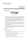
1 c h a p t e r 1 getting started 1.1 introduction figure 1 – fw-7650 outlook the fw-7650 is a 1u rackmount network security solution targeting the enterprise market. The fw-7650 supports petium4 /celeron processor with 400/533mhz fsb. It is designed with an intel 845gv as its northbridge and ich4(8...
Page 8: 1.2 Technical
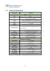
2 1.2 technical specifications model name fw-7650 sbc sbc mb-x71 cpu socket 478 for intel ® pentium ™ 4/celeron processor, up to 2.4ghz,533mhz fsb chipset intel ® 845gv chipset (pin-to-pin compatible with 845g series); 82801db i/o controller hub 4 (ich4) bios award bios memory two ddr200/266/333 dim...
Page 9: 1.3 Packing
3 1.3 packing contents carefully unpack your package and make sure that you have the following items. Fw-7650 network security platform console cable 1.8 meters long cross-over ethernet cable 1.8 meters long straight-through ethernet cable face panel name plate label power cable drivers and user’s m...
Page 10: 1.4 Mb-X71
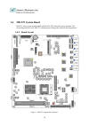
4 1.4 mb-x71 system board mb-x71 is the system board bundled with the fw-7650 network security platform. The succeeding sections list all mb-x71 related jumper settings and connector pin assignments. 1.4.1 board layout figure 3 – mb-x71 jumpers and connectors.
Page 11
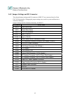
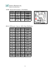
5 1.4.2 jumper settings and i/o connector the onboard jumper settings and i/o connector of mb-x71 are custom-tailored to fit the fw-7650 functionality. Changing the jumper settings may result in system malfunction or unforeseen damages. Jumper settings and i/o connector summary for mb-x71 jumper fun...
Page 12
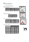
6 1.4.3 connector pin assignments sfc1:master/slave select compact flash card ata disk chip scf1 master slave 1-2 slave master 2-3(default cmos1:clear cmos data cmos1 description 1-2 normal (default) 2-3 clear cmos fan1~3 : 3 pin fan connector pin no. Description 1 ground 2 +12v 3 fan status lana1~2...
Page 13
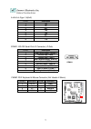
7 lana3~6 :type 1 ( rj-45) pin no. Description 1 tx+ 2 tx- 3 rx+ 4 t45 5 t45 6 rx- 7 t78 8 t78 coma1: rs-232 serial port #1 connector ( d-sub ) pin no. Description 1 data carrier detect ( dcda # ) 2 receive data ( rxda ) 3 transmit data ( txda ) 4 data terminal ready ( dtra # ) 5 ground ( gnd ) 6 da...
Page 14
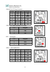
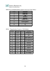
8 psa1:20 pin atx power connector pin no. Description pin no. Description 1 +3.3v 11 +3.3v 2 +3.3v 12 -12v 3 gnd 13 gnd 4 +5v 14 switch 5 gnd 15 gnd 6 +5v 16 gnd 7 gnd 17 gnd 8 power good 18 -5v 9 stand-by 5v 19 +5v 10 +12v 20 +5v ps4p1:4-pin power connector (p4-4p male ) pin no. Description 1 gnd 2...
Page 15
9 vgab1 : external vga connector ( 12 pin header ) pin no. Description pin no. Description 1 r 2 ground 3 g 4 ground 5 b 6 ground 7 h-sync 8 ground 9 v-sync 10 ground 11 detect-display data 12 deteck-display clock idea1 : ide interface connector ( 44pin 2.0mm pitch header ) pin no. Description pin n...
Page 16
10 plrs1:power led,hd led,reset,speaker connector(11 pin 2.54mm ) pin no. Description 1 power led + 2 power led + 3 gnd 4 hdd led + 5 hdd led - 6 reset sw + 7 reset sw – (gnd) 8 external speaker - 9 internal buzzer - 10 nc 11 external speaker + fdca1 : floppy interface connector ( 34 pin header ) pi...
Page 17
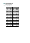
11 cf1:compact flash connector pin no. Description pin no. Description 1 gnd 26 cd1- 2 data3 27 data11 3 data4 28 data12 4 data5 29 data13 5 data6 30 data14 6 data7 31 data15 7 ce1# 32 ce2# 8 a10 33 vs1# 9 oe# 34 ior# 10 a9 35 iow# 11 a8 36 we# 12 a7 37 ready# 13 cfvcc3 38 cfvcc3 14 a6 39 csel 15 a5...
Page 18
12 lede1 : 2x22 pin pin no. Description pin no. Description 1 power led 2 power led 3 power led status 4 power led status 5 lan1 link/active led- 6 lan1 link/active led+ 7 lan1 100 led- 8 lan1 100 led+ 9 lan1 1g led- 10 lan1 1g led+ 11 lan2 link/active led- 12 lan2 link/active led+ 13 lan2 100 led- ...
Page 19
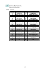
13 ideb1 : ide interface connector ( 40pin 2.54mm pitch header) pin no. Description pin no. Description 1 reset # 2 ground 3 data 7 4 data 8 5 data 6 6 data 9 7 data 5 8 data 10 9 data 4 10 data 11 11 data 3 12 data 12 13 data 2 14 data 13 15 data 1 16 data 14 17 data 0 18 data 15 19 ground 20 nc 21...
Page 20
14 pcib1:124 pin mini pci socket pin no. Description pin no. Description 1 tip 2 ring 3 8pmj-3 4 8pmj-1 5 8pmj-6 6 8pmj-2 7 8pmj-7 8 8pmj-4 9 8pmj-8 10 8pmj-5 11 led1_grnp 12 led2_yelp 13 led1_grnn 14 led2_yelp 15 chsgnd 16 reserved 17 int-b 18 +5v 19 +3.3v 20 int-a 21 reserved 22 reserved 23 ground...
Page 21
15 pcib1:124 pin mini pci socket (continued last page) pin no. Description pin no. Description 61 irdy 62 ground 63 +3.3v 64 frame 65 clkrun 66 trdy 67 serr 68 stop 69 ground 70 +3.3v 71 perr 72 devsel 73 c_be-1 74 ground 75 ad14 76 ad15 77 ground 78 ad13 79 ad12 80 ad11 81 ad10 82 ground 83 ground ...
Page 22: 1.5
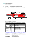
16 1.5 fw-7650 19” 1u rackmount firewall mechanisms this section of the manual describes the mechanical and device nomenclature of fw-7650. 1.5.1 face panel figure 5 – fw-7650 face panel face panel led status and behavior the following table lists and explains the behavior of each led on the fw-7650...
Page 23: 1.5.3 Rear View
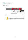
17 1.5.3 rear view figure 6 – fw-7650 rear view power switch: click the power switch , and the system will be power on. Faulty or improper use of the power adaptor may cause permanent damage to the power supply and the fw-7650. Plug the adaptor to an electrical wall outlet that matches its specifica...
Page 24: C H A P T E R 2
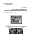
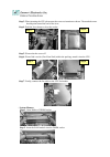
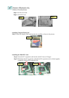
C h a p t e r 2 fw-7650 hardware installation guide 2.1 hardware installation guide inside of fw-7650 - cpu installation step 1 : locate the zif socket and open it by first pulling the lever of socket upward. Step 2 : insert the cpu into the socket. Please keep the lever right angle when inserting c...
Page 25
Step 3 : when inserting the cpu please note the correct orientation as shown. The notched corner should point toward the end of the lever step 4 : push the lever down to close the socket. Step 5 : please take the screw off. Step 6 : please find a cooler (fan+heat sink) within the packing, attach it ...
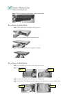
Page 26
Step 3 : press the latches into the notches of the ram module. How to remove the hard disk bay step 1 : open both latches of mobile rack by press it. Step 2 : use two hands to pull out the mobile rack. Step 3 : remove the mobile rack straight and smooth. How to remove the hard disk bay step 1 : use ...
Page 27
Step 5 : put the cover back. Step 6 : screw the cover. - installing compact flash card step 1 : insert the compact flash card into the slot carefully as shown in the picture. - installing the mini-pci card step 1: insert the pci expansion card into the mini-pci slot at 45 degree. Step 2: push down t...
Page 28: Chapter 3
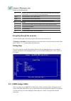
Chapter 3 award bios setup 3.1 bios setup award‘s rom bios provides a built-in setup program that allows users to modify the basic system configuration and settings. The modified data will be stored in a battery-backed cmos ram so that this data will be retained even when the power is turned off. In...
Page 29: Getting Help
Main menu - quit and not save changes into cmos status page setup menu and option page setup menu - exit current page and return to main menu increase the numeric value or make changes decrease the numeric value or make changes general help, only for status page setup menu and option page setup menu...
Page 30
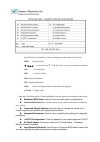
Listed below are explanation of the keys displayed at the bottom of the screen: : exit the utility. Ç È Æ Å > : use arrow keys Ç È Æ Å to move cursor to your desired selection. : general help : previous values : fail-safe defaults : optimized defaults : saves all changes made to setup and exits prog...
Page 31
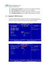
Set supervisor password: use this menu to set supervisor passwords set user password: use this menu to set user passwords. Save & exit setup: save cmos value changes to cmos and exit setup exit without saving: abandon all cmos value changes and exit setup 3.3 standard cmos features the items in stan...
Page 32
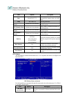
Item options description date month dd yyyy set the system date. Note that the ‘day’ automatically changes when you set the date time hh : mm : ss set the system time ide channel 0 master options are in its sub menu press to enter the sub menu of detailed options ide channel 0 slave options are in i...
Page 33: 3.4 Bios Features Setup
Ide channel 0 master none auto manual selecting ‘manual’ lets you set the remaining fields on this screen. Selects the type of fixed disk. "user type" will let you select the number of cylinders, heads, etc. Note: precomp=65535 means none ! Capacity auto display your disk drive size disk drive capac...
Page 34: Virus Warning:
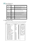
Virus warning: the default setting of virus warning is “disabled”. When it is enabled, any attempt to write the boot sector and partition table will halt the system and cause a warning message to appear. If this happens, you can use an anti-virus utility on a virus free, bootable floppy diskette to ...
Page 35: Video Bios Shadow :
Ps/2 mouse function control : when this option is set enabled , amibios supports a ps/2 type mouse. The settings are enabled or disabled . The default setting is disabled . System boot up sequence. Hdd s.M.A.R.T. For capability : this allows you to activate the s.M.A.R.T. (self-monitoring analysis &...
Page 36: Dram Clock :
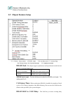
3.5 chipset features setup dram clock : the chipset support synchronous and asynchronous mode between the host clock and dimm clock. Host clk (default) dimm clock equal to host clock 66mhz dimm clock equal to 66mhz sdram cycle length : this item allows you to select the sdram cycle length. The setti...
Page 37: Dram Ras# Precharge Time:
Between the cas and ras strobe signals, used when dram is written to, read from, or refreshed. Fast gives faster performance. This field applies only when synchronous dram is installed in the system. Dram ras# precharge time: if an insufficient number of cycles is allowed for the ras to accumulate i...
Page 38: Ide Prefetch Mode :
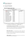
3.6 integrated peripherals on-chip (primary/secondary) pci ide : the intel 82c440bx chipset contains a pci ide interface with support for two ide channels. Select enabled to activate the primary and/or secondary ide interface. Select disabled to deactivate this interface, if you install a primary an...
Page 39: Usb Keyboard Support :
Usb keyboard support : select enabled if your system contains a universal serial bus (usb) controller and you have a usb keyboard. Init display first : this item allows you to decide to active whether pci slot of vga card or agp first. The settings are “pci slot” and “agp slot”. Onboard fdd controll...
Page 40
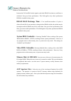
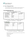
3.7 power management setup the power management setup allows you to configure you system to most effectively save energy while operating in a manner consistent with your own style of computer use. This category allows you to select the type (or degree) of power saving and is directly related to the ...
Page 41: Video Off Option :
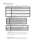
There are four selections for power management, three of which have fixed mode setting disable (default) no power management. Disables all four modes. Min. Power saving minimum power management. Doze mode=1hr. Standby mode =1hr., suspend mode=1hr., and hdd power down=15min. Max. Power saving maximum...
Page 42: 3.8 Pnp/pci Configuration
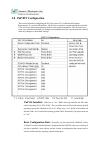
3.8 pnp/pci configuration this section describes configuring the pci bus system. Pci, or p ersonal c omputer i nterconnect, is a system which allows i/o devices to operate at speeds nearing the speed the cpu itself uses when communicating with its own special components. This section covers some ver...
Page 43: Resource Controlled By :
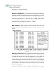
The settings are : “enabled and disabled”. Resource controlled by : the award plug and play bios has the capacity to automatically configure all of the boot and plug and play compatible devices. However, this capability means absolutely nothing unless you are using a plug and play operating system s...
Page 44: Dma Resources :
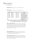
Isa/eisa and pci/pnp. Dma resources : the sub menu can let you control the dma resource. Dma resources : the sub menu can let you control the dma resource. Dma channel 0/1/3/5/6/7: these items specify the bus that the system dma(direct memory access) channel is used. The settings determine if amibio...
Page 45: Pci/vga Palette Snoop :
C0000,c4000,c8000,cc000,d0000,d4000,d8000,or dc000. Pci/vga palette snoop : leave this field at “disabled”. The settings are “enabled”, “disabled”. Pci latency timer (pci clocks): this option is used to control pci latency timer period (follow pci clocks). Based on pci specification 2.1 or later and...
Page 46: 3.9 Pc Health Status
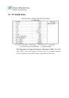
3.9 pc health status cpu temperature, fan1 speed, fan2 speed , fan2 speed, vcore, +2.5, +3.3v, +5v, +12v : these items display the current status of all monitored hardware devices/components such as system voltages, temperatures and fan speeds..
Page 47: 3.10 Load Optimized Defaults
3.10 load optimized defaults when you press “enter” on this item, you get a confirmation dialog box with a message similar to: load optimized defaults (y/n) ? N pessing “y” loads the default values that are factory settings for optimal performance system operations 3.11 supervisor/user password sett...
Page 48: 3.13 Exit Without Saving
3.13 exit without saving pressing on this item asks for confirmation: q u i t w i t h o u t s a v i n g ( y / n ) ? Y this allows you to exit setup without storing in cmos any change. The previous selections remain in effect. This exits the setup utility and restarts your computer..
Page 49: Power Supply
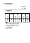
Appendix a power supply power supply specification ac input spec : voltage 100 - 240 vac full range (±10% tolerance) output specifications output voltage output current min. Output current max. Regulation load regulation line output ripple & noise max 5v 3 25.00 ± 5% ± 1% 50mv 12v 2 8.00 ± 7% ± 1% 1...
Page 50: Watchdog Timer
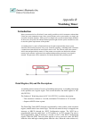
Appendix b watchdog timer introduction most systems need to be self-reliant. It's not usually possible to wait for someone to reboot them if there are some component wrong. Some system designs, such as space probes, are simply not accessible to human operators. If the system ever hangs, such systems...
Page 51
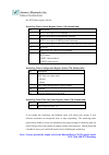
The wdt status register will set . Watch dog timer control register (index =71h, default=00h) bit description 7 wdt is reset upon a cir interrupt 6 wdt is reset upon a kbc(mouse) interrupt 5 wdt is reset upon a kbc(keyboard) interrupt 4 wdt is reset upon a read or a write to the game port base addre...
Page 52: A P P E N D I X C
A p p e n d i x c console redirection console redirection allows you to maintain a system from a remote location by re-directing keyboard input and text output through the serial port. This section will tell you how to use console redirection. 1. Please insert console cable between on fw-7650 and re...
Page 53: A P P E N D I X D
A p p e n d i x d lcd module and key pad for fw-7650 purpose the purpose of this document is to provide installation information for the lcd module and key pad installed in the fw-7650. Specification overview the lcd module is designed to provide real-time operating status and configuration informat...
Page 54
=>direct write the function to your program. 2.Read_keypad(); =>this function get the keypad number if user pressed key. =>direct write function to your program. Ex. Int a; a=read_keypad(); return value: "1"=>the upper key "2"=>the down key "3"=>the enter key "4"=>the esc key 3.Show_data(int dp_type...
Page 55: Terms and Conditions
Terms and conditions date:2004.07.08 warranty policy 1. All products are warranted against defects in materials and workmanship for a period of two years from the date of your purchase. 2. The buyer will bear the return freight charges for goods returned for repair within the warranty period; wherea...
Page 56: Rma Service Request Form
Rma service request form when requesting rma service, please fill out this rma service request form . Without this form your rma will be rejected!!! Rma no: reasons to return: □ repair(please include failure details) □ testing purpose company: contact person: phone no. Purchased date: fax no.: appli...
Page 57
Pexnsd01-040709 version 1.0 printed and published in taiwan.


