- DL manuals
- Lantronix
- Computer Hardware
- DSTni DSTni-EX
- User Manual
Lantronix DSTni DSTni-EX User Manual
Summary of DSTni DSTni-EX
Page 1
Part number 900-335 revision a 3/04 dstni-ex user guide section five.
Page 3
I copyright & trademark © 2003 lantronix, inc. All rights reserved. Lantronix and the lantronix logo, and combinations thereof are registered trademarks of lantronix, inc. Dstni is a registered trademark of lantronix, inc. Ethernet is a registered trademark of xerox corporation. All other product na...
Page 4
Ii warranty lantronix warrants each lantronix product to be free from defects in material and workmanship for a period specified on the product warranty registration card after the date of shipment. During this period, if a customer is unable to resolve a product problem with lantronix technical sup...
Page 5
Iii contents copyright & trademark ________________________________________________________i warranty___________________________________________________________________ ii contents___________________________________________________________________ iii list of tables _________________________________...
Page 6
Iv host mode operation________________________________________________________ 50 sample host mode operations ________________________________________________ 51 usb pull-up/pull-down resistors_______________________________________________ 53 usb interface signals __________________________________...
Page 7
V table 3-17. Clock control register ........................................................................................... 28 table 3-18. Clock control register definitions.......................................................................... 28 table 3-19. Extended slave address register ...
Page 8
Vi table 5-34. Tx/rx message level register .............................................................................. 71 table 5-35. Tx/rx message level register definitions............................................................. 71 table 5-36. Interrupt flags.................................
Page 9
1 1 1 : : a a b b o o u u t t t t h h i i s s u u s s e e r r g g u u i i d d e e this user guide describes the technical features and programming interfaces of the lantronix dstni-ex chip (hereafter referred to as “dstni”). Dstni is an application specific integrated circuit (asic)-based single-chi...
Page 10
2 intended audience this user guide is intended for use by hardware and software engineers, programmers, and designers who understand the basic operating principles of microprocessors and their systems and are considering designing systems that utilize dstni. Conventions this user guide uses the fol...
Page 11
3 organization this user guide contains information essential for system architects and design engineers. The information in this user guide is organized into the following chapters and appendixes. Section 1: introduction describes the dstni architecture, design benefits, theory of operations, ball ...
Page 12
4 2 2 : : s s p p i i c c o o n n t t r r o o l l l l e e r r this chapter describes the dstni serial peripheral interface (spi) controller. Topics include: theory of operation on page 4 spi controller register summary on page 5 spi controller register definitions on page 6 theory of operation spi b...
Page 13
5 when operating as a slave, the spi clock signal (sclk) must be slower than 1/8th of the cpu clock (1/16th is recommended). Note: the spi is fully synchronous to the clk signal. As a result, sclk is sampled and then operated on. This results in a delay of 3 to 4 clocks, which may violate the spi sp...
Page 14
6 spi controller register definitions spi_data register spi_data is the spi controller data register. Table 2-2. Spi_data register bit 15 14 13 12 11 10 9 8 7 6 5 4 3 2 1 0 offset b800 field /// data[7:0] reset 0 0 0 0 0 0 0 0 0 0 0 0 0 0 0 0 rw rw rw r w rw rw rw rw rw rw rw rw rw rw rw rw rw table...
Page 15
7 ctl register ctl is the spi controller control register. Table 2-4. Ctl register bit 15 14 13 12 11 10 9 8 7 6 5 4 3 2 1 0 offset b802 field /// irqenb autodrv invcs phase ckpol wor mstn alt reset 0 0 0 0 0 0 0 0 0 0 0 0 0 0 0 0 rw rw rw rw rw r w rw rw rw rw rw rw rw rw rw rw rw table 2-5. Ctl re...
Page 16
8 spi_stat register to clear a bit in the spi_stat register, write a 1 to that bit. Table 2-6. Spi_stat register bit 15 14 13 12 11 10 9 8 7 6 5 4 3 2 1 0 offset b804 field /// irq overrun col /// txrun slvsel reset 0 0 0 0 0 0 0 0 0 0 0 0 0 0 0 0 rw rw rw rw rw rw rw rw rw rw rw rw rw rw rw r r tab...
Page 17
9 spi_ssel register spi_ssel is the slave select bit count register. Table 2-8. Spi_ssel register bit 15 14 13 12 11 10 9 8 7 6 5 4 3 2 1 0 offset b806 field /// bcnt[2:0] /// selecto reset 0 0 0 0 0 0 0 0 0 0 0 0 0 0 0 0 rw rw rw rw rw rw rw rw rw rw rw rw rw rw rw rw rw table 2-9. Spi_ssel registe...
Page 18
10 dvd_cntr_lo register dvd_cntr_lo is the dvd counter low byte register. Table 2-11. Dvd_cntr_lo register bit 15 14 13 12 11 10 9 8 7 6 5 4 3 2 1 0 offset b808 field /// dvdcnt[7:0] reset 0 0 0 0 0 0 0 0 0 0 0 0 0 0 0 0 rw rw rw rw rw rw rw rw rw rw rw rw rw rw rw rw rw table 2-12. Dvd_cntr_lo regi...
Page 19
11 3 3 : : i i 2 2 c c c c o o n n t t r r o o l l l l e e r r this chapter describes the dstni i 2 c controller. Topics include: features on page 11 block diagram on page 12 theory of operation on page 12 programmer’s reference on page 22 i 2 c controller register summary on page 22 i 2 c controlle...
Page 20
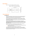
12 block diagram figure 3-1 shows a block diagram of the dstni i 2 c controller. Figure 3-1. Dstni i 2 c controller block diagram theory of operation i 2 c background the i 2 c bus is a popular serial, two-wire interface used in many systems because of its low overhead. Capable of 100 khz operation,...
Page 21
13 i 2 c controller the i 2 c controller base address is d000h and shares int2 with the spi controller. The i 2 c bus interface requires two bi-directional buffers with open collector (or open drain) outputs and schmitt inputs. Operating modes the following sections describe the possible i 2 c opera...
Page 22
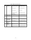
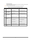
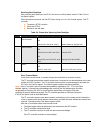
14 table 3-1. Master transmit status codes code i 2 c state microprocessor response next i 2 c action 18h addr + w transmitted, ack received 7-bit address: write byte to data, clear iflg or set sta, clear iflg or set stp, clear iflg or set sta & stp, clear iflg 10-bit address: write extended address...
Page 23
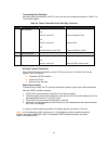
15 servicing the interrupt after servicing this interrupt, and transmitting the second part of the address, the status register contains one of the codes in table 3-2. Note: if a repeated start condition transmits, the status code is 10h instead of 08h. Table 3-2. Codes after servicing interrupts (m...
Page 24
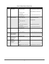
16 transmitting each data byte after each data byte transmits, the iflg is set, and one of the three status codes in table 3-3 is in the status register. Table 3-3. Status codes after each data byte transmits code i 2 c state microprocessor response next i 2 c action 28h data byte transmitted, ack r...
Page 25
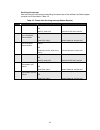
17 table 3-4. Master receive status codes code i 2 c state microprocessor response next i 2 c action 40h addr + w transmitted, ack received 7-bit address: clear iflg, aak=0 or clear iflg, aak=1 10-bit address: write extended address byte to data, clear iflg transmit data byte, receive not ack receiv...
Page 26
18 servicing the interrupt after servicing this interrupt and transmitting the second part of the address, the status register contains one of the codes in table 3-5. Table 3-5. Codes after servicing interrupt (master receive) code i 2 c state microprocessor response next i 2 c action 38h arbitratio...
Page 27
19 receiving each data byte after receiving each data byte, the iflg is set and one of three status codes in table 3-6 is in the status register. When all bytes are received, set the stp bit by writing a 1 to it in the control register. The i 2 c controller: transmits a stop condition clears the stp...
Page 28
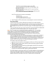
20 − the iflg is set and the status register contains b8h. − after the last transmission byte loads in the data register, clear aak when iflg clears. − after the last byte is transmitted, the iflg is set and the status register contains c8h. − the i 2 c controller returns to the idle state and the a...
Page 29
21 bus clock considerations bus clock speed the i 2 c bus can be defined for bus clock speeds up to 100 kb/s and up to 400 kb/s in fast mode. To detect start and stop conditions on the bus, the m i 2 c must sample the i 2 c bus at least 10 times faster than the fastest master bus clock on the bus. T...
Page 30
22 resetting the i 2 c controller there are two ways to reset the i 2 c controller. Using the rstin# pin writing to the software reset register using the rstin# pin reset method: clears the address, extended slave address, data, and control registers to 00h. Sets the status register to f8h. Sets the...
Page 31
23 i 2 c controller register definitions slave address register table 3-8. Slave address register bit 7 6 5 4 3 2 1 0 offset d000 extended address 1 1 1 1 0 slax9 slax8 general call address enable field sla6 sla5 sla4 sla3 sla2 sla1 sla0 gce reset 0 0 0 0 0 0 0 0 rw rw rw rw rw rw rw rw rw table 3-9...
Page 32
24 data register the data register contains the transmission data/slave address or the receipt data byte. In transmit mode, the byte is sent most-significant bits first. In receive mode, the first bit received is placed in the register’s most-significant bits. After each byte transmits, the data reg...
Page 33
25 control register table 3-12. Control register bit 7 6 5 4 3 2 1 0 offset d004 field ien enab sta stp iflg aak /// /// reset 0 0 0 0 0 0 0 0 rw rw rw rw rw rw rw rw rw table 3-13. Control register definitions bits field name description 7 ien extended slave address l = interrupt line (intr) goes h...
Page 34
26 bits field name description 2 aak acknowledge 1 = send acknowledge (low level on sda) during acknowledge clock pulse on the i 2 c bus if: −the entire 7-bit slave address or the first or second bytes of a 10-bit slave address are received. − the general call address is received and the gce bit in ...
Page 35
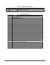
27 table 3-15. Status register definitions bits field name description 7:3 status code status code five-bit status code. See table 3-16. 2:0 /// reserved table 3-16. Status codes code description 00h bus error 08h start condition sent 10h repeated start condition sent 18h address + write bit sent, a...
Page 36
28 clock control register the clock control register is a write only register that contains seven least-significant bits. These least-significant bits control the frequency: at which the i 2 c bus is sampled. Of the i 2 c clock line (scl) when the i 2 c controller is in master mode. The cpu clock fr...
Page 37
29 extended slave address register table 3-19. Extended slave address register bit 7 6 5 4 3 2 1 0 offset d008 field slax7 slax6 slax5 slax4 slax3 slax2 slax1 slax0 reset 0 0 0 0 0 0 0 0 rw rw rw rw rw rw rw rw rw table 3-20. Extended slave address register definitions bits field name description 7 ...
Page 38
30 4 4 : : u u s s b b c c o o n n t t r r o o l l l l e e r r this chapter describes the dstni universal serial bus (usb) controller. Topics include: features on page 30 theory of operation on page 31 usb register summary on page 38 usb register definitions on page 39 host mode operation on page 50...
Page 39
31 theory of operation usb background usb is a serial bus operating at 12 mb/s. Usb provides an expandable, hot-pluggable plug- and-play serial interface that ensures a standard, low-cost socket for adding external peripheral devices. Usb allows the connection of up to 127 devices. Devices suitable ...
Page 40
32 microprocessor interface the usb microprocessor interface is made up of a slave interface and a master interface. The slave interface consists of a number of usb control and configuration registers. Usb internal registers can be accessed using a simple microprocessor interface. The master interfa...
Page 41
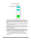
33 figure 4-1. Buffer descriptor table the microprocessor manages buffers intelligently for the usb by updating the bdt as necessary. This allows the usb to handle data transmission and reception efficiently while the microprocessor performs communication-overhead processing and other function-depen...
Page 42
34 table 4-1. Usb data direction rx tx device out or setup in host in out or setup addressing bdt entries before describing how to access endpoint data via the usb or microprocessor, it is important to understand the bdt addressing mechanism. The bdt occupies up to 256 bytes of system memory. Sixtee...
Page 43
35 table 4-4. Bdt data used by usb controller and microprocessor usb controller determines… microprocessor determines… who owns the buffer in system memory who owns the buffer in system memory data0 or data1 pid data0 or data1 pid release own upon packet completion no address increment (fifo mode) d...
Page 44
36 table 4-6. Usb buffer descriptor format definitions bits field name description 7 own bd owner specifies which unit has exclusive access to the bd. 0 = microprocessor has exclusive and entire bd access; usb ignores all other fields in the bd 1 = usb has exclusive bd access sie writes a 0 to this ...
Page 45
37 usb transaction when the usb transmits or receives data: 1. The usb uses the address generation in table 4-5 to compute the bdt address. 2. After reading the bdt, if the own bit equals 1, the sie dmas the data to or from the buffer indicated by the bd’s addr field. 3. When the token is complete, ...
Page 46
38 usb register summary table 4-7. Usb register summary hex offset mnemonic register description page 00 int_stat bits for each interrupt source in the usb. 39 02 err_stat bits for each error source in the usb. 41 04 stat transaction status in the usb. 43 06 addr usb address that the usb decodes in ...
Page 47
39 usb register definitions the following sections provide the usb register definitions. In these sections: the register mnemonic is provided for reference purposes. The register address shown is the address location of the register in the crb. The initialization value shown is the register’s initia...
Page 48
40 bits field name description 8 usb_rst enable/disable usb_rst interrupt 1 = enable the usb_rst interrupt. 0 = disable the usb_rst interrupt (default). 7 stall stall used in target and host modes. • in target mode, it asserts when the sie sends a stall handshake. • in host mode, it is set if the us...
Page 49
41 error register the error register contains bits for each of the error sources in the usb. Each of these bits is qualified with its respective error enable bits. The result is or’ed together and sent to the error bit of the interrupt status register. Once an interrupt bit has been set it may only ...
Page 50
42 bits field name description 5 dmaerr 1 = usb requests a dma access to read a new bdt, but is not given the bus before usb needs to receive or transmit data. • if processing a tx transfer, this causes a transmit data underflow condition. • if processing an rx transfer, this causes a receive data o...
Page 51
43 status register the status register reports the transaction status within the usb. When the microprocessor has received a tok_dne interrupt, the status register should be read to determine the status of the previous endpoint communication. The data in the status register is valid when the tok_dne...
Page 52
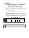
44 bits field name description 12 reset usb reset signal 1 = enables the usb to generate usb reset signaling. This allows the usb to reset usb peripherals. This control signal is only valid in host mode, (i.E., host_mdoe_en=1). Software must set reset to 1 for the required amount of time and then cl...
Page 53
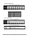
45 address register the address register contains the unique usb address that the usb decodes in peripheral mode (host_mode_en=0). In host mode (host_mode_en=1), the usb transmits this address with a token packet. This enables the usb to uniquely address any usb peripheral. In either mode the usb_en...
Page 54
46 frame number registers the frame number registers contain the 11-bit frame number. The current frame number is updated in these registers when a sof_token is received. Table 4-16. Frame number register bit 15 14 13 12 11 10 9 8 7 6 5 4 3 2 1 0 offset 08h field /// frm[10:0] reset 0 0 0 0 0 0 0 0 ...
Page 55
47 token register the token register performs usb transactions when in host mode (host_mode_en=1). When the host microprocessor wants to execute a usb transaction to a peripheral, it writes the token type and endpoint to this register. After this register is written, the usb begins the specified usb...
Page 56
48 table 4-18. Token register bit 15 14 13 12 11 10 9 8 7 6 5 4 3 2 1 0 offset 0ah sof threshold register token register field cnt[7:0] token_pid token_endpt reset 0 0 0 0 0 0 0 0 0 0 0 0 0 0 0 0 rw r/ w r/ w r/ w r/ w r/ w r/ w r/ w r/ w r/ w r/ w r/ w r/ w r/ w r/ w r/ w r/ w table 4-19. Token reg...
Page 57
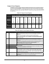
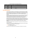
49 endpoint control registers the endpoint control registers contain the endpoint control bits for the 16 endpoints available on usb for a decoded address. These four bits define all the control necessary for any one endpoint. Endpoint 0 (endpt0) is associated with control pipe 0, which is required ...
Page 58
50 table 4-23. Endpoint control register definitions ep_ctl_dis ep_rx_en ep_tx_en endpoint enable / direction control /// 0 0 disable endpoint. /// 0 1 enable endpoint for tx transfer only. /// 1 0 enable endpoint for rx transfer only. 1 1 1 enable endpoint for rx and tx transfers. 0 1 1 enable endp...
Page 59
51 sample host mode operations figure 3. Enable host mode and configure a target device.
Page 60
52 figure 4. Full-speed bulk data transfers to a target device.
Page 61
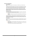
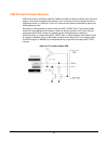
53 usb pull-up/pull-down resistors usb uses pull-up or pull-down resistors to determine when an attach or detach event occurs on the bus. Host mode complicates the resistors, since it requires devices to operate as either a usb target device or a usb host. Figure 4-5 shows the two resistor combinati...
Page 62
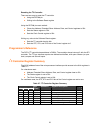
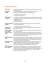
54 usb interface signals clock (clk) the clock input is required to be connected to a 12 mhz signal that is derived from the usb signals. Usp speed (speed) the usb speed indicator is used by external usb transceiver logic to determine which speed interface the usb is implementing. 1 = usb is operati...
Page 63
55 5 5 : : c c a a n n c c o o n n t t r r o o l l l l e e r r s s this chapter describes the dstni can controller. Topics include: canbus background on page 56 features on page 57 theory of operation on page 58 can register summaries on page 58 can register definitions on page 63 can bus interface ...
Page 64
56 canbus background can is a fast and highly reliable, multicast/multimaster, prioritized serial communications protocol that is designed to provide reliable and cost-effective links. Can uses a twisted-pair cable to communicate at speeds of up to 1 mb/s with up to 127 nodes. It was originally deve...
Page 65
57 canbus speed and length table 7-1 shows the relationship between the bit rate and cable length. Table 5-1. Bit rates for different cable lengths bit rate cable length 10 kb/s 6.7 km 20 kb/s 3.3 km 50 kb/s 1.3 km 125 kb/s 530 m 250 kb/s 270 m 500 kb/s 130 m 1 mb/s 40 m features three programmable ...
Page 66
58 theory of operation the can controller appears to the microprocessor as an i/o device. Each peripheral has 256 bytes of i/o address space allocated to it. Can0 and can1 share interrupt 6. Table 5-2. Can i/o address can controller base address can0 a800h can1 a900h can register summaries dstni con...
Page 67
59 hex offset register 30 rxmessage: id, id28-13 32 id12-00 34 rxmessage: data, d55-48, d63-56 36 d39-32, d47-40 38 d23-16, d31-24 3a d07-00, d15-08 3c rxmessage: rtr, ide, dlc_3-0,afi_2-0 3e rxmessage: control flags, fifo_lvl_2-0, msgaval 40 transmitter and receive error counter 42 error status 44 ...
Page 68
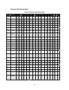
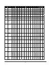
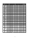
60 detailed can register map table 5-4. Detailed can register map hex offset register 15 14 13 12 11 10 9 8 7 6 5 4 3 2 1 0 0x00 tx msg 0 id28 id27 id26 id25 id24 id23 id22 id21 id20 id19 id18 id17 id16 id15 id14 id13 0x02 /// id12 id11 id10 id09 id08 id07 id06 id05 id04 id03 id02 id01 id00 /// /// ...
Page 69
61 hex offset register 15 14 13 12 11 10 9 8 7 6 5 4 3 2 1 0 0x30 rx msg id28 id27 id26 id25 id24 id23 id22 id21 id20 id19 id18 id17 id16 id15 id14 id13 0x32 /// id12 id11 id10 id09 id08 id07 id06 id05 id04 id03 id02 id01 id00 /// /// /// 0x34 /// d55 d54 d53 d52 d51 d50 d49 d48 d63 d62 d61 d60 d59 ...
Page 70
62 hex offset register 15 14 13 12 11 10 9 8 7 6 5 4 3 2 1 0 0x52 acceptance mask register 0 id28 id27 id26 id25 id24 id23 id22 id21 id20 id19 id18 id17 id16 id15 id14 id13 0x54 /// id12 id11 id10 id09 id08 id07 id06 id05 id04 id03 id02 id01 id00 ide rtr /// 0x56 /// d55 d54 d53 d52 d51 d50 d49 d48 ...
Page 71
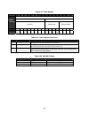
63 can register definitions tx message registers to avoid priority inversion issues in the transmit path, three transmit buffers are available with a built-in priority arbiter. When a message is transmitted, the priority arbiter evaluates all pending messages and selects the one with the highest pri...
Page 72
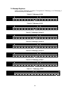
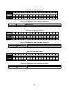
64 tx message registers table 5-5 shows txmessage_0 registers. The registers for txmessage_1 and txmessage_2 are identical except for the offsets. Table 5-5. Txmessage_0:id28 bit 15 14 13 12 11 10 9 8 7 6 5 4 3 2 1 0 offset 00h field id28 id27 id26 id25 id24 id23 id22 id21 id20 id19 id18 id17 id16 i...
Page 73
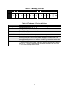
65 table 5-12. Txmessage_0:ctrl flags bit 15 14 13 12 11 10 9 8 7 6 5 4 3 2 1 0 offset 0e field /// /// /// /// /// /// /// /// /// /// /// /// /// /// tx abort trx table 5-13. Txmessage_0 register definitions field name description id_28:id_0 message identifier for both standard and extended messag...
Page 74
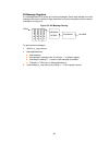
66 rx message registers a 4-message-deep fifo stores the incoming messages. Status flags indicate how many messages are stored. Additional flags determine from which acceptance filter the actual message is coming from. Figure 5-2. Rx message routing rx m es sage 1 message filters can module up bus c...
Page 75
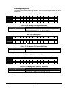
67 rx message registers the following table shows rxmessage registers. See the complete register table at the start of this section. Table 5-14. Rxmessage:id28 bit 15 14 13 12 11 10 9 8 7 6 5 4 3 2 1 0 offset 30h field id28 id27 id26 id25 id24 id23 id22 id21 id20 id19 id18 id17 id16 id15 id14 id13 r...
Page 76
68 table 5-20. Rx message: data 39 bit 15 14 13 12 11 10 9 8 7 6 5 4 3 2 1 0 offset 36h field d39 d38 d37 d36 d35 d34 d33 d32 d47 d46 d45 d44 d43 d42 d41 d40 reset 0 0 0 0 0 0 0 0 0 0 0 0 0 0 0 0 r/w r/w r/w r/w r/w r/w r/w r/w r/w r/w r/w r/w r/w r/w r/w r/w r/w table 5-21. Rx message: data 39 regi...
Page 77
69 table 5-26. Rxmessage: rtr bit 15 14 13 12 11 10 9 8 7 6 5 4 3 2 1 0 offset 3c field /// afi_2 afi_1 afi_0 /// rtr ide dlc_3 dlc_2 dlc_1 dlc_0 reset 0 0 0 0 0 0 0 0 0 0 0 0 0 0 0 0 r/w r/w r/w r/w r/w r/w r/w r/w r/w r/w r/w r/w r/w r/w r/w r/w r/w table 5-27. Rx message: rtr register definitions...
Page 78
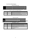
70 error count and status registers table 5-30. Tx/rx error count bit 15 14 13 12 11 10 9 8 7 6 5 4 3 2 1 0 offset 40h field re7 re6 re5 re4 re3 re2 re1 re0 te7 te6 te5 te4 te3 te2 te1 te0 reset 0 0 0 0 0 0 0 0 0 0 0 0 0 0 0 0 r/w r/w r/w r/w r/w r/w r/w r/w r/w r/w r/w r/w r/w r/w r/w r/w r/w table...
Page 79
71 table 5-34. Tx/rx message level register bit 15 14 13 12 11 10 9 8 7 6 5 4 3 2 1 0 offset 44h field /// rl1 rl0 tl1 tl0 reset 0 0 0 0 0 0 0 0 0 0 0 0 0 0 0 0 r/w r/w r/w r/w r/w r/w r/w r/w r/w r/w r/w r/w r/w r/w r/w r/w r/w table 5-35. Tx/rx message level register definitions bits field name de...
Page 80
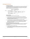
72 interrupt flags the following flags are set on internal events (they activate an interrupt line when enabled). They are cleared by writing a ‘ 1’ to the appropriate flag. Acknowledging the tx_msg interrupt also acknowledges all tx_xmit interrupt sources. Acknowledging one of the tx_xmit interrupt...
Page 81
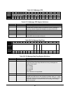
73 interrupt enable registers all interrupt sources are grouped into three groups (traffic, error and diagnostics interrupts). To enable a particular interrupt, set its enable flag to ‘ 1’ . Table 5-38. Interrupt enable registers bit 15 14 13 12 11 10 9 8 7 6 5 4 3 2 1 0 offset 48h field rx_msg tx_m...
Page 82
74 bits field name description 3 ovr_load overload condition − int3n group (diagnostic interrupts) 1 = enable flag set. 0 = enable flag not set. 2 arb_loss arbitration loss − int3n group (diagnostic interrupts) 1 = enable flag set. 0 = enable flag not set. 1 /// reserved 0 int_enb general interrupt ...
Page 83
75 figure 5-3. Can operating mode can module 1 can module 2 a c b d can port 1 can port 2 dstni note: the loopback mode register in can module 2 is not functional. For proper operation in loopback mode, the configuration of both can modules must be the same. Can configuration registers the following...
Page 84
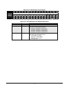
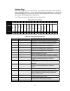
76 table 5-44. Configuration register bit 15 14 13 12 11 10 9 8 7 6 5 4 3 2 1 0 offset 4eh field ov r_ms g ts2_2 ts2_1 ts2_0 ts1_3 ts1_2 ts1_1 ts1_0 /// auto _res cfg_sjw1 samp_mo d e d ge _mod reset 0 0 0 0 0 0 0 0 0 0 0 0 0 0 0 0 r/w r/w r/w r/w r/w r/w r/w r/w r/w r/w r/w r/w r/w r/w r/w r/w r/w ...
Page 85
77 the following relations exist for bit time, time quanta, time segments ½, and the data sampling point. Figure 5-4. Bit time, time quanta, and sample point relationships bit time 1 tseg1 + 1 tseg2 + 1 time quanta (tq) sample point bittime = (1+ ( tseg1 + 1) + (tseg2 + 1)) x timequanta timequanta =...
Page 86
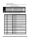
78 acceptance filter and acceptance code mask three programmable acceptance mask and acceptance code register (amr/acr) pairs filter incoming messages. The acceptance mask register (amr) defines whether the incoming bit is checked against the acceptance code register (acr). Table 5-46. Acceptance fi...
Page 87
79 table 5-50. Acceptance mask register: id 12 bit 15 14 13 12 11 10 9 8 7 6 5 4 3 2 1 0 offset 54h field id12 id11 id10 id09 id08 id07 id06 id05 id04 id03 id02 id01 id00 ide rtr /// reset 0 0 0 0 0 0 0 0 0 0 0 0 0 0 0 0 r/w r/w r/w r/w r/w r/w r/w r/w r/w r/w r/w r/w r/w r/w r/w r/w r/w table 5-51....
Page 88
80 table 5-54. Acceptance code register bit 15 14 13 12 11 10 9 8 7 6 5 4 3 2 1 0 offset 58h field id28 id27 id26 id25 id24 id23 id22 id21 id20 id19 id18 id17 id16 id15 id14 id13 reset 0 0 0 0 0 0 0 0 0 0 0 0 0 0 0 0 r/w r/w r/w r/w r/w r/w r/w r/w r/w r/w r/w r/w r/w r/w r/w r/w r/w table 5-55. Acc...
Page 89
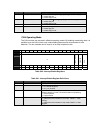
81 canbus analysis three additional registers are provided for advanced analysis of a can system. These registers include arbitration lost and error capture registers, as well as a canbus frame reference register that contains information about the canbus state and the physical rx and tx pins. Arbit...
Page 90
82 error capture register the error capture register captures the most recent error event with the frame reference pointer, rx- and tx-mode and the associated error code. Table 5-62. Error capture register bit 15 14 13 12 11 10 9 8 7 6 5 4 3 2 1 0 offset 78h field err2 err1 err0 fr4 fr3 fr2 fr1 fr0 ...
Page 91
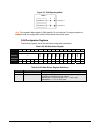
83 frame reference register the frame reference register contains information of the current bit of the can message. A frame reference pointer indicates the current bit position. This enables message tracing on bit level. Note: the reset value of this register’s bits is indeterminate. Table 5-64. Fr...
Page 92
84 bits field name description 5:0 frb[5:0] frame_ref_bit_nr a 6-bit vector that counts the bit numbers in one field. Example: if field = “data” = “01010”, “bit_nr” = “000000”, and “tx_mode” = ‘1’, it indicates that the first data bit is being transmitted. Can bus interface dstni contains two comple...
Page 93
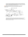
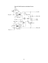
85 you can also provide local isolated power for the transceiver circuits, as required when using canopen. If you are using both devicenet and canopen, use the jumpers to select between bus power (+5_bus) or isolated power (iso_pwr). The jumpers p_c05v and p_c0g will then provide +5_can and gnd_can ...
Page 94
86 figure 5-8. Can transceiver and isolation circuits +5_can 1 u6 hcpl-o601 vcc gnd 8 5 c67 0.01uf r191 680 7 +3.3v 2 r193 270 can_tx 3 4 +5_can 470 6 rxd 4 txd u18 pca82c251 canl canh 6 can- 7 can+ c10 0.01uf gnd_can 3 v+ 8 2 gnd_can gnd rs 1 gnd_can c9 0.01uf 1 vcc gnd 8 5 c12 0.01uf r190 680 7 +5...
Page 95
87.

