- DL manuals
- Lattice Semiconductor
- Motherboard
- ECP5-5G
- User Manual
Lattice Semiconductor ECP5-5G User Manual
Summary of ECP5-5G
Page 1
Ecp5-5g™ versa development board user guide eb103 version 1.2, january 2016.
Page 2
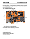
2 ecp5-5g versa development board introduction the ecp5-5g™ versa development board allows designers to investigate and experiment with the features of the ecp5-5g field-programmable gate array. The features of the ecp5-5g versa development board can assist engineers with rapid prototyping and testi...
Page 3
3 ecp5-5g versa development board the contents of this user guide include top-level functional descriptions of the various portions of the evaluation board, descriptions of the on-board connectors, diodes and switches and a complete set of schematics. Caution: the ecp5-5g versa development board con...
Page 4
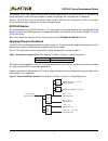
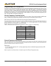
4 ecp5-5g versa development board programming/fpga configuration the ecp5-5g versa development board has a built-in download controller for programming the ecp5-5g fpga. The built-in module consists of a usb type-b connector and a usb uart device. To use the built-in download cable, simply connect a...
Page 5
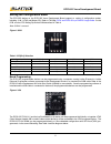
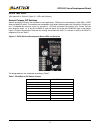
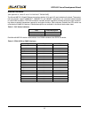
5 ecp5-5g versa development board setting the configuration mode the ecp5-5g device on the ecp5-5g versa development board supports a variety of configuration modes, including 1149.1 jtag and master spi. Refer to tn1260, ecp5 and ecp5-5g sysconfig usage guide . On the pcb, use the cfg setting dip sw...
Page 6
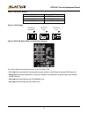
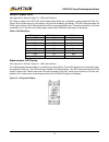
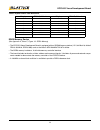
6 ecp5-5g versa development board table 4. Jtag chain selector j50 shunts jtag chain 1-2, 3-4, 5-6 ecp5-5g + ispclock 1-2, 3-5 ecp5-5g only 2-4, 5-6 ispclock only figure 5. J50 settings ecp5-5g + ispclock ecp5-5g only ispclock only figure 6. Ecp5-5g status leds and push-button controls the leds indi...
Page 7
7 ecp5-5g versa development board programn and gsrn these push-button switches assert/de-assert the logic levels on programn (sw2) and gsrn (sw1). Depress- ing the button drives a logic level “0” to the device. Programming serial spi flash memory a serial spi (16-pin tssop, 128m) flash memory device...
Page 8
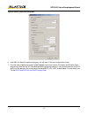
8 ecp5-5g versa development board figure 8. Device properties dialog box 6. Click ok in the device properties dialog box. You will return to the main configuration screen. 7. From the main programming window, select program from the top toolbar. This begins the spi serial flash programming. Note tha...
Page 9
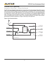
9 ecp5-5g versa development board on-board clock capabilities (see appendix a, sheet 9, figure 21 - reference clock generator) the ecp5-5g versa development board allows for several clock source options. Some of these options are con- trolled via the ispclock5406d programmable clock manager device. ...
Page 10
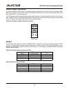
10 ecp5-5g versa development board general purpose clock source an on-board 100 mhz lvds oscillator is provided for general purpose use. This clock source is connected to differ- ential inputs p3 and p4 and must be used as lvds inputs to the fpga. This pin pair also provides optimal inter- face to t...
Page 11
11 ecp5-5g versa development board fpga test pins (see appendix a, sheet 8, figure 20 - leds and switches) general purpose dip switches general purpose fpga pins are available for user applications. Fpga pins are connected to switch sw3, a spst slide-actuated dip switch. The switches are connected t...
Page 12
12 ecp5-5g versa development board general purpose leds (see appendix a, sheet 8, figure 20 - leds and switches) the leds provided on the ecp5-5g versa development board are connected to general purpose fpga i/os. These leds provide status for user designs and must be included in the design. The led...
Page 13
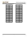
13 ecp5-5g versa development board table 9. Alpha-numeric led definitions display fpga ball number display fpga ball number a m20 j n18 b l18 k p17 c m19 l n17 d l16 m p16 e l17 n r16 f m18 p r17 g n16 dp u1 h m17 ddr3 memory device (see appendix a, sheet 7, figure 19 - ddr3 memory) • the ecp5-5g ve...
Page 14
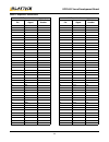
14 ecp5-5g versa development board table 10. Ddr3 memory controller interconnections ddr3 signal fpga ball number ddr3 signal fpga ball number dq0 l5 a0 p2 dq1 f1 a1 c4 dq2 k4 a2 e5 dq3 g1 a3 f5 dq4 l4 a4 b3 dq5 h1 a5 f4 dq6 g2 a6 b5 dq7 j3 a7 e4 dq8 d1 a8 c5 dq9 c1 a9 e3 dq10 e2 a10 d5 dq11 c2 a11 ...
Page 15
15 ecp5-5g versa development board ethernet interfaces (see appendix a, sheets 5 and 6 "10/100/1000-t phy#x/rj45") two marvell 88e1512 gigabit ethernet transceiver devices (u14 and u15) are included on the board. These phys- ical layer devices support 1000base-t, 100base-tx, and 10base-t application...
Page 16
16 ecp5-5g versa development board table 13. Expansion connections x3 expansion connector x4 expansion connector pin signal fpga ball number pin signal fpga ball number 1 gnd — 1 resout# a8 2 nc — 2 gnd — 3 2v5 — 3 io0 a12 4 io29 b19 4 io1 a13 5 io30 b12 5 io2 b13 6 io31 b9 6 io3 c13 7 io32 e6 7 io4...
Page 17
17 ecp5-5g versa development board references • ds1057, ecp5-5g family data sheet • ug112, pci express demos for the ecp5-5g versa development board • ug111, 5.0 gpbs serdes eye demo for the ecp5-5g versa development board ordering information description ordering part number china rohs environment-...
Page 18
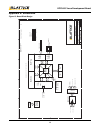
18 ecp5-5g versa development board appendix a. Schematics figure 13. Board block design 5 5 4 4 3 3 2 2 1 1 d d c c b b a a power device power pins programming 3.3v spi pcsa bank 8 ecp5 bank 0 bank 3 fpga bank 6 bank 7 bank 1 bank 2 serdes designator u1 is the fpga dut. Pcie x1 ch#0 clk5406 referenc...
Page 19
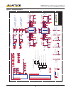
19 ecp5-5g versa development board figure 14. Voltage regulators 5 5 4 4 3 3 2 2 1 1 d d c c b b a a core po w er 0.45 v drop at 500 ma max +1.5v 1.1 a po w er i n put +11 v to +16 v 1.2 v /m s 1.2 v /m s 1.2 v /m s v oltage reg u lator s +3.3 v 1.35 a sw 3_3v, +3.3 v, 1.35 a po w er s u ppl y block...
Page 20
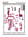
20 ecp5-5g versa development board figure 15. Programming 5 5 4 4 3 3 2 2 1 1 d d c c b b a a fpga gsrn programn done indicator will light when configuration is successfully completed initn indicator will light if an error occurs during configuration programming config status leds programn & gsrn pu...
Page 21
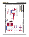
21 ecp5-5g versa development board figure 16. Serdes 5 5 4 4 3 3 2 2 1 1 d d c c b b a a x1 pcie board fingers all nets to smas are 100-ohm differential pairs. The p and n traces shall be all nets are 85-ohm differential pairs. The p and n traces shall be b side = primary component side(top) a side ...
Page 22
22 ecp5-5g versa development board figure 17. 10/100/1000-t phy #1/rj45 5 5 4 4 3 3 2 2 1 1 d d c c b b a a mh1 and mh2 are 0.100" diam eter plated thro u gh holes ethernet rj45 connector place caps close to rj45 jack place termination resistors rx_d0-3, rx_clk, tx_clk, as close to the g-phy as poss...
Page 23
23 ecp5-5g versa development board figure 18. 10/100/1000-t phy #2/rj45 5 5 4 4 3 3 2 2 1 1 d d c c b b a a mh1 and mh2 are 0.100" diam eter plated thro u gh holes ethernet rj45 connector place caps close to rj45 jack place termination resistors rx_d0-3, rx_clk, tx_clk, as close to the g-phy as poss...
Page 24
24 ecp5-5g versa development board figure 19. Ddr3 memory 5 5 4 4 3 3 2 2 1 1 d d c c b b a a all memory controller buses, clocks, and control traces must be 50 ohm transmission lines place close to memory chip place address/control termination resistors as close as possible to memory chip u7 vtt x1...
Page 25
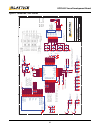
25 ecp5-5g versa development board figure 20. Leds and switches 5 5 4 4 3 3 2 2 1 1 d d c c b b a a 14-segment display dip switch leds dp p n m l k j g h f e d c b a character si g nal ma p seg14 seg13 seg12 seg11 seg10 seg9 seg 8 seg6 seg7 seg5 seg4 seg3 seg2 seg1 seg0 u1 r17 r16 p16 n17 p17 n1 8 n...
Page 26
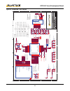
26 ecp5-5g versa development board figure 21. Reference clock generator 5 5 4 4 3 3 2 2 1 1 d d c c b b a a place b y pass caps close to o u tp u t b ank s u pply pins. R e fclkp_d0 re fclk n _d0 v cco p c ie _clkp p c ie _clk n c l k_r eset n clk _lock 1 cl k _ v cc c l k_sc l c l k_sd a v cco ispc...
Page 27
27 ecp5-5g versa development board figure 22. Expansion connector 5 5 4 4 3 3 2 2 1 1 d d c c b b a a pin 2 removed for coding of expansion board 5vin gnd schematic symbols rev 4.1 schematic symbols rev 4.1 bank 0 bank 1 expc o n _i o30 expc o n _i o32 expc o n _i o34 expc o n _i o36 expc o n _i o3 ...
Page 28
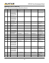
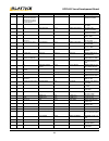
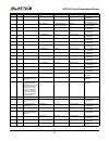
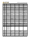
28 ecp5-5g versa development board appendix b. Bill of materials table 14. Ecp5-5g versa development board bill of materials item quantity reference part manufacturer part number description 1 1 cn1 pci express x1 edge finger conn. 2 31 c1,c2,c3,c4,c5,c20,c21, c29,c33,c85,c89,c92, c95,c108,c110,c113...
Page 29
29 ecp5-5g versa development board 22 19 c182,c184,c187,c190, c192,c194,c196,c198, c200,c204,c217,c219, c221,c223,c226,c228, c234,c236,c241 10nf-0603smt kemet c0603c103k5ractu cap .01 uf 50 v ceramic x7r 0603 23 1 c229 6.8uf-tan-0805smt kemet t494r685k006as cap tant 6.8 uf 6.3 v 10% smd 24 1 c235 56...
Page 30
30 ecp5-5g versa development board 54 1 rn7 exb2hv221jv panasonic exb2hv221jv res array 220 ohm 5% 8 res smd 55 1 rn9 exb2hv472jv panasonic exb2hv472jv res array 4.7k ohm 5% 8 res smd 56 1 rp1 cts-rt1402b7 cts corporation resis- tor/electrocomponents rt2402b7 res net ddr sdram 50 ohm 3x9 bga 57 4 r6...
Page 31
31 ecp5-5g versa development board 81 5 r63,r64,r66,r67,r70 0.1 vishay dale wsl2010r1000fea res .1 ohm 1/2 w 1% 2010 smd 82 2 r71,r75 2_2k-0603smt-dni dni 83 5 r73,r74,r107,r108,r156 100r-0402smt panasonic erj-2rkf1000x res 100 ohm 1/10 w 1% 0402 smd 84 1 r76 0r-0603smt-dni dni 85 4 r85,r99,r111,r11...
Page 32
32 ecp5-5g versa development board 112 1 u12 lp2998-so8 national lp2998max/nopb termination regulator 113 1 u13 ispclock5406d lattice supplied isppac-clk5406d- 01sn48i 114 2 u14,u15 88e1512_56qfn marvell 88e1512-a0-nnp2c000 single-port eee gigabit ether 115 2 u44,u45 r0_1-3 panasonic erj-3gey0r00v r...


