Summary of ECP5
Page 1
July 2014 eb91_1.0 ecp5™ pci express board user’s guide.
Page 2
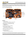
2 ecp5 pci express board user’s guide introduction the ecp5™ pci express board allows designers to investigate and experiment with the features of the ecp5 field-programmable gate array. The features of the ecp5 pci express board can assist engineers with rapid pro- totyping and testing of their spe...
Page 3
3 ecp5 pci express board user’s guide caution: the ecp5 pci express board contains esd-sensitive components. Esd safe practices should be fol- lowed while handling and using the evaluation board. Ecp5 device this board features an ecp5 fpga in a 756-ball cabga with a 1.1 v core supply. A complete de...
Page 4
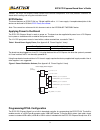
4 ecp5 pci express board user’s guide your pc (with diamond programmer software installed). The usb hub on the pc will detect the addition of the usb function, making the built-in cable available for use with the diamond programmer software. Diamond programmer requirements note: this board includes ...
Page 5
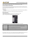
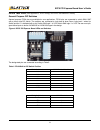
5 ecp5 pci express board user’s guide figure 4. Ecp5 configuration pin (cfg pins) figure 5. Ecp5 status leds and push-button controls the leds indicate the configuration status of the ecp5 fpga. • d10 (red) illuminated indicates that programming was aborted or reinitialized, driving the initn output...
Page 6
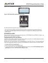
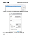
6 ecp5 pci express board user’s guide figure 6. Device information dialog screen 4. Under the spi flash options, select family to spi serial flash, vendor to micron, device to spi-n25q128a, package to 16-lead soic. Figure 7. Select device dialog box 5. Click ok in the device properties dialog box. Y...
Page 7
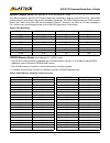
7 ecp5 pci express board user’s guide on-board clock capabilities (see appendix b, "clock generation" and "lpddr3" sheets) the ecp5 pci express board allows for several clock source options. Some of these options are controlled via the ispclock5304 programmable clock manager device. The clock manage...
Page 8
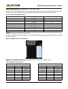
8 ecp5 pci express board user’s guide fpga test pins (see appendix b, "ecp5 config" and "leds and switches" sheets) general purpose dip switches general purpose fpga pins are available for user applications. Fpga pins are connected to switch sw4, sw7 with a piano style dip switch. The switches are c...
Page 9
9 ecp5 pci express board user’s guide general purpose leds (see appendix b, "leds and switches" sheet) the leds provided on the ecp5 pci express board are connected to general purpose fpga i/os. These leds provide status for user designs and must be included in the design. The leds illuminate when t...
Page 10
10 ecp5 pci express board user’s guide ethernet interfaces (see appendix b, "rj45" sheet) one marvell 88e1512 gigabit ethernet transceiver device (u11) is included on the board. This physical layer device supports 1000base-t, 100base-tx, and 10base-t applications via a standard media interface to a ...
Page 11
11 ecp5 pci express board user’s guide power measurements (see appendix b, "ecp5 power" sheet) the ecp5 pci express board allows for easy power measurements with a multi-meter of the ecp5 device. The ecp5 power rails are isolated and can be measured by measuring the voltage across power resistors. F...
Page 12
12 ecp5 pci express board user’s guide 9 lvcmos1_7 d15 9 lvcmos2_7 d20 10 lvcmos1_5 f16 10 lvcmos2_5 f19 11 lvcmos1_10 b14 11 lvcmos2_10 a22 12 lvcmos1_8 a14 12 lvcmos2_8 c20 13 lvcmos1_11 c14 13 lvcmos2_11 c22 14 lvcmos1_9 f15 14 lvcmos2_9 f20 15 lvcmos1_14 f14 15 lvcmos2_14 e22 16 lvcmos1_12 e14 1...
Page 13
13 ecp5 pci express board user’s guide ordering information description ordering part number china rohs environment- friendly use period (efup) ecp5 pci express board lfe5um-85f-pb-evn technical support assistance e-mail: techsupport@latticesemi.Com internet: www.Latticesemi.Com revision history apr...
Page 14
14 ecp5 pci express board user’s guide appendix a. Bill of materials project name: ecp5 pci express board pac no: 305-pd-14-0xxx customer name: lattice date: 07-17-2014 rev:b item reference qty part pcb footprint comments part_number manufacturer description 1 cn1 1 card 1 pcie_edge_ finger - - - 2 ...
Page 15
15 ecp5 pci express board user’s guide 19 c89,c91,c96,c18 8,c189,c190,c20 2,c231,c235,c23 6,c279,c294,c29 5,c296,c297,c29 8,c301,c302,c30 4,c308,c309,c31 0,c318,c327,c32 9,c345,c348,c35 8,c361,c364,c36 5,c366,c367,c36 8,c369,c370,c37 1,c372,c373,c37 5,c376,c377,c37 8,c379,c380,c38 1,c382,c383,c38 4,...
Page 16
16 ecp5 pci express board user’s guide 49 l1,l2,l3,l4 4 4.7uh-cdrh5d cdrh5d customer sup- plied cdrh5d28rhpn p-4r7nc sumida inductor 4.7uh 25% smd 50 l5 1 600ohm 500ma fb0603 - blm18ag601sn1 d murata electronics north america ferrite chip 600 ohm 500ma 0603 51 q7,q8,q9,q10 4 2n2222 sm_sot23-3 - mmbt...
Page 17
17 ecp5 pci express board user’s guide 65 r106,r416, r417 3 220 r0603 - erj-3ekf2200v panasonic ecg res 220 ohm 1/10w 1% 0603 smd 66 r108,r190,r191, r192,r193,r194, r195,r196,r197 9 470 r0603 - erj-3ekf4700v panasonic ecg res470ohm1/10w1% 67 r109,r88 2 1k r0603 - crcw06031k00f kea vishay/dale resist...
Page 18
18 ecp5 pci express board user’s guide 96 tp3,tp4,tp5, tp7,tp8,tp9, tp10,tp11,tp12, tp13,tp14,tp15, tp16,tp17,tp18, tp19,tp20,tp21, tp22,tp23,tp24, tp25,tp26,tp27, tp28,tp29,tp30, tp31,tp32,tp33, tp34,tp35,tp36, tp37,tp38,tp39, tp40,tp41,tp42, tp43,tp44,tp45, tp46,tp47,tp48, tp49,tp50,tp51, tp52,tp5...
Page 19
19 ecp5 pci express board user’s guide appendix b. Schematic 5 5 4 4 3 3 2 2 1 1 d d c c b b a a ecp5 pci express board june 2014 revision: b date: size schematic rev of sheet title lattice semiconductor applications email: techsupport@latticesemi.Com board rev project nov, 2012 b b 28 1 cover page ...
Page 20
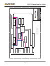
20 ecp5 pci express board user’s guide 5 5 4 4 3 3 2 2 1 1 d d c c b b a a configuration options (pg 9) ecp5-85 (pg 6,7,10, 19,20,23) usb port (pg 8) connector #1 (pg 13) connector #2 (pg 14) ethernet (pg 17) lpddr3 (pg 18) connector pcie 4 lane (pg 16) clocking (pg 12) pmod (pg 10) leds, switches (...
Page 21
21 ecp5 pci express board user’s guide 5 5 4 4 3 3 2 2 1 1 d d c c b b a a ecp5-85 bank 0 vccio=2.5v lvcmos, i2c bank 1 vccio=2.5v lvcmos, rgmii bank 2 vccio=1.5v mipirx bank 4 vccio=2.5v dip, led, spi cntrl bank 3 vccio=2.5v mipitx, difftx, diffrx bank 6 vccio=1.2v mipitxlp, lpddr3 bank 7 vccio=2.5...
Page 22
22 ecp5 pci express board user’s guide 5 5 4 4 3 3 2 2 1 1 d d c c b b a a date: si ze sc h e m a ti c r e v of sh e e t ti tl e l a tt ic e s e mic o n d u c tor a p pl ic at io ns e m a il : te c h s u ppor t@ lat ti c es em i. C o m b o ar d re v pr o je c t n o v, 2 0 1 2 b a 2 8 4 me c h a n ic...
Page 23
23 ecp5 pci express board user’s guide 5 5 4 4 3 3 2 2 1 1 d d c c b b a a core power 2.3v minimum input voltage 0.46 v drop at 500 ma max +1.5v 1.1 a power input +11v to +16v 1.2v/ms 1.2v/ms 1.2v/ms voltage regulators +3.3 v 1.35 a sw 3_3v, +3.3 v, 1.35 a power supply block diagram 12_0v +1.1 v 1.3...
Page 24
24 ecp5 pci express board user’s guide 5 5 4 4 3 3 2 2 1 1 d d c c b b a a vccaux current vcc current vcca current vccio2_5v current vccio1_5v current serdes current t n er r u c v 2 _ 1 oi c c v t n er r u c v 3 _ 3 oi c c v note: place ground test points around the board ground test points vccaux2...
Page 25
25 ecp5 pci express board user’s guide 5 5 4 4 3 3 2 2 1 1 d d c c b b a a board logos board mounting holes date: size schematic rev of sheet title lattice semiconductor applications email: techsupport@latticesemi.Com board rev project nov, 2012 b b 28 7 ecp5 gnds, xres, mounting, logos pci express ...
Page 26
26 ecp5 pci express board user’s guide 5 5 4 4 3 3 2 2 1 1 d d c c b b a a m93c46-wmn6tp manuf:st micro digi-key part number 497-5090-1-nd usb connection eesk eedata shld_debug eecs vcc18ft 3_3v 3_3v 3_3v 3_3v 3_3v 3_3v ftdi_tdi [pg9] ftdi_tck [pg9] ftdi_tdo [pg9] adbus4 [pg9] ftdi_tms [pg9] adbus7 ...
Page 27
27 ecp5 pci express board user’s guide 5 5 4 4 3 3 2 2 1 1 d d c c b b a a 4mbit spi for xo2 dual boot xo2 jtag jtag connections to devices jtag chain select sw6[4:1] jtag chain [0,0,0,1] xo2 [0,0,0,0] ecp5 [0,0,1,0] card1 [0,1,0,0] card2 [1,0,0,0] ispclock xo2_spi_in xo2_spi_out xo2_spi_cs0 xo2_spi...
Page 28
28 ecp5 pci express board user’s guide 5 5 4 4 3 3 2 2 1 1 d d c c b b a a programn part number:evq q2k03w panasonic smd dip switch done indicator will light when configuration is successfully completed r ot c e n n o c d o m p s d e l s ut at s gi f n o c initn indicator will light if an error occu...
Page 29
29 ecp5 pci express board user’s guide 5 5 4 4 3 3 2 2 1 1 d d c c b b a a dip switch leds sw# bga 1 ak31 2 am31 3 aj31 4 al32 5 ag28 6 aj28 7 ag29 8 ah28 led# bga 1 am28 2 al28 3 am29 4 ak28 5 ak32 6 am30 7 aj32 8 al30 2_5v 2_5v led1 [pg19] led2 [pg19] led3 [pg19] led4 [pg19] led5 [pg19] led6 [pg19...
Page 30
30 ecp5 pci express board user’s guide 5 5 4 4 3 3 2 2 1 1 d d c c b b a a system clock generation system 54mhz clock clk54-exta => ad32 lrc_gpll0t_in clk54-extb => a17 pclkt0_1 clk54a => card #1 clk54b => card #2 external clock source clock destinations all clock routing should be 50 ohm 50 ohm clo...
Page 31
31 ecp5 pci express board user’s guide 5 5 4 4 3 3 2 2 1 1 d d c c b b a a use 85-ohm traces for differential pairs. The p and n traces shall be b side = primary component side(top) a side = secondary component side(bottom) 54mhz osc clk mipi rx 1 clock pair 4 data pairs spi bus serdes diff rx/tx 2x...
Page 32
32 ecp5 pci express board user’s guide 5 5 4 4 3 3 2 2 1 1 d d c c b b a a b side = primary component side(top) a side = secondary component side(bottom) #2 proto use 85-ohm traces for differential pairs. The p and n traces shall be to avoid damage do not plug cn2 into pcie slots #2 54mhz osc clk mi...
Page 33
33 ecp5 pci express board user’s guide 5 5 4 4 3 3 2 2 1 1 d d c c b b a a all nets are 85-ohm differential pairs. The p and n traces shall be resistor switches (resistors with a shared pad) place near ecp5 from d0 through internal logic default connection is to pcie fp_pcsc_hdoutp0 fp_pcsc_hdoutn0 ...
Page 34
34 ecp5 pci express board user’s guide 5 5 4 4 3 3 2 2 1 1 d d c c b b a a b side = secondary component side(bottom) a side = primary component side(top) 4-lane pcie board fingers ac coupling x4_perp2 x4_pern2 x4_perp1 x4_pern1 x4_pern0 x4_perp0 x4_perp0 x4_pern0 x4_pern1 x4_perp1 x4_perp2 x4_perp3 ...
Page 35
35 ecp5 pci express board user’s guide 5 5 4 4 3 3 2 2 1 1 d d c c b b a a place termination resistors rx_d0-3, rx_er, rx_dv, rx_clk, tx_clk, crs, col, rstn as close to the g-phy as possible using 50 ohm impedence traces. Place termination resistors tx_d0-3, tx_er, tx_en, gtx_clk as close to fpga as...
Page 36
36 ecp5 pci express board user’s guide 5 5 4 4 3 3 2 2 1 1 d d c c b b a a all memory controller buses, clocks, and control traces must be 50 ohm transmission lines lpddr3 reference voltages (resistor option) lpddr3 100mhz lvds clock lvds signal matched length 100 ohm traces place close to memory ch...
Page 37
37 ecp5 pci express board user’s guide 5 5 4 4 3 3 2 2 1 1 d d c c b b a a part number:evq q2k03w panasonic smd fpga gsrn virtual power pushbtngsrn virvccio0 virvccio1 virgnd pushbtngsrn vccio2_5v vccio2_5v 2_5v vccio2_5v vccio2_5v vccio2_5v vccio2_5v vccio2_5v vccio2_5v phytxd3 [pg17] phytxd2 [pg17...
Page 38
38 ecp5 pci express board user’s guide 5 5 4 4 3 3 2 2 1 1 d d c c b b a a virtual power place termination resistors close to the u1 mipi tx termination place termination resistors close to the u1 virvccio2 virvccio3 virgnd tmipitx2p tmipitx2n tmipitx2lp tmipitx2ln tmipitx1p tmipitx1n tmipitx0p tmip...
Page 39
39 ecp5 pci express board user’s guide 5 5 4 4 3 3 2 2 1 1 d d c c b b a a place sublvds termination resistors as close as possible to fpga (u1) sublvds termination not installed (tn1210) lvds1txb3p [pg13] lvds1txb3n [pg13] lvds1txb2p [pg13] lvds1txb2n [pg13] lvds1txb1p [pg13] lvds1txb1n [pg13] lvds...
Page 40
40 ecp5 pci express board user’s guide 5 5 4 4 3 3 2 2 1 1 d d c c b b a a place sublvds termination resistors as close as possible to fpga (u1) sublvds termination not installed (tn1210) lvds2tx3p [pg14] lvds2tx3n [pg14] lvds2tx2p [pg14] lvds2tx2n [pg14] lvds2tx1p [pg14] lvds2tx1n [pg14] lvds2tx0p ...
Page 41
41 ecp5 pci express board user’s guide 5 5 4 4 3 3 2 2 1 1 d d c c b b a a virtual power place termination resistors close to the u1 virvccio6 virvccio7 virgnd virvccio6 virgnd virvccio6 virgnd virgnd virvccio6 virgnd virvccio6 virgnd virvccio6 virgnd virvccio6 virgnd virvccio6 vccio2_5v vccio1_2v v...


