- DL manuals
- Lattice Semiconductor
- Motherboard
- ispClock5400D
- User Manual
Lattice Semiconductor ispClock5400D User Manual
Summary of ispClock5400D
Page 1
July 2010 revision: eb50_01.2 ispclock5400d evaluation board user’s guide.
Page 2
2 ispclock5400d evaluation board lattice semiconductor user’s guide introduction thank you for choosing the lattice semiconductor ispclock™ device family! This guide describes how to start using the ispclock5400d evaluation board, an easy-to-use platform for evaluat- ing and designing with the ispcl...
Page 3
3 ispclock5400d evaluation board lattice semiconductor user’s guide source for various lattice fpga evaluation boards. The contents of this user’s guide include demo operation, top-level functional descriptions of the various portions of the evaluation board, descriptions of the on-board con- nector...
Page 4
4 ispclock5400d evaluation board lattice semiconductor user’s guide hardware requirements the following hardware is recommended for evaluation and demonstrations: • four matched sma cables, sma-to-bnc, 6 inches to 3 feet in length • esd strap or proper esd test environment • ispclock5400d evaluation...
Page 5
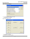
5 ispclock5400d evaluation board lattice semiconductor user’s guide 2. Set dip switches sw1 3 and 4 on and all other switches off. The blue lock led lights to indicate the on-chip pll is stable and locked to a reference clock. 3. Start pac-designer. 4. Choose file > open… the open dialog appears. 5....
Page 6
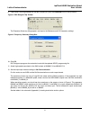
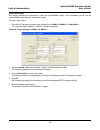
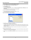
6 ispclock5400d evaluation board lattice semiconductor user’s guide 9. If the board is not programmed with the demo project yet, press the download icon on the top toolbar. Figure 4. Pac-designer top toolbar the frequency summary dialog appears and reports the reference and vco frequency settings. F...
Page 7
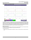
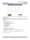
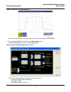
7 ispclock5400d evaluation board lattice semiconductor user’s guide figure 6. Scope plot - four differential outputs note: for user-designed boards and other applications, refer to the data sheet configurations and the schematics of appendix a. The schematic shows different resistor combinations for...
Page 8
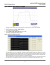
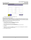
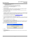
8 ispclock5400d evaluation board lattice semiconductor user’s guide figure 7. Scope plot - bank 0 and bank 2 overlapped note that a small inherent skew of the outputs plus any set-up delay in cables is about 50-80ps. 2. In pac-designer choose tools > design utilities… the design utilities dialog app...
Page 9
9 ispclock5400d evaluation board lattice semiconductor user’s guide 4. Position the mouse over the rising edge of the bank2 time waveform. The cursor will changes to a double-arrow icon to indicate a waveform edit. 5. Click and hold the bank 2 time waveform, then drag it three units to the right. Th...
Page 10
10 ispclock5400d evaluation board lattice semiconductor user’s guide invert clock output this section describes the procedure to invert the ispclock5406d output. In this procedure you will use the ispclock5406d invert feature to invert bank2 output. To invert a clock output: 1. From the pac-designer...
Page 11
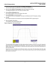
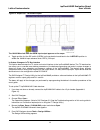
11 ispclock5400d evaluation board lattice semiconductor user’s guide figure 11. Scope plot - inverted output bank 6. Repeat steps 1-4 to adjust the output bank to not invert the output (inverted = no) and reprogram the device. Modify clock phase skew this section describes the procedure to modify ph...
Page 12
12 ispclock5400d evaluation board lattice semiconductor user’s guide figure 12. Scope plot - phase skew adjustment the waveform shows the bank_2 output advanced 1.24 ns. Modify the reference clock source input the evaluation board provides both 100 mhz (refa) and 156.25 mhz (refb) reference clock so...
Page 13
13 ispclock5400d evaluation board lattice semiconductor user’s guide figure 13. Scope plot - 156.25 mhz output the 156.25 mhz clock from the refb input output appears on the scope. 6. Toggle position 3 of the dip switch (user3) on the evaluation board back to the 1=ref-sel position to enable the 100...
Page 14
14 ispclock5400d evaluation board lattice semiconductor user’s guide figure 14. Design utilities dialog box 6. Select ispclock_5406_i2c_utility.Exe and click ok. The ispclock5406d i 2 c utility appears. Figure 15. Ispclock5406d i 2 c utility 7. Choose options > i2c interface… the cable and i/o port ...
Page 15
15 ispclock5400d evaluation board lattice semiconductor user’s guide 8. Click the change… button until the uses pc usb port title appears. 9. Disable the bypass hardware checking (demo mode) option. 10. Click the settings… button. The usb settings dialog appears. 11. From the select usb port name… s...
Page 16
16 ispclock5400d evaluation board lattice semiconductor user’s guide figure 17. Scope plot - skew measurement note a small inherent skew of the outputs plus any set-up delay in cables is about 50-80ps. 3. From the ispclock5406d i 2 c utility click the output group 1 button. The ispclock5406d output ...
Page 17
17 ispclock5400d evaluation board lattice semiconductor user’s guide - ref select, reference a or b mux control - phase–skew value, 16 values - output delay mode for zero-delay mode or fob, fan-out buffer mode 4. Double-click the bank 2 output block (0x0, 8 tud, 0=disable) of the schematic. The outp...
Page 18
18 ispclock5400d evaluation board lattice semiconductor user’s guide figure 20. Ispclock5406d soft reset dialog - soft reset released state 4. Click ok. Note the scope display changes to reflect the time-skewed waveform pattern produced earlier. I 2 c commands will be retained and reapplied after so...
Page 19
19 ispclock5400d evaluation board lattice semiconductor user’s guide 5. Specify ref frequency: 100 then click the internal feedback, modify... Button. The external feedback setting dialog appears. 6. Select internal feedback, select feedback taken from v-divider 8, and click ok. 7. From the pll core...
Page 20
20 ispclock5400d evaluation board lattice semiconductor user’s guide set up the evaluation board for a phase jitter measurement: 1. Set the evaluation board dip switches to enable 3.3v vcco. 2. Enable the refa oscillator input. 3. Disable the refb oscillator input. 4. Set the ref_sel switch to 0. 5....
Page 21
21 ispclock5400d evaluation board lattice semiconductor user’s guide 7. Click the browse… button. The save as dialog appears. 8. Browse to the destination folder, specify a file name, and click save. 9. Click ok. After a few moments the jedec programming file is output. 10. See the programming with ...
Page 22
22 ispclock5400d evaluation board lattice semiconductor user’s guide figure 21. Change programming cable interface dialog box 4. From the programming cable interface list, select uses pc usb and click ok. The cable and i/o port setup dialog appears. Figure 22. Cable and i/o port setup dialog box 5. ...
Page 23
23 ispclock5400d evaluation board lattice semiconductor user’s guide figure 23. Usb settings dialog box 6. Enable connect at startup and click ok. An information dialog appears. After altering the usb setting within these dialog boxes, pac-designer must be restarted to load the port drivers for the ...
Page 24
24 ispclock5400d evaluation board lattice semiconductor user’s guide figure 25. Frequency summary dialog box 4. Click ok. Pac-designer reprograms the evaluation board with the updated jedec programming file. Ispclock5400d evaluation board this section describes the features of the ispclock5400d eval...
Page 25
25 ispclock5400d evaluation board lattice semiconductor user’s guide the ispclock5406d can also be driven from an external differential clock source by moving the zero-ohm resistor from the r35 location to the r37 location and connecting the clocks to both refb_n and refb_p inputs (j1 and j2). When ...
Page 26
26 ispclock5400d evaluation board lattice semiconductor user’s guide figure 27. Bank 0 mlvds with on-board termination ispclock5406d standard evaluation board r16 r17 0 0 r23 33 r24 33 r25 22 r26 22 r28 0.1uf r29 0.1uf r30 34 r31 34 bank_0p j3 j4 bank_0n 50 5pf 50 5pf 50 ohms / 64.3 mm m c 1 9 / s m...
Page 27
27 ispclock5400d evaluation board lattice semiconductor user’s guide figure 29. Bank 0 sstl15/sstl18 with on board termination ispclock r16 r17 20 20 r23 71.5 r24 71.5 r25 45.3 r26 45.3 r28 r29 r30 0 r31 0 bank_0p j3 j4 bank_0n scope 50 5pf 50 5pf 50 ohms / 64.3 mm 50 ohms / 64.3 mm 50 ohms / 91 cm ...
Page 28
28 ispclock5400d evaluation board lattice semiconductor user’s guide hcsl hcsl termination involves a bias network to ground at the driver and no termination at the end of the t-line. Figure 32 shows the drivers biased through series resistors r16 and r17 (value of 33 ohms) combined with resis- tors...
Page 29
29 ispclock5400d evaluation board lattice semiconductor user’s guide ispclock_5400_i2c_outgroup_sch.Emf ispclock_5400_i2c_pll_sch.Emf 5. Rerun the ispclock5406d i 2 c utility. Environmental requirements the evaluation board must be stored between -40°c and 100°c. The recommended operating temperatur...
Page 30
30 ispclock5400d evaluation board lattice semiconductor user’s guide glossary i 2 c: inter-integrated circuit. Led: light-emitting diode. Pcb: printed circuit board. Rohs: restriction of hazardous substances directive. Pll: phase locked loop. References the following documentation is recommended for...
Page 31
31 ispclock5400d evaluation board lattice semiconductor user’s guide technical support assistance hotline: 1-800-lattice (north america) +1-503-268-8001 (outside north america) e-mail: techsupport@latticesemi.Com internet: www.Latticesemi.Com revision history date version change summary december 200...
Page 32
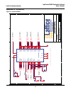
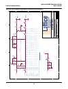
32 ispclock5400d evaluation board lattice semiconductor user’s guide appendix a. Schematic figure 33. Ispclock5406d 5 5 4 4 3 3 2 2 1 1 d d c c b b a a vcc tdo tdi tms tck bank_0n bank_0p bank_2n bank_2p bank_3n bank_3p bank_5n bank_5p refa_n refa_p refb_n refb_p scl sda vcco_0 vcco_2 vcco_3 vcco_5 ...
Page 33
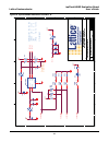
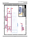
33 ispclock5400d evaluation board lattice semiconductor user’s guide figure 34. Ispclock5406d reference oscillator “a” 5 5 4 4 3 3 2 2 1 1 d d c c b b a a vcc vcc vcc vcc vcc vcc refa_n refa_p refa_en vcca refb_en user3 user0 date: size schematic rev of sheet title lattice semiconductor applications...
Page 34
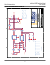
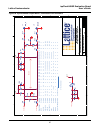
34 ispclock5400d evaluation board lattice semiconductor user’s guide figure 35. Ispclock5406d reference oscillator “b” 5 5 4 4 3 3 2 2 1 1 d d c c b b a a vcc vcc vcc refb_n refb_p refb_en date: size schematic rev of sheet title lattice semiconductor applications email: techsupport@latticesemi.Com p...
Page 35
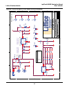
35 ispclock5400d evaluation board lattice semiconductor user’s guide figure 36. Ispclock5406d output bank 0 termination and connectors 5 5 4 4 3 3 2 2 1 1 d d c c b b a a vcco vcco vcco bank_0p bank_0n vcco_0 date: size schematic rev of sheet title lattice semiconductor applications email: techsuppo...
Page 36
36 ispclock5400d evaluation board lattice semiconductor user’s guide figure 37. Ispclock5406d output bank 2 termination and connectors 5 5 4 4 3 3 2 2 1 1 d d c c b b a a vcco vcco vcco bank_2p bank_2n vcco_2 date: size schematic rev of sheet title lattice semiconductor applications email: techsuppo...
Page 37
37 ispclock5400d evaluation board lattice semiconductor user’s guide figure 38. Ispclock5406d output bank 3 termination and connectors 5 5 4 4 3 3 2 2 1 1 d d c c b b a a vcco vcco vcco bank_3p bank_3n vcco_3 date: size schematic rev of sheet title lattice semiconductor applications email: techsuppo...
Page 38
38 ispclock5400d evaluation board lattice semiconductor user’s guide figure 39. Ispclock5406d output bank 5 termination and connectors 5 5 4 4 3 3 2 2 1 1 d d c c b b a a vcco vcco vcco bank_5p bank_5n vcco_5 date: size schematic rev of sheet title lattice semiconductor applications email: techsuppo...
Page 39
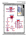
39 ispclock5400d evaluation board lattice semiconductor user’s guide figure 40. +12v to +5v input 3.3v vcc output and vcco adjustable 5 5 4 4 3 3 2 2 1 1 d d c c b b a a +7.5v vcc 0 vcco date: size schematic rev of sheet title lattice semiconductor applications email: techsupport@latticesemi.Com pho...
Page 40
40 ispclock5400d evaluation board lattice semiconductor user’s guide figure 41. Test, jtag and i 2 c interface and connectors 5 5 4 4 3 3 2 2 1 1 d d c c b b a a sdin scl sda vcc vcc vcc vcc vcc vcc vcc vcc vcco tdo tdi tms tck sda scl resetb refa_en refb_en user0 user3 refb_vtt fbk_vtt date: size s...
Page 41
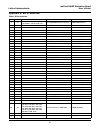
41 ispclock5400d evaluation board lattice semiconductor user’s guide appendix b. Bill of materials table 3. Bill of materials item quantity reference part part number 1 24 c13, c12, c15, c18, c21, c24, c26, c30-31, c35-45, c46, c47 0.1uf smd 0805 ceramic capacitor c0805c104k5ractu 2 2 c4, c7 1.0 uf ...
Page 42
42 ispclock5400d evaluation board lattice semiconductor user’s guide 39 2 q1, q2 npn trans. Sot-23 mmbt2369a 40 1 q3 npn trans. Sot-223 fzt649ta 41 1 u1 isppac-clk5406d 42 1 u2 3.3v fixed regulator smd 8soic tps77733d 43 1 u3 adj ldo regulator smd 8soic tps77701d 44 1 u4 74lvc3g34 triple buffer 8-ss...


