Lattice Semiconductor ispLever Core Multi-Channel DMA Controller User Manual
Summary of ispLever Core Multi-Channel DMA Controller
Page 1
February 2006 ipug11_04.0 multi-channel dma controller user’s guide isp lever core core tm.
Page 2
Lattice semiconductor multi-channel dma controller user’s guide 2 introduction the multi-channel direct memory access (mcdma) controller is designed to improve microprocessor system per- formance by allowing external devices to transfer information directly from the system memory and vice versa. Mem...
Page 3
Lattice semiconductor multi-channel dma controller user’s guide 3 • software dma requests.
Page 4
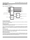
Lattice semiconductor multi-channel dma controller user’s guide 4 block diagram figure 1 shows the block diagram of this core. Figure 1. Block diagram of mcdma core functional description the mcdma contains three basic blocks of control logic: cpu interface (data and control blocks), the dma state m...
Page 5
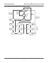
Lattice semiconductor multi-channel dma controller user’s guide 5 • illegal i/o to memory transfer mode bits • compressed timing mode fsm operation when a software or hardware request is received and is found to be valid (having passed the polarity, mask and mode checks), the dma fsm in si (idle) st...
Page 6
Lattice semiconductor multi-channel dma controller user’s guide 6 figure 2. Mcdma finite state machine for 8237 and non-8237 modes request dropped illegal mode illegal i/o mode (8237 only) last_tran/ single_tran termination last_tran/ single_tran termination write phase read phase another t ransfer ...
Page 7
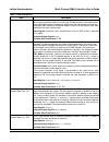
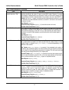
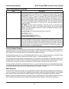
Lattice semiconductor multi-channel dma controller user’s guide 7 table 2. State descriptions state description idle state - si upon reset, the state machine enters the idle state, si. The cpu can program the core’s internal registers while it is in this state. The device stays in this state until a...
Page 8
Lattice semiconductor multi-channel dma controller user’s guide 8 memory-to-memory read transfer state three - s13 this is the third state of the memory-to-memory transfer. The state machine sam- ples the ready signal and stays in this state as long as it is asserted. The machine transitions to stat...
Page 9
Lattice semiconductor multi-channel dma controller user’s guide 9 memory-to-memory write transfer state four - s24 this is the eighth and final stage of the memory-to-memory transfer. The state machine de-asserts the memw_n signal. In the 8237 mode, channel 1’s current word register is decremented. ...
Page 10
Lattice semiconductor multi-channel dma controller user’s guide 10 priority request encoder this block prioritizes the dma request and asserts the dack signal for the winning request. In the 8237 mode, the arbitrating scheme is user programmable and available in either a fixed priority or rotating p...
Page 11
Lattice semiconductor multi-channel dma controller user’s guide 11 the functionality of the core in the non-8237 mode is very similar to that of the 8237 mode. However, the two modes have totally different sets of programmable control registers. This increases the programmability features in the non...
Page 12
Lattice semiconductor multi-channel dma controller user’s guide 12 • demand transfer mode: in demand transfer mode, the device is programmed to continue making transfers until a terminal count or external eopin_n is encountered or until dreq goes inactive. Thus, transfers continue until the i/o devi...
Page 13
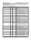
Lattice semiconductor multi-channel dma controller user’s guide 13 signal descriptions table shows the input and output ports of the mcdma core that apply for both 8237 and non-8237 modes. Table 4. Signal definitions of the mcdma controller port name type active state description clk input rising ed...
Page 14
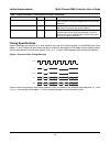
Lattice semiconductor multi-channel dma controller user’s guide 14 timing specifications figure 3 illustrates the waveform for a write operation into one of the internal registers in the mcdma core. Clock edges 1, 2 and 3 indicate the point where the data is written into the registers. Clock edges 2...
Page 15
Lattice semiconductor multi-channel dma controller user’s guide 15 figure 4. Processor read timing waveform clock cs_n iorin_n ain 1 2 3 dbout.
Page 16
Lattice semiconductor multi-channel dma controller user’s guide 16 figure 5 shows the timing waveform for two words dma transfer. Figure 5. Two word dma transfer timing waveform clock dreq hreq si s0 s0 s1 s2 s3 s4 aen aout dack iorout_n/memr_n s2 s3 s4 valid address note 1. Iowout_n/memw_n hlda val...
Page 17
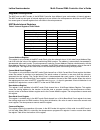
Lattice semiconductor multi-channel dma controller user’s guide 17 register descriptions the 8237 and non-8237 modes of the mcdma controller have different types and number of internal registers. The 8237 mode has ten types of internal registers that are visible to the microprocessor while the non-8...
Page 18
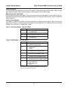
Lattice semiconductor multi-channel dma controller user’s guide 18 mode register each channel has a 6-bit wide register. During a write operation by the microprocessor when mcdma is in idle state, the least two significant bits (bit 0 and 1) of the data bus determine which channel mode register is b...
Page 19
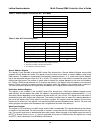
Lattice semiconductor multi-channel dma controller user’s guide 19 table 7. Mode register - 8237 mode table 8. Mask register: access all bits - 8237 mode table 9. Mask register: access one bit - 8237 mode table 10. Request register: access one bit - 8237 mode bit description 1:0 00 channel 0 select ...
Page 20
Lattice semiconductor multi-channel dma controller user’s guide 20 table 11. Status register: access one bit – 8237 mode table 12. Non-8237 internal registers source address register this register is only available in the non-8237 mode. Each channel has a source address register whose width matches ...
Page 21
Lattice semiconductor multi-channel dma controller user’s guide 21 command register this register controls the operation of the core. This register is 4 bits wide in the non-8237 mode. A reset or master clear clears the register. Table 13 lists the functions of this register for the non-8237 mode. M...
Page 22
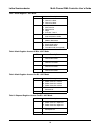
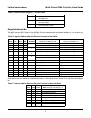
Lattice semiconductor multi-channel dma controller user’s guide 22 table 15. Channel control register – non-8237 mode register address map the 8237 and non-8237 modes of the mcdma controller decode and use different numbers of ain bit input sig- nals. The ain signal is used for mapping the register ...
Page 23
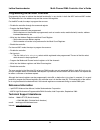
Lattice semiconductor multi-channel dma controller user’s guide 23 programming the mcdma controller programming the core to achieve the desired functionality is very similar in both the 8237 and non-8237 modes. The differences lie in the address map and the name of the registers for the 8237 mode, t...
Page 24
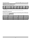
Lattice semiconductor multi-channel dma controller user’s guide 24 appendix for orca ® series 4 fpgas table 18. Performance and resource utilization 1 supplied netlist configurations the ordering part number (opn) for all configurations of this core in orca series 4 devices is dma-mc-o4-n2. Table 19...
Page 25
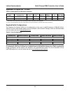
Lattice semiconductor multi-channel dma controller user’s guide 25 appendix for ispxpga ® fpgas table 20. Performance and resource utilization 1 supplied netlist configurations the ordering part number (opn) for all configurations of this core in ispxpga devices is dma-mc-xp-n2. Table 21 lists the l...
Page 26
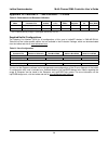
Lattice semiconductor multi-channel dma controller user’s guide 26 appendix for latticeecp™ and latticeec™ fpgas table 22. Performance and resource utilization 1 supplied netlist configurations the ordering part number (opn) for all configurations of this core in latticeec devices is dma-mc-e2-n3. T...
Page 27
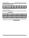
Lattice semiconductor multi-channel dma controller user’s guide 27 appendix for latticexp™ fpgas table 24. Performance and resource utilization 1 supplied netlist configurations the ordering part number (opn) for all configurations of this core in latticexp devices is dma-mc-xm-n3. Table 25 lists th...
Page 28
Lattice semiconductor multi-channel dma controller user’s guide 28 appendix for latticesc™ fpgas table 26. Performance and resource utilization 1 supplied netlist configurations the ordering part number (opn) for all configurations of this core in latticesc devices is dma-mc-sc-n3. Table 27 lists th...
Page 29: Mouser Electronics
Mouser electronics authorized distributor click to view pricing, inventory, delivery & lifecycle information: lattice : dma-mc-e2-n3 dma-mc-o4-n2 dma-mc-xm-n3 dma-mc-xp-n2 dma-mc-sc-n3.


