- DL manuals
- Lattice Semiconductor
- Motherboard
- L-ASC10
- User Manual
Lattice Semiconductor L-ASC10 User Manual
Summary of L-ASC10
Page 1
Asc breakout board user guide eb92 version 1.0, july 2015.
Page 2
2 asc breakout board introduction thank you for choosing the lattice semiconductor asc breakout board. This guide describes how to begin using the l-asc10 (asc) breakout board, an easy-to-use platform for evaluat- ing and designing with the asc programmable hardware management expander. This board i...
Page 3
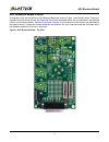
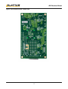
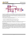
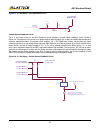
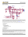
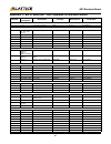
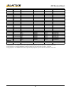
3 asc breakout board asc breakout board photos photographs of the top and bottom of asc breakout board are shown in figure 1 and figure 2 below. These pho- tographs show the board with the hot swap and trim circuits populated (which are not populated in the released version of the breakout board). S...
Page 4
4 asc breakout board figure 2. Asc breakout board - bottom view.
Page 5
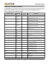
5 asc breakout board board hardware features the asc breakout board is provided with a limited set of circuits populated. The circuits populated on the breakout board are described first. The breakout board also includes connections and footprints for evaluating the trimming and hot swap functions o...
Page 6
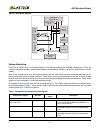
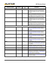
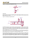
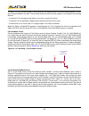
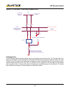
6 asc breakout board figure 3. Asc block diagram voltage monitoring there are 10 vmon inputs to the analog section of the device (including the himonn_hvmon pin). These are routed to slide potentiometers, board power supplies (not populated), and the on-board hot swap circuits (not pop- ulated). Mos...
Page 7
7 asc breakout board components not populated on breakout board series resistors r23 1 , r32 1 3 270 Ω resistor allows the user to safely drive vmon1 and vmon2 test points with an off-board voltage source. (only needed when dcdc1 and dcdc2 are populated.) ground sense resistors r24 1 , r33 1 3 100 Ω...
Page 8
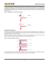
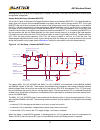
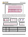
8 asc breakout board the two potentiometers (r50 and r52) are tied to vmon7 and vmon8 these can be used to simulate a fault or trip a comparator (see figure 4). The slide potentiometers provide a voltage in the range of 0 v to 3.3 v depending on their position. R51 and r53 are 1 k Ω series resistors...
Page 9
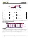
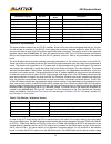
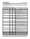
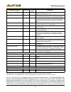
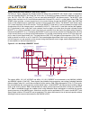
9 asc breakout board figure 6. Temperature monitor connections the temperature monitor components and signals are summarized in table 2 below. Table 2. Temperature monitor components and signals led outputs the asc breakout board has 9 leds tied to the asc open-drain outputs. The leds are pulled up ...
Page 10
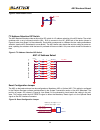
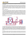
10 asc breakout board figure 8. Push-button circuit i 2 c address selection dip switch the asc breakout board provides an 8-position dip switch for i 2 c address selection of the asc device. The switch combines with a set of on-board resistors (r9 – r15) to connect to the i2c_addr pin of the device ...
Page 11
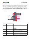
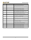
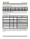
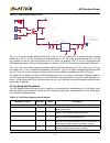
11 asc breakout board asc interface connector the asc interface connector (shown in figure 11 from schematic sheet 2) is used to connect the asc breakout board to the main fpga board. The connector has been designed to pair with other available lattice evaluation boards, including the platform manag...
Page 12
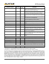
12 asc breakout board 9 +3.3v asc supply voltage. Provided by fpga board or 12 v power supply (power supply not populated on breakout board). 10 +11.3v voltage rail generated from diode or of +12v_sw and +5_sw input supplies. Fpga main board may use as input to 12 v dc-dc convert- ers. 11 +12v_hs 12...
Page 13
13 asc breakout board closed loop trimming (not populated) the asc provides four closed loop trim (clt) cells which are used to accurately trim and margin power supplies. The asc breakout board provides four dc-dc converter and trimming circuit footprints on the breakout board. Table 4 lists the com...
Page 14
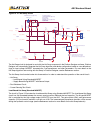
14 asc breakout board overview of trim and margin the board provides footprints for four dc-dc modules. Since all four are similarly designed and laid out, this sec- tion will provide an overview of the dc-dc circuit rather than provide a separate section for each dc-dc. Foot- prints are provided fo...
Page 15
15 asc breakout board source to be applied to the vmon test point directly. If the voltage source is fairly weak, the vmon series resistor can be removed. Each of the dc-dc supplies has a load resistor connected to the output. The load resistor is not required in cus- tomer designs as the supply is ...
Page 16
16 asc breakout board table 6 shows a summary of the input voltage, output voltage, and control signal behavior for each of the four dc- dc converters. The +12v_hs and +5v_hs rails which are used to power the dc-dc converters can be provided by either the hot swap circuits or the asc interface board...
Page 17
17 asc breakout board figure 13. Board power supply circuit the +12 v connects through schottky diode d16 to the +11.3 v rail, while the +5 v connects through schottky diode d18 to the +11.3 v rail. Through this configuration, the +11.3 v rail will be sourced by either the +12v_sw rail (if present) ...
Page 18
18 asc breakout board the 5 v hot swap circuit is designed to support two separate implementations. The standard mosfet implemen- tation uses a standard power mosfet (q6) and a 5 m Ω sense resistor (r60). The mosfet with sense output implementation uses a power mosfet with current sense output (q5) ...
Page 19
19 asc breakout board figure 14. 5 v hot swap circuit the hot swap circuit is designed to work with the hot swap component in the platform designer software. Platform designer will automatically generate the hot swap algorithm and device configuration based on user defined set- tings for input volta...
Page 20
20 asc breakout board figure 15. 5 v hot swap - load-based, standard mosfet the signals 5v_hs_current_p and 5v_hs_current_n are connected to the imon1p and imon1n signals of the asc. The sensing resistor r60 is connected through the zero Ω isolation resistors (r58, 59) to the asc using kelvin connec...
Page 21
21 asc breakout board figure 16. 5 v hot swap - supply based, sensefet the signals 5v_hs_current_p and 5v_hs_current_n are connected to the imon1p and imon1n signals of the asc. In the mosfet with sense output variation, r57 is used as the sensing resistor. R57 is tied between the sense current outp...
Page 22
22 asc breakout board figure 17. 5 v hot swap – fast shutdown circuit current sense feedback circuit the 5 v hot swap circuit on the asc breakout board includes a current sense feedback circuit, shown in figure 18. The purpose of this circuit is for demonstration and evaluation only, it does not nee...
Page 23
23 asc breakout board 12 v hot swap (not populated) the asc breakout board provides a set of footprints and connections for implementing a 12 v hot swap circuit using the asc’s built in hardware. Table 9 lists the key elements associated with 12 v hot swap operation on the asc breakout board. Table ...
Page 24
24 asc breakout board the 12 v hot swap circuit is designed to support two separate implementations. The standard mosfet imple- mentation uses standard power mosfets (q9 and q10) and a 10 m Ω sense resistor (r73). The mosfet with sense output implementation uses a power mosfet with current sense out...
Page 25
25 asc breakout board shown in figure 19 below. Figure 19. 12 v hs circuit the hot swap circuit is designed to work with the hot swap component in the platform designer software. Platform designer will automatically generate the hot swap algorithm and device configuration based on user defined set- ...
Page 26
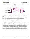
26 asc breakout board figure 20. 12 v hot swap - input voltage monitor circuit charge pump the 12 v hot swap circuit requires a charge pump to boost the gate voltage to around 20 v to fully turn on the mosfet to conduct 12 v. The circuit shown in figure 21 is used to implement this external charge p...
Page 27
27 asc breakout board discharge path for c19 when the charge pump is disabled. The pump_v test point can be used for monitoring the charge pump voltage level. Supply-based hot swap (standard mosfet) the circuit in figure 22 illustrates the supply-based hot swap using standard mosfets. The supply-bas...
Page 28
28 asc breakout board supply-based hot swap (mosfet with sense output) the circuit in figure illustrates the supply-based hot swap using a mosfet with sense output. (components from the standard mosfet hot swap are shown also to illustrate the shared connections between the two cir- cuits. Q9, r71, ...
Page 29
29 asc breakout board the mon_12v_hs_voltage signal is also used by the hot swap function to monitor the load capacitor c15 volt- age using the hvmon of the asc. The hot swap function monitors the load capacitor c15 voltage for the following reasons: • to see that c15 is charging up and there is not...
Page 30
30 asc breakout board figure 25. 12 v hot swap - current sense feedback circuit prototype area the asc breakout board provides multiple areas for prototyping circuits with the asc. The through hole proto- type area (see sheet 10 of the schematic) is accessible from both the top and bottom side of th...
Page 31
31 asc breakout board figure 26. Through hole prototype area the asc breakout board also provides a surface-mount prototyping area on the bottom side of the board. The sur- face mount area is near the through hole prototyping area and provides a set of common footprints for resistors, capacitors, di...
Page 32
32 asc breakout board mechanical specifications dimensions: 6 in. [l] x 3.5 in. [w] x 1 in. [h] environmental specifications the breakout board must be stored between -40°c and 100°c. The recommended operating temperature is between 0°c and 55°c. Electrical specifications • 12 v input +/- 15% (input...
Page 33
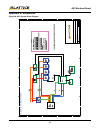
33 asc breakout board appendix a. Schematics figure 28. Asc system block diagram 5 5 4 4 3 3 2 2 1 1 d d c c b b a a content s asc sy stem block diagram da te : si z e sc h e m a ti c re v of sheet ti tl e lat ti c e s e m icond u ct or a p pl ic at ions e m ai l: t e chs u ppor t@ lat ti c e s e m ...
Page 34
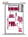
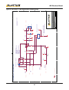
34 asc breakout board figure 29. Analog sense and control 5 5 4 4 3 3 2 2 1 1 d d c c b b a a asc test points a n alog s e nse and control mandatory asc jumper 2 to 3 optional asc jumper 1 to 2 a s c i 2 c a d dr ess sel e ct 1 3 2 4 5 7 6 a s c i n te rf ace connect o r 0 asc_ w dat asc_ rdat asc_ ...
Page 35
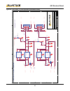
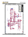
35 asc breakout board figure 30. Trims dcdc 1-2 (not populated on breakout board) 5 5 4 4 3 3 2 2 1 1 d d c c b b a a gp io9 3. 3v @ 3a 5v @ 3a gp io8 tr im 1 tr im 2 vm o n 2 vm o n 1 trims dcdc 1-2 ( n ot p o p u lated) 5v @ 2a 3. 3v @ 2a sip n o te : components not popula te d o n breakout b o a ...
Page 36
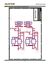
36 asc breakout board figure 31. Trims dcdc 3-4 (not populated on breakout board) 5 5 4 4 3 3 2 2 1 1 d d c c b b a a gp io4 2. 5v @ 3a trims dcdc 3-4 ( n ot p o p u lated) tr im 3 vm o n 3 1. 2v @ 3a gp io5 vm o n 4 tr im 4 1. 2v @ 2a 2. 5v @ 2a sip n o te: compone nts not popula te d o n breakout ...
Page 37
37 asc breakout board figure 32. Inputs: temperature sensors, trim pots & switches 5 5 4 4 3 3 2 2 1 1 d d c c b b a a temperature sensor 1 temperature sensor 2 inp u ts: tem p erat u re sensors, trim pots & s w itches vm o n 7 vm o n 8 +3. 3 v +3. 3 v po t1 sh e e t [ 2 ] po t2 sh e e t [ 2 ] tem p...
Page 38
38 asc breakout board figure 33. Hot swap, 5 v (not populated on breakout board) 5 5 4 4 3 3 2 2 1 1 d d c c b b a a hot s w ap, 5 v ( n ot p o p u lated) imon vm o n 6 hvo u t 2 popul a ti on o p ti ons: st andar d m o sfet ( o pt ion a ): q6 , c 2 2 , r 6 1 , r6 0 , r5 8 , r5 9 m o sfet w / sense ...
Page 39
39 asc breakout board figure 34. Hot swap, 12 v (not populated on breakout board) 5 5 4 4 3 3 2 2 1 1 d d c c b b a a hot s w ap, 12 v ( n ot p o p u lated) hi m o n as c i n t c onnect o r vm o n 9 hvo u t 1 sense x 600 i_12v_h s - 1v per 1a sensed popul a ti on o p ti ons: st andar d m o sfet ( o ...
Page 40
40 asc breakout board figure 35. Leds 5 5 4 4 3 3 2 2 1 1 d d c c b b a a le ds le d 2 le d 3 le d 4 le d 5 le d 6 le d 8 le d 9 le d 1 0 le d 1 le d [1: 10] s h e e t [2 ,3 ,4 ,5 ] +3. 3 v s h e e t [2 ,3 ,4 ,5 ,6 ,7 ,9 ,1 0 ] da te : si z e sc h e m a ti c re v of s h eet ti tl e lat ti ce s e m i...
Page 41
41 asc breakout board figure 36. Board power (not populated on breakout board) 5 5 4 4 3 3 2 2 1 1 d d c c b b a a populate jumper to provide 3.3v power from asc eval board 3.3v 1a 12v to 4.8v input range b o ard p o w er ( n ot p o p u lated) n o te: compone nts not popula te d o n breakout b o a r...
Page 42
42 asc breakout board figure 37. Prototype and mounting holes 5 5 4 4 3 3 2 2 1 1 d d c c b b a a p rototy pe & m o u nting holes so t -23 packa g e pr ot ot y p e a rea sm d so t -223 pr ot ot y p e a rea sm d 2512 r esi st or packa g e pr ot ot y p e a rea s o ic -8 p a c k a g e pr ot ot y p e a ...
Page 43
43 asc breakout board figure 38. Mechanical drawing 5 5 4 4 3 3 2 2 1 1 d d c c b b a a m e chanical dra w ing da te : si z e sc h e m a ti c re v of s h eet ti tl e lat ti c e s e m icond u c to r a p p lic a tio n s e m a il: te c h s u p p o rt@ l a ttic e s e m i.C o m b o ar d r e v pr o je c t...
Page 44
44 asc breakout board appendix b. Bill of materials – populated on breakout board quantity reference designator description package manufacturer part number ics 1 u1 asc device tqfn_48 lattice semiconductor l-asc10-1sg48i capacitors 2 c1, c2 0.1uf 16 v 10% ceramic x7r smd 0603 murata grm188r71c104ka...
Page 45
45 asc breakout board appendix c. Bill of materials – not populated on breakout board quantity reference designator description package manufacturer part number ics 2 u2, u3 current sense amplifier sot23 diodes inc zxct1009fta capacitors 8 c18, c20 1 , c21 1 , c22 3 , c23 4 , c26 2 , c31, c32 0.1 uf...
Page 46
46 asc breakout board 1 r39, r86, r88, r90, r92 470 Ω resistor smd 0603 panasonic erj-3geyj471v 5 r43 20.0 k Ω resistor smd 0603 panasonic erj-3ekf2002v 1 r44 39.0 k Ω resistor smd 0603 panasonic erj-3ekf3902v 1 r47 330 Ω resistor smd 0603 panasonic erj-3geyj331v 2 r54 4 ,r67 2 2.2 k smd 0603 panaso...
Page 47
47 asc breakout board appendix d. Known issues the populated components on the breakout board work as specified without issue. There is an issue related to the footprints and connections in the 12 v hot swap – charge pump section of the board. The footprint for q17 contains an error in the connectio...
Page 48
48 asc breakout board figure 41. Q17 - orientation for corrected connection.
Page 49: Mouser Electronics
Mouser electronics authorized distributor click to view pricing, inventory, delivery & lifecycle information: lattice : lptm-asc-b-evn.

