Lattice Semiconductor LatticeECP2M SERDES User Manual
Summary of LatticeECP2M SERDES
Page 1
May 2010 revision: eb25_01.7 latticeecp2m™ serdes evaluation board user’s guide.
Page 2
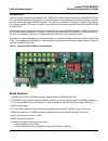
2 latticeecp2m serdes lattice semiconductor evaluation board user’s guide introduction this user’s guide describes the latticeecp2m™ serdes evaluation board featuring the latticeecp2m fpga. This stand-alone evaluation pcb provides a functional platform for development and rapid prototyping of applic...
Page 3
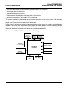
3 latticeecp2m serdes lattice semiconductor evaluation board user’s guide • orcastra demonstration software interface via standard ispvm jtag connection • various high-speed layout structures • user-defined input and output points • sma connectors included (10) for high-speed clock or data interfaci...
Page 4
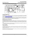
4 latticeecp2m serdes lattice semiconductor evaluation board user’s guide figure 3. Latticeecp2m serdes evaluation board, top view latticeecp2m device this board features a latticeecp2m fpga with a 1.2v core supply. It can accommodate all pin compatible latticeecp2m devices in the 672-ball fpbga (1m...
Page 5
5 latticeecp2m serdes lattice semiconductor evaluation board user’s guide table 1. Board power supply fuses (see appendix a, figure 4) f1 1.2v core fuse f2 1.5v fuse f3 3.3v fuse f4 1.2v fuse f5 2.5v fuse f6 1.8v fuse table 2. Board power supply indicators (see appendix a, figure 4) d1 2.5v source g...
Page 6
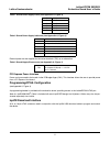
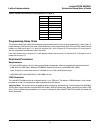
6 latticeecp2m serdes lattice semiconductor evaluation board user’s guide table 4. Ispvm jtag connector (see appendix a, figure 2) pin 1 vcc pin 2 tdo pin 3 tdi pin 4 programn pin 5 nc pin 6 tms pin 7 gnd pin 8 tck pin 9 done pin 10 initn programming daisy chain this board includes two lattice semic...
Page 7
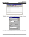
7 latticeecp2m serdes lattice semiconductor evaluation board user’s guide 1. Press the scan button located in the toolbar. The latticeecp2m device will automatically be detected. 2. Double-click the device to open the device information dialog. In the device information dialog, click the browse butt...
Page 8
8 latticeecp2m serdes lattice semiconductor evaluation board user’s guide configuration status indicators (see appendix a, figure 4) these leds indicate the status of configuration to the fpga. • d8 (red) illuminated – indicates that programming was aborted or reinitialized, driving the initn output...
Page 9
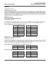
9 latticeecp2m serdes lattice semiconductor evaluation board user’s guide table 5. Sma clock input sma signal j35 u2 reference + input j36 u2 reference - input u2 is an ispclock5620a clock generator that allows designers to implement clock distribution networks supporting multiple, synchronized outp...
Page 10
10 latticeecp2m serdes lattice semiconductor evaluation board user’s guide serdes (see appendix a, figure 5) serdes reference clock the 50-ohm terminated sma connectors provide supply reference clocks directly to the latticeecp2m device from the ispclock management device. This device drives clocks ...
Page 11
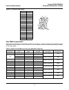
11 latticeecp2m serdes lattice semiconductor evaluation board user’s guide serdes sata channels (see appendix a, figure 5) connections are included to attach sata type cables to serdes channels for board-to-board or loopback pur- poses. The connectors are configured using the 7-pin sata specificatio...
Page 12
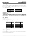
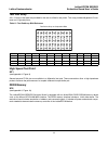
12 latticeecp2m serdes lattice semiconductor evaluation board user’s guide figure 4. 17-segment led display segment bga a b c d e f g h k m n p r s t u dp h2 j3 g1 h3 j7 h5 g5 g6 f3 j8 e1 j9 e3 f5 d3 f6 c2 a b c d g f e dp h t s r k m n u p test sma connections general-purpose fpga pins are availabl...
Page 13
13 latticeecp2m serdes lattice semiconductor evaluation board user’s guide test pad array a 5 x 12 array of test pads are provided for the user to utilize for test points. This array provides 48 general i/o con- tacts and 12 ground points. Table 13. Test pad array bga reference 1 2 3 4 5 6 7 8 9 10 ...
Page 14
14 latticeecp2m serdes lattice semiconductor evaluation board user’s guide ordering information description ordering part number china rohs environment-friendly use period (efup) latticeecp2m35 serdes evaluation board (non-rohs, obsolete) lfe2m35e-s-ev 10 latticeecp2m50 serdes evaluation board (non-...
Page 15
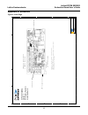
15 latticeecp2m serdes lattice semiconductor evaluation board user’s guide appendix a. Schematic figure 5. Cover page 5 5 4 4 3 3 2 2 1 1 d d c c b b a a title v e r t c ej or p e zi s t e e h s : et a d of ecp2m pci express card 1.0 cover page c 11 1 title v e r t c ej or p e zi s t e e h s : et a ...
Page 16
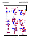
16 latticeecp2m serdes lattice semiconductor evaluation board user’s guide figure 6. Dc/dc conversion 5 5 4 4 3 3 2 2 1 1 d d c c b b a a 2_5_trim core_tri m 1_2_trim 3_3_trim 12_0v 2_5v 3_3v 12_0v vcc_core 1_5v 2_5v 12_0v 1_2v 1_8v 12_0v 12_0v vcc_core 3_3vin 12_0v 1_8v 1_5v 1_2v 3_3vin 3_3vin 12_0...
Page 17
17 latticeecp2m serdes lattice semiconductor evaluation board user’s guide figure 7. 5 5 4 4 3 3 2 2 1 1 d d c c b b a a vcc_core vddtx 1_2v vddp vddrx 1_8v vcc_core 2_5v vddrx vcc_core vddtx vddp 3_3v vddp vddtx vddrx 3_3v 2_5v 3_3v 1_8v 1_5v 1_2v vddib vddob 1_5v 1_2v vddib vddob 1_2v vcc_pll vcc_...
Page 18
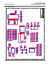
18 latticeecp2m serdes lattice semiconductor evaluation board user’s guide figure 8. 5 5 4 4 3 3 2 2 1 1 d d c c b b a a sflash_q_0 sflash_q_1 tck local_tdi local_tck tdi_buf local_tms local_tdo tck tdo_ec tdi_ec gsrn programn initn done done initn tms_buf sflash_q_0 flash_dis gsrn pro gr amn cfg2 c...
Page 19
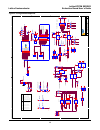
19 latticeecp2m serdes lattice semiconductor evaluation board user’s guide figure 9. Serdes 5 5 4 4 3 3 2 2 1 1 d d c c b b a a petp0 l_hdinp0 50 l_hdinn0 50 l_hdoutp0 50 l_hdoutn0 50 u_hdinn0 u_hdinn1 u_hdinp1 u_hdinp2 u_hdinn2 u_hdoutn0 u_hdoutn1 u_hdoutp1 u_hdoutn2 u_hdoutp2 u_hdoutp0 u_hdinp0 u_...
Page 20
20 latticeecp2m serdes lattice semiconductor evaluation board user’s guide figure 10. 5 5 4 4 3 3 2 2 1 1 d d c c b b a a ddr2_dq4 ddr2_dq12 ddr2_dq13 ddr2_dq15 ddr2_dq5 ddr2_dq6 ddr2_dq7 ddr2_dq8 ddr2_dq9 ddr2_dq0 ddr2_dq1 ddr2_dq2 ddr2_dq3 ddr2_dq11 ddr2_dq10 ddr2_dq14 dq10 dq11 dq12 dq13 dq14 dq8...
Page 21
21 latticeecp2m serdes lattice semiconductor evaluation board user’s guide figure 11. Ddr2 device/termination 5 5 4 4 3 3 2 2 1 1 d d c c b b a a ddr2_dqs0 ddr2_dq1 ddr2_dq4 ddr2_dq6 ddr2_dq2 ddr2_dq0 ddr2_dq5 ddr2_dq7 ddr2_dq3 ddr2_dq8 ddr2_dq[0:15] ddr2_dq9 ddr2_dq14 ddr2_dq13 ddr2_dq11 ddr2_dq10 ...
Page 22
22 latticeecp2m serdes lattice semiconductor evaluation board user’s guide figure 12. Clocks 5 5 4 4 3 3 2 2 1 1 d d c c b b a a osc_in_2 osc_in_4 osc_in_3 osc_in_1 oey ps0 refclk_ext_in_p oex refsel pll_bypass sgate goe ispclk_rst ps1 osc_p refclk_ext_in_n osc_n ispclk_lock u_refclk p refa_p refa_n...
Page 23
23 latticeecp2m serdes lattice semiconductor evaluation board user’s guide figure 13. 5 5 4 4 3 3 2 2 1 1 d d c c b b a a loop_n15 loop_p15 lvds_outn_0 lvds_inp_0 lvds_inn_0 lvds_inp_1 lvds_inn_1 lvds_inp_2 lvds_inn_2 lvds_inp_3 lvds_inn_3 lvds_outp_0 lvds_outp_1 lvds_outn_1 lvds_outp_2 lvds_outn_2 ...
Page 24
24 latticeecp2m serdes lattice semiconductor evaluation board user’s guide figure 14. Fpga test 5 5 4 4 3 3 2 2 1 1 d d c c b b a a red1 yellow1 green1 blue1 red2 yellow2 green2 blue2 switch5 switch6 switch7 switch8 switch3 switch2 switch4 switch1 green1 green2 red1 red2 blue1 blue2 yellow1 yellow2 ...
Page 25
25 latticeecp2m serdes lattice semiconductor evaluation board user’s guide figure 15. Vss/decoupling 5 5 4 4 3 3 2 2 1 1 d d c c b b a a vddob vddrx vddtx 3_3v vddp vcc_core 2_5v 2_5v 2_5v 2_5v 2_5v vddib 2_5v 1_8v 2_5v title v e r t c ej or p e zi s t e e h s : et a d of sc pci express card 1.0 vss...


