- DL manuals
- Lattice Semiconductor
- PCI Card
- LatticeECP3
- User Manual
Lattice Semiconductor LatticeECP3 User Manual
Summary of LatticeECP3
Page 1
August 2012 revision: eb43_01.2 latticeecp3 pci express solutions board – revision a user’s guide.
Page 2
2 latticeecp3 pci express solutions board – revision a user’s guide introduction as pci express applications have emerged, the latticeecp3™ fpga family has become a well-suited solution for many system designs. The features of the latticeecp3 pci express solutions board can assist engineers with rap...
Page 3
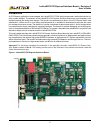
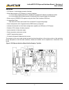
3 latticeecp3 pci express solutions board – revision a user’s guide features • pci express x1 and x4 edge connector interfaces • allows demonstration of pci express (x 1and x4) interfaces – x1 is form-factor compliant and will fit a standard pc-equipped pci express motherboard socket – x4 is non-com...
Page 4
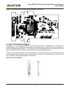
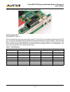
4 latticeecp3 pci express solutions board – revision a user’s guide figure 3. Pci express solutions board outline drawing, bottom side x1 and x4 pci express support pci express x1 and x4 is supported with the same pcb. This add-in pcb is designed to work in both types of motherboard slots. The pcb c...
Page 5
5 latticeecp3 pci express solutions board – revision a user’s guide latticeecp3 device this board features a latticeecp3 fpga with a 1.2v core supply. It can accommodate all pin compatible latticeecp3 devices in the 672-ball fpbga (1mm pitch) package. A complete description of this device can be fou...
Page 6
6 latticeecp3 pci express solutions board – revision a user’s guide pci express power interface power can be sourced to the board via the pcb edge-fingers (cn1 and cn2). This interface allows the user to pro- vide power from a pci express host board. Programming/fpga configuration (see appendix a, f...
Page 7
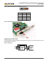
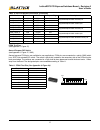
7 latticeecp3 pci express solutions board – revision a user’s guide table 5. Ispvm jtag connector (see appendix a, figure 21) 6 3 2 1 5 4 note: a dot denotes pin 1 on the both the pcb or back-panel bracket. Pin function color 1 pwr red 2 tdo brown 3 tdi orange 4 tms purple 5 gnd black 6 tck white fi...
Page 8
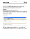
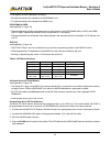
8 latticeecp3 pci express solutions board – revision a user’s guide download procedures requirements: • pc with ispvm system v.17.7 (or later) programming management software, installed with appropriate drivers (usb driver for usb cable, windows nt/2000/xp parallel port driver for ispdownload cable)...
Page 9
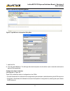
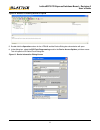
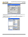
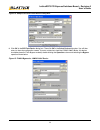
9 latticeecp3 pci express solutions board – revision a user’s guide figure 8. Ispvm fast programming mode figure 9. Ispvm device information dialog box 7. Add data file. 8. Click the green go button. This will begin the download process into the device. Upon successful download, the device will be o...
Page 10
10 latticeecp3 pci express solutions board – revision a user’s guide • d10 (green) will flash indicating tdi activity. • d8 (red) illuminated, this indicates that programn is low. • d7 (red) illuminated, this indicates that gsrn is low. Programn & gsrn (see appendix a, figure 23) • these push-button...
Page 11
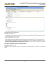
11 latticeecp3 pci express solutions board – revision a user’s guide figure 10. Results of scanning board via ispvm 5. Double-click the operation column for the lfe3-95 and the device dialog box shown below will open. 6. In the dialog box, select the spi flash programming mode in the device access o...
Page 12
12 latticeecp3 pci express solutions board – revision a user’s guide figure 12. Spi serial flash dialog screen 7. The spi serial flash device dialog box will open. In this box select spi flash erase, program, verify in the operation pull-down menu. 8. Select spi serial flash in the device family pul...
Page 13
13 latticeecp3 pci express solutions board – revision a user’s guide figure 14. Sample spi serial flash device dialog box 9. Click ok in the spi flash device dialog box. Then click ok in the select device dialog box. You will then return to the main configuration screen. If you do not desire to load...
Page 14
14 latticeecp3 pci express solutions board – revision a user’s guide figure 16. Programming main window 10.From the main programming window, select go in the top toolbar. This will begin the spi serial flash program- ming. Figure 17. Spi serial flash programming status window.
Page 15
15 latticeecp3 pci express solutions board – revision a user’s guide figure 18. Successful spi serial flash programming session on-board parallel spi flash memory (see appendix a, figure 24) • a 16-bit parallel flash device is also available. This board uses a lattice machxo cpld device to act as a ...
Page 16
16 latticeecp3 pci express solutions board – revision a user’s guide table 7. 100mhz clock destinations clock destination pcb designation destination pin cpld u12 a8 fpga u1 p21-pclkt2_0 fpga u1 k3-llum0-gdllt_in fpga u1 m4-pclkt7_0 serdes (see appendix a, figure 25) serdes/fpga reference clocks the...
Page 17
17 latticeecp3 pci express solutions board – revision a user’s guide fpga test pins (see appendix a, figure 27) general purpose dip switch (see appendix a, figure 27, sw5) general-purpose fpga pins are available for user applications. Fpga pins are connected to a switch (sw5) which is an spst side a...
Page 18
18 latticeecp3 pci express solutions board – revision a user’s guide figure 19. 8-position dip switch (sw5) on secondary pcb side general purpose leds (see appendix a, figure 27) leds are provided along the back panel edge of the pcb. These leds are connected to general-purpose fpga i/os. The leds a...
Page 19
19 latticeecp3 pci express solutions board – revision a user’s guide general-purpose header (see appendix a, figure 27, j5) a 2x9 header (j5) provides a general-purpose connection to communicate with general purpose fpga i/os. Table 13. General purpose header connections header pin fpga pin header p...
Page 20
20 latticeecp3 pci express solutions board – revision a user’s guide table 15. Logic analyzer to fpga pin reference signal fpga pin signal fpga pin la1 aa25 la2 y24 la3 w23 la4 w22 la5 aa26 la6 ab26 la7 w21 la8 w20 la9 ad26 la10 ad25 la11 aa24 la12 aa23 la13 ac26 la14 ac25 la15 y19 la16 y20 la17 ab2...
Page 21
21 latticeecp3 pci express solutions board – revision a user’s guide table 16. Cpld to fpga interconnections cpld pin fpga pin m1 b2 p13 b3 p10 d4 n7 e4 n8 c3 p11 d3 n13 g5 n1 g6 n3 e3 n4 f4 p1 h6 m12 j6 m2 c2 m3 d2 m4 k8 m6 j7 ordering information description ordering part number china rohs environ...
Page 22
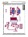
22 latticeecp3 pci express solutions board – revision a user’s guide appendix a. Schematic figure 20. Cover page 5 5 4 4 3 3 2 2 1 1 d d c c b b a a ti tl e siz e projec t re v d at e: sheet of 1605 valley center parkway bethlehem, pa 18017 ecp3 pci e de vkit eva l bo a rd 1. 0 co ve r pag e c 19 t ...
Page 23
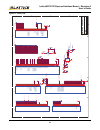
23 latticeecp3 pci express solutions board – revision a user’s guide figure 21. Power generation 5 5 4 4 3 3 2 2 1 1 d d c c b b a a gn d 1_8_t r im 12_0v 3_3v 3_3v gn d v cca _ t rim 12_0v 12_0v 12_0v 12_0v 1_8v 1_2v_a 3_3v 1_8v 3_3v v cc_ co re 12_0vi n 3_3v v cc_ co re 12_0v 3_3vi n 12_0v 12_0v 1...
Page 24
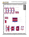
24 latticeecp3 pci express solutions board – revision a user’s guide figure 22. Power supplies 5 5 4 4 3 3 2 2 1 1 d d c c b b a a vc c _ c or e v cc_ co re vc c _pll 3_3v 1_2v_a 1_8v 3_3v 1_2v_a vc c _pll 3_3v ti tl e siz e projec t re v d at e: sheet of 1605 valley center parkway bethlehem, pa 180...
Page 25
25 latticeecp3 pci express solutions board – revision a user’s guide figure 23. Programming 5 5 4 4 3 3 2 2 1 1 d d c c b b a a config cfg switches spi flash on from ispvm cable this led indicates activity on tdi. Jtag fpga gsrn programn done indicator will light when configuration is successfully c...
Page 26
26 latticeecp3 pci express solutions board – revision a user’s guide figure 24. Parallel fpga loader 5 5 4 4 3 3 2 2 1 1 d d c c b b a a fl a s h_ a 2 1 fl a s h_ a 2 0 f lash _a19 fl a s h_ a 1 8 f lash _a17 f lash _a16 fl a s h_ a 1 5 fl a s h_ a 1 4 f lash _a13 f lash _a12 fl a s h_ a 1 1 f lash ...
Page 27
27 latticeecp3 pci express solutions board – revision a user’s guide figure 25. Serdes 5 5 4 4 3 3 2 2 1 1 d d c c b b a a pc sa_h d ou t p0 pc sa_h d ou t n 0 x 1_per p0 x 1_per n0 pc ie_3v3 x 1_per p0 x 1_per n0 pc ie_per st n x 1_pet p0 x 1_pet n0 pc ie_3v3 x 1_pc ie_c lkn x 1_pc ie_c lkp x 4_per...
Page 28
28 latticeecp3 pci express solutions board – revision a user’s guide figure 26. Ddr2 memory 5 5 4 4 3 3 2 2 1 1 d d c c b b a a ddr2 _ cs 0 # ddr2 _ ce 0 # ddr2 _ o dt0 d d r 2_d qs0 d d r 2_15 d d r 2_d q1 d d r 2_30 d d r 2_d q4 d d r 2_33 d d r 2_d q6 d d r 2_35 d d r 2_d q2 d d r 2_31 d d r 2_d ...
Page 29
29 latticeecp3 pci express solutions board – revision a user’s guide figure 27. Fpga test 5 5 4 4 3 3 2 2 1 1 d d c c b b a a ddr2 _ dq s 0 ddr2 _ 1 5 ddr2 _ dq 1 ddr2 _ 3 0 ddr2 _ dq 4 ddr2 _ 3 3 ddr2 _ dq 6 ddr2 _ 3 5 ddr2 _ dq 2 ddr2 _ 3 1 ddr2 _ dq 0 ddr2 _ 2 9 ddr2 _ dq 5 ddr2 _ 3 4 ddr2 _ dq 7...
Page 30
30 latticeecp3 pci express solutions board – revision a user’s guide figure 28. Vss/decoupling 5 5 4 4 3 3 2 2 1 1 d d c c b b a a seg0 seg1 la27 la33 la31 la25 la29 la17 la13 la23 la21 la5 la15 la11 la7 la19 la3 la1 la9 la34 la32 la22 la26 la16 la30 la14 la20 la12 la28 la24 la10 la6 la8 la4 la2 la1...
Page 31
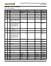
31 latticeecp3 pci express solutions board – revision a user’s guide appendix b. Bill of materials table 17. Bill of materials item quantity reference part manufacturer part number description 1 1 cn1 pci express x4 edge finger conn. Pcb edge finger 2 1 cn2 pci express x1 edge finger conn. Pcb edge ...
Page 32
32 latticeecp3 pci express solutions board – revision a user’s guide 26 2 j6, j7 sma molex 73391-0060 conn jack sma str 50 ohm pcb 27 1 la1 2_5767004-2 amp 2_5767004-2 conn recept 38pos .025 vert smd 28 5 lp1, lp2, lp3, lp4, lp5 5016 keystone electronics 5016 test point pc compact smt 29 3 mh1, mh2,...
Page 33
33 latticeecp3 pci express solutions board – revision a user’s guide 52 1 r55 2_2k-0603smt panasonic erj-3geyj222v res 2.2k ohm 1/10w 5% 0603 smd 53 2 r62, r72 1k_adj/smt3mm murata pvg3a102c01r00 pot 1k 3mm cerm sq s/t smd 54 0 r65(deleted) 0r-2010smt vishay/dale crcw20100000z0ef res 0.0 ohm1/2w 5% ...
Page 34
34 latticeecp3 pci express solutions board – revision a user’s guide 83 1 r227 1_6r-0603smt panasonic erj-3geyj1r6v resistor 1.6 ohm 1/10w 5% 0603 84 4 r223, r224, r228, r229 50r-0402smt vishay fc0402e50r0btbst1 res 50 ohm 50mw .1% 0402 smd 85 1 y2 crystek_133mhz crystek ccld-033-50-133.000 osc lvds...
Page 35: Mouser Electronics
Mouser electronics authorized distributor click to view pricing, inventory, delivery & lifecycle information: lattice : lfe3-95ea-sp-evn lfe3-95ea-pcie-dkn.


