- DL manuals
- Lattice Semiconductor
- Motherboard
- LFSC80E-P4-EV
- User Manual
Lattice Semiconductor LFSC80E-P4-EV User Manual
Summary of LFSC80E-P4-EV
Page 1
September 2009 revision: eb31_01.2 latticesc pci express x4 evaluation board user’s guide.
Page 2
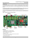
2 latticesc pci express x4 evaluation board lattice semiconductor user’s guide introduction this user’s guide describes the latticesc pci express x4 evaluation board featuring the latticesc lfscm3ga80ep1-6fc1152c fpga device. This stand-alone evaluation pcb provides a functional platform for develop...
Page 3
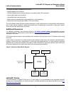
3 latticesc pci express x4 evaluation board lattice semiconductor user’s guide • on-board and external reference clock sources • interchangeable clock oscillators • orcastra demonstration software interface via standard ispvm jtag connection • various high-speed layout structures • user-defined inpu...
Page 4
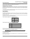
4 latticesc pci express x4 evaluation board lattice semiconductor user’s guide note: the connections referenced in this document refer to the lfscm3ga80 device. Available i/os and associ- ated sysio™ banks may differ for other densities within this device family. Applying power to the board the latt...
Page 5
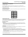
5 latticesc pci express x4 evaluation board lattice semiconductor user’s guide programming/fpga configuration (see appendix a, figure 7) a programming header is provided on the evaluation board, providing access to the latticesc jtag port. Note: an ispdownload ® cable is included with each isplever ...
Page 6
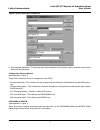
6 latticesc pci express x4 evaluation board lattice semiconductor user’s guide 4. Press the scan button located in the toolbar. The latticesc device should be automatically detected. Figure 3. Ispvm main window 5. Double-click the device to open the device information dialog. In the device informati...
Page 7
7 latticesc pci express x4 evaluation board lattice semiconductor user’s guide figure 4. Device information dialog box 6. Click the green go button. This will begin the download process into the device. Upon successful download, the device will be operational. Configuration status indicators (see ap...
Page 8
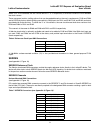
8 latticesc pci express x4 evaluation board lattice semiconductor user’s guide mode [3:0] (see appendix a, figure 7) the fpga mode pins are set on the board for a particular programming mode via the sw6 dip switch. Jtag pro- gramming is independent of the mode pins and is always available to the use...
Page 9
9 latticesc pci express x4 evaluation board lattice semiconductor user’s guide when y3 or y5 are enabled, the user should remove y1 or y4 respectively to eliminate contention issues between the clock sources. There are several resistor stuffing options that may be needed based on the user’s requirem...
Page 10
10 latticesc pci express x4 evaluation board lattice semiconductor user’s guide pci express x1 cable connectors pci express x1 cable connectors (con1 and con2) are provided to demonstrate cable capabilities of the serdes channels. These cable connectors conform with the pci express cable specificati...
Page 11
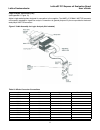
11 latticesc pci express x4 evaluation board lattice semiconductor user’s guide logic analysis connection (la1) (see appendix a, figure 13) agilent single-ended probes designed for connection to the supplies. Tyco/amp’s 2-767004-2 mictor connector can be easily attached for signal bus analysis. Conn...
Page 12
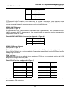
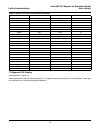
12 latticesc pci express x4 evaluation board lattice semiconductor user’s guide 17-segment led display (see appendix a, figure 12) general-purpose fpga pins are connected to a 17-segment display according to the following table. These pins can be driven low to illuminate the display segments. Pr80d ...
Page 13
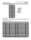
13 latticesc pci express x4 evaluation board lattice semiconductor user’s guide table 11. 17-segment led display segment bga a ac33 b aa30 c ad34 d aa28 e aa33 f ab34 g aa29 h y31 k y32 m w24 n w33 p y34 r w26 s v34 t w25 u u33 dp y27 a b c d g f e dp h t s r k m n u p test sma connections general-p...
Page 14
14 latticesc pci express x4 evaluation board lattice semiconductor user’s guide high speed test point dp1 (see appendix a, figure 12) general-purpose fpga pins are available via a differential test pad. These connections allow a high-impedance probe to measure the performance of a coupled- different...
Page 15
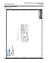
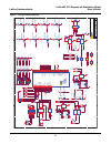
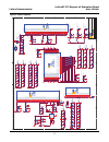
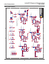
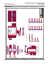
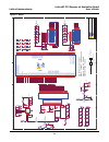
15 latticesc pci express x4 evaluation board lattice semiconductor user’s guide appendix a. Schematics figure 6. 5 5 4 4 3 3 2 2 1 1 d d c c b b a a ti tl e siz e projec t r ev d at e: sheet of sc8 0 x4 pci express ca rd 3. 0 c o v e r p age c 11 1 ti tl e siz e projec t r ev d at e: sheet of sc8 0 ...
Page 16
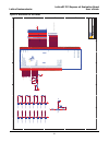
16 latticesc pci express x4 evaluation board lattice semiconductor user’s guide figure 7. Configuration/testpoints 5 5 4 4 3 3 2 2 1 1 d d c c b b a a q_1 sc sn _1 sc sn tck loc al_t d i loc al_t c k loc al_t m s pr ogr am n tms loc al_t d o tck local_t do tdi_b uf tms initn do ne cs 0 n wrn cs 1 gr...
Page 17
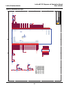
17 latticesc pci express x4 evaluation board lattice semiconductor user’s guide figure 8. Power supplies 5 5 4 4 3 3 2 2 1 1 d d c c b b a a mc_ v re f_ re g vt t _6_7 vt t _2_3 vt t _2_3 vt t _6_7 v cc_ co re 1_2v 1_5v 1_5v 1_5v v ddrx vd d t x 2_5v vd d p vd d r x v ddp vd d t x 1_2v vd d p vd d r...
Page 18
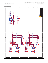
18 latticesc pci express x4 evaluation board lattice semiconductor user’s guide figure 9. Dc/dc conversion 5 5 4 4 3 3 2 2 1 1 d d c c b b a a 2_5_tr im core _trim 1_2_tr im vc c a 3_3_tr im vc c a 12_0v gn d 12_0v vc c a 12_0v 2_5v 3_3v 12_0v v cc_ co re 1_5v 2_5v 12_0v 1_2v 1_8v 12_0v 12_0v v cc_ ...
Page 19
19 latticesc pci express x4 evaluation board lattice semiconductor user’s guide figure 10. Serdes 5 5 4 4 3 3 2 2 1 1 d d c c b b a a b_h d in p1_r pet p2 50 b_h d in n 1_r pet n2 50 b_h d in p2_r pet p1 50 b_h d in n 2_r pet n1 50 b_h d in p3_r pet p0 50 b_h d in p0_r pet p3 50 b_h d in n 3_r pet n...
Page 20
20 latticesc pci express x4 evaluation board lattice semiconductor user’s guide figure 11. Ddr2 5 5 4 4 3 3 2 2 1 1 d d c c b b a a m em int f_ba1 m em int f_ba0 me min tf_ ra s # me min tf_ we # me min tf_ ca s # me min tf_ a 5 me min tf_ a 3 me min tf_ a 0 me min tf_ a 8 me min tf_ a 4 me min tf_ ...
Page 21
21 latticesc pci express x4 evaluation board lattice semiconductor user’s guide figure 12. Differential i/o test smas 5 5 4 4 3 3 2 2 1 1 d d c c b b a a lvd s_i n p_0 lvd s_i n n _0 lvd s_i n p_1 lvd s_i n n _1 lvd s_i n p_2 lvd s_i n n _2 lvd s_i n p_3 lvd s_i n n _3 lvd s_ou t p_0 lvd s_ou t p_1 ...
Page 22
22 latticesc pci express x4 evaluation board lattice semiconductor user’s guide figure 13. Differential i/o loops 5 5 4 4 3 3 2 2 1 1 d d c c b b a a loop_p11 loop_n 11 loop_p4 loop_n 4 loop_p0 loop_n 0 loop_p5 loop_n 5 loop_p12 loop_n 12 loop_p6 loop_n 6 loop_p13 loop_n 13 loop_p7 loop_n 7 loop_n 1...
Page 23
23 latticesc pci express x4 evaluation board lattice semiconductor user’s guide figure 14. Clocks 5 5 4 4 3 3 2 2 1 1 d d c c b b a a osc _ in _2 osc _ in _4 osc _ in _1 b_osc _n a_osc _n a_osc _p b_osc _p 3_3v 3_3v 3_3v 3_3v 3_3v 3_3v 3_3v 3_3v osc _i n _2 [8 ] osc _ in _1 [7 ] osc _ in _4 [2 ] b_r...
Page 24
24 latticesc pci express x4 evaluation board lattice semiconductor user’s guide figure 15. Vss decoupling 5 5 4 4 3 3 2 2 1 1 d d c c b b a a v cc_ co re 1_5v v ddrx vd d t x 2_5v vd d p v cc_ co re 1_2v 2_5v 2_5v 2_5v 2_5v 2_5v 2_5v 1_8v 1_8v sc _vt t ti tl e siz e projec t r ev d at e: sheet of sc...
Page 25
25 latticesc pci express x4 evaluation board lattice semiconductor user’s guide figure 16. Parallel flash 5 5 4 4 3 3 2 2 1 1 d d c c b b a a f lash _a9 f lash _a8 f lash _a7 f lash _a6 f lash _a5 f lash _a4 fl a s h_ we _ n fl a s h_ wp _ n fl a s h_ o e _ n t m s_xo tdi_ x o tdo _ x o f lash _a3 f...


