- DL manuals
- Lattice Semiconductor
- Motherboard
- XP2 Advanced
- User Manual
Lattice Semiconductor XP2 Advanced User Manual
Summary of XP2 Advanced
Page 1
March 2011 revision: eb30_01.5 latticexp2 advanced evaluation board user’s guide.
Page 2
2 latticexp2 advanced lattice semiconductor evaluation board user’s guide introduction the latticexp2™ advanced evaluation board provides a convenient platform to evaluate, test and debug user designs and ip cores targeted for the latticexp2-17 fpga. The board features of a latticexp2-17 fpga in a 4...
Page 3
3 latticexp2 advanced lattice semiconductor evaluation board user’s guide • prototyping areas with access to 14 i/o pins • selectable i/o bank voltages • four pairs of sma connectors for high speed differential signals • oscillator socket for both half-size and full-size oscillators • 3.3v, 2.5v, 1....
Page 4
4 latticexp2 advanced lattice semiconductor evaluation board user’s guide while, it’s best to put it back in the static shielding bag. Please save the static shielding bag and packing box for future storage of the board when it is not in use. When reaching for the board, it is recommended that you f...
Page 5
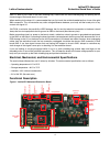
5 latticexp2 advanced lattice semiconductor evaluation board user’s guide latticexp2 device this board features a latticexp2 fpga with a 1.2v dc core in a 484-ball fpbga package. The default device is the latticexp2-17. Any other latticexp2 density in this package can be accommodated. A complete des...
Page 6
6 latticexp2 advanced lattice semiconductor evaluation board user’s guide for the vcc_adj adjustable voltage, the isppac-powr1220at8 will detect the voltage rail and show the status using five leds. Each of these five leds indicates a particular voltage range. If the vcc_adj is in one of the volt- a...
Page 7
7 latticexp2 advanced lattice semiconductor evaluation board user’s guide table 7. Mixed voltage i/o support v ccio input sysio standards output sysio standards 1.2v 1.5v 1.8v 2.5v 3.3v 1.2v 1.5v 1.8v 2.5v 3.3v 1.2v yes yes yes yes 1.5v yes yes yes yes yes 1.8v yes yes yes yes yes 2.5v yes yes yes y...
Page 8
8 latticexp2 advanced lattice semiconductor evaluation board user’s guide prototype areas for general purpose i/o testing or monitoring, numerous test points are provided for direct access. Some test points are grouped together and arranged in a grid pattern according to their associated i/o bank an...
Page 9
9 latticexp2 advanced lattice semiconductor evaluation board user’s guide the 16-pin socket will allow connection to pll clock pin a2 when the top of the oscillator is aligned to socket pins 1 and 16. Note that the sma connector j12 is shared with the on-board oscillator. When installing the oscilla...
Page 10
10 latticexp2 advanced lattice semiconductor evaluation board user’s guide table 11. Jtag programming headers pin separate programming chained programming jumper on j49 (none on j45) jumper on j45 (none on j49) j39 function j40 function j39 function j40 function 1 vcc (3.3v) vcc (3.3v) vcc (3.3v) no...
Page 11
11 latticexp2 advanced lattice semiconductor evaluation board user’s guide sw2 and sw8 on the right side and the upper side of the board are 8-pin dip switches. The pull-up resistors asso- ciated with these switches are wired to 3.3v. A switch in the down position produces a low (0), the up position...
Page 12
12 latticexp2 advanced lattice semiconductor evaluation board user’s guide seven segment display the 7-segment led located near the eight leds is controlled by latticexp2 bank 4 i/o pins. The connections of the segments are shown in figure 3. Figure 3. 7-segment display lcd the lcd module connector ...
Page 13
13 latticexp2 advanced lattice semiconductor evaluation board user’s guide lumex: • lcm-s01601 series: 16 characters x 1 line • lcm-s00802 series: 8 characters x 2 lines • lcm-s01602 series: 16 characters x 2 lines • lcm-s02002 series: 20 characters x 2 lines • lcm-s02402 series: 24 characters x 2 l...
Page 14
14 latticexp2 advanced lattice semiconductor evaluation board user’s guide table 19. Video rx mdr connections pin # function latticexp2 i/o pin # function latticexp2 i/o 1 — — 14 rx_in3_p y3 2 gnd — 15 rx_in3_n w3 3 — — 16 — — 4 rx_clkin_p p1 17 gnd — 5 rx_clkin_n r1 18 — — 6 — — 19 — — 7 — — 20 rx_...
Page 15
15 latticexp2 advanced lattice semiconductor evaluation board user’s guide usb 1.1 for implementing the usb interface, the latticexp2 board contains a usb 1.1 transceiver max3454eete (or ncn2500mnr2 from on semiconductor), a type-a connector and a type-b usb connector. Note there is a third usb conn...
Page 16
16 latticexp2 advanced lattice semiconductor evaluation board user’s guide ps/2 mouse the ps/2 mouse connector (jp1) on this board connects the clock and data through the pca9306 level translator to the latticexp2. The clock and data are connected as described in table 24. Table 24. Connections betw...
Page 17
17 latticexp2 advanced lattice semiconductor evaluation board user’s guide ddr2_dq6 t21 3 14 ddr2_dq7 t20 3 16 ddr2_dm0 p16 3 10 ddr2_dqs0_p t22 3 13 ddr2_dqs0_n u22 3 11 ddr2_dq8 k21 3 23 ddr2_dq9 l21 3 25 ddr2_dq10 m19 3 35 ddr2_dq11 m20 3 37 ddr2_dq12 m17 3 20 ddr2_dq13 m16 3 22 ddr2_dq14 m21 3 3...
Page 18
18 latticexp2 advanced lattice semiconductor evaluation board user’s guide ethernet phy in the upper middle portion of the board is u11, a national semiconductor gigabit ethernet phy (dp83865). The latticexp2 fpga interacts with the phy over a media independent interface (mii). The phy is connected ...
Page 19
19 latticexp2 advanced lattice semiconductor evaluation board user’s guide table 27. 10/100/1000 ethernet phy connection summary description latticexp2 i/o sysio bank eth_clk_to_mac g11 1 eth_col a17 1 eth_crs b16 1 eth_egp0 (low, install r91 to pull high) -- eth_egp2 g13 1 eth_egp4 g14 1 eth_egp5 d...
Page 20
20 latticexp2 advanced lattice semiconductor evaluation board user’s guide table 28. Pci connector component side j11 pin# signal i/o description latticexp2 connection 1 12v vcc 12v voltage supply pin — 2 tck - pci jtag tck signal — 3 gnd vss system ground gnd 4 tdo - jtag tdo signal — 5 5v vcc 5v v...
Page 21
21 latticexp2 advanced lattice semiconductor evaluation board user’s guide 47 ad[12] i/o pci address and data bit 12 aa9 48 ad[10] i/o pci address and data bit 10 y9 49 m66en o pci 66 mhz enable — 52 ad[8] i/o pci address and data bit 8 ab11 53 ad[7] i/o pci address and data bit 7 aa11 54 +3.3v vcc ...
Page 22
22 latticexp2 advanced lattice semiconductor evaluation board user’s guide 4-input adc u3 is the quad adc (analog to digital converter) ads7842 ic. The four analog inputs ain0 to ain3 are rc filtered versions of the external analog signals applied at j10. The full scale values for the adc inputs wil...
Page 23
23 latticexp2 advanced lattice semiconductor evaluation board user’s guide table 30. Adc connections description latticexp2 i/o sysio bank d0 h3 7 d1 h4 7 d2 g3 7 d3 g2 7 d4 h1 7 d5 h2 7 d6 g6 7 d7 h6 7 d8 h5 7 d9 j5 7 d10 j1 7 d11 j2 7 a0 f3 7 a1 e5 7 clk f2 7 busyn f1 7 wrn g1 7 csn f5 7 rdn f4 7 ...
Page 24
24 latticexp2 advanced lattice semiconductor evaluation board user’s guide usb download the evaluation board has a usb download cable built in. The built-in cable consists of a usb type-b connector (j33), a usb microcontroller, and a machxo device. To use the built-in download cable, simply connect ...
Page 25
25 latticexp2 advanced lattice semiconductor evaluation board user’s guide the following device programming sections provide procedures for programming the on-board spi flash using either a standard usb cable, or an ispdownload cable (parallel or usb). If you would like to program the latticexp2 sra...
Page 26
26 latticexp2 advanced lattice semiconductor evaluation board user’s guide open as shown in figure 6. Select device access options and spi flash programming as shown in figure 7. Figure 6. Device information dialog figure 7. Spi serial flash device dialog 8. Select browse and point to the location o...
Page 27
27 latticexp2 advanced lattice semiconductor evaluation board user’s guide figure 8. Select device dialog 10. Check that the spi serial flash device window now appears as shown in figure 9, then press ok to close the spi serial flash device window. Figure 9. Spi serial flash device dialog 11. Check ...
Page 28
28 latticexp2 advanced lattice semiconductor evaluation board user’s guide figure 10. Device information dialog 12. Check that the lsc ispvm system window appears as it does in figure 11. Figure 11. Ispvm system interface 13. To begin the download of the bitstream into the spi flash, press the go me...
Page 29
29 latticexp2 advanced lattice semiconductor evaluation board user’s guide latticexp2 sram configuration using spi flash and a lattice ispdownload cable at j40 the latticexp2 sram can be configured easily via the on board spi flash using the jtag port and ispvm. The latticexp2 device is sram-based, ...
Page 30
30 latticexp2 advanced lattice semiconductor evaluation board user’s guide figure 13. Device information dialog figure 14. Spi serial flash device dialog 8. Select browse and point to the location of the bitstream file. Note that if you have a “.Jed” file output from isp- lever, you can convert it t...
Page 31
31 latticexp2 advanced lattice semiconductor evaluation board user’s guide figure 15. Select device dialog 10. Check that the spi serial flash device window now appears as shown in figure 16, then press ok to close the spi serial flash device window. Figure 16. Spi serial flash device dialog 11. Che...
Page 32
32 latticexp2 advanced lattice semiconductor evaluation board user’s guide figure 17. Device information dialog 12. Check that the lsc ispvm system window appears as it does in figure 18. Figure 18. Ispvm system interface 13. To begin the download of the bitstream into the spi flash, press the go me...
Page 33
33 latticexp2 advanced lattice semiconductor evaluation board user’s guide ordering information description ordering part number china rohs environment-friendly use period (efup) latticexp2 advanced evaluation board (rohs compliant) lfxp2-17e-h-evn latticexp2 advanced evaluation board (non-rohs, obs...
Page 34
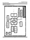
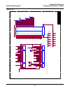
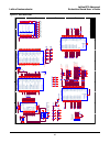
34 latticexp2 advanced lattice semiconductor evaluation board user’s guide appendix a. Schematic figure 19. 5 5 4 4 3 3 2 2 1 1 d d c c b b a a title si z e do c u m e n t nu m b e r re v d a te: s heet o f b lattic e x p 2 advanc ed engineering board 484 f pbg a a 11 4 title si z e do c u m e n t n...
Page 35
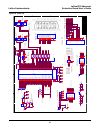
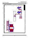
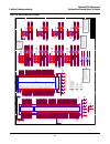
35 latticexp2 advanced lattice semiconductor evaluation board user’s guide figure 20. 5 5 4 4 3 3 2 2 1 1 d d c c b b a a v c c _ 3. 3v rx _ in 0 _ n rx _ in 0 _ p rx _ in 3 _ n rx _ in 1 _ n rx _ in 3 _ p rx _ in 1 _ p rx _ in 2 _ n rx _ in 2 _ p r x _c lki n _n r x _c lki n _p tx _ o ut1 _ n tx _ ...
Page 36
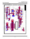
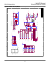
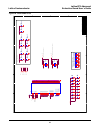
36 latticexp2 advanced lattice semiconductor evaluation board user’s guide figure 21. 5 5 4 4 3 3 2 2 1 1 d d c c b b a a vc c _ 3 .3 v lv _c t s_n lv _r t s_n lv _t x d lv _r x d hv _ r x d hv _ tx d h v _r t s_n hv _ c ts _ n r s232_c t s_n r s232_0 r s232_r x d r s232_1 r s232_t x d r s232_2 r s2...
Page 37
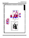
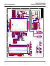
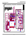
37 latticexp2 advanced lattice semiconductor evaluation board user’s guide figure 22. 5 5 4 4 3 3 2 2 1 1 d d c c b b a a vc c _ 3 .3 v xp2 _ t c k xp2 _ t d i pw r _ a t d i pw r _ t m s vc c _ 3 .3 v xp2 _ t d o pw r _ t d o xp2 _ t m s pw r _ t c k xp2 _ d o n e x p 2 _ in it n vc c _ 3 .3 v cfg ...
Page 38
38 latticexp2 advanced lattice semiconductor evaluation board user’s guide figure 23. 5 5 4 4 3 3 2 2 1 1 d d c c b b a a pc i_ a d 3 0 pc i_ a d 1 6 p c i_ irdy _ n pc i_ a d 8 pci_ad 26 pci_ad 28 pci_ad 30 pci_m 66en pci_ad 16 pc i_ vi o pci_ad 15 pci_ad 1 pci_ad 3 pci_c lk pc i_ vi o pc i_ t r d ...
Page 39
39 latticexp2 advanced lattice semiconductor evaluation board user’s guide figure 24. 5 5 4 4 3 3 2 2 1 1 d d c c b b a a cf_ io rd cf3 1 c f _v s1 c f 30 cf_ ce 2 cf2 9 c f _c d 1 c f 23 c f _d 03 cf0 c f _d 04 cf1 c f _d 05 cf2 cf[0 ..4 5 ] c f _d 06 cf3 c f _d 07 cf4 c f _d 00 cf1 8 c f _d 01 cf1...
Page 40
40 latticexp2 advanced lattice semiconductor evaluation board user’s guide figure 25. 5 5 4 4 3 3 2 2 1 1 d d c c b b a a l cd_ rs l cd5 lc d _e lc d 6 l cd_ db 1 l cd7 l cd_ db 3 l cd8 l cd_ db 5 l cd9 l cd_ db 7 l cd1 0 lc d _r /w lc d 0 lc d _d b0 lc d 1 lc d _d b2 lc d 2 lc d _d b4 lc d 3 lc d _...
Page 41
41 latticexp2 advanced lattice semiconductor evaluation board user’s guide figure 26. 5 5 4 4 3 3 2 2 1 1 d d c c b b a a p h y_r x _d 4 p h y_r x _d 5 et h _r x _d 4 p h y_r x _d 7 p h y_r x _d 6 et h _r x _d 7 et h _r x _d 5 et h _r x _d 6 ph y _ c r s ph y _ c o l mdi_ p 3 mdia _ b u s 4 mdi_ p 2...
Page 42
42 latticexp2 advanced lattice semiconductor evaluation board user’s guide figure 27. 5 5 4 4 3 3 2 2 1 1 d d c c b b a a u sb_p a5 u sb_p a4 u sb_p a3 u sb_p a2 u sb_p a1 u sb_p a0 u sb_p a7 u sb_p a6 u sb_p a5 u sb_p a4 u sb_p a3 u sb_p a2 u sb_p a1 u sb_p a0 u sb_p d 7 us b + us b - u sb_p d 6 u ...
Page 43
43 latticexp2 advanced lattice semiconductor evaluation board user’s guide figure 28. 5 5 4 4 3 3 2 2 1 1 d d c c b b a a vt t vc c _ 1 .8 v ddr2 _ dm0 s o dimm_ d q 8 ddr2 _ dq 6 ddr2 _ dq 7 ddr2 _ dq 2 ddr2 _ dq 3 ddr2 _ dm0 ddr2 _ dq s 0 _ n ddr2 _ dq s 0 _ p s o dimm_ d q 3 1 s o dimm_ d q 2 5 s...
Page 44
44 latticexp2 advanced lattice semiconductor evaluation board user’s guide figure 29. 5 5 4 4 3 3 2 2 1 1 d d c c b b a a vc c _ 3 .3 v vc c _ 2 .5 v vc c _ a d j vc c _ 1 .8 v vc c _ 3 .3 v vc c _ 1 .2 v vc c _ 1 .8 v vc c _ 2 .5 v vc c _ a d j vc c _ 1 .2 v vc c _ 3 .3 v vc c _ 1 .2 v vc c _ 1 .8 ...
Page 45
45 latticexp2 advanced lattice semiconductor evaluation board user’s guide figure 30. 5 5 4 4 3 3 2 2 1 1 d d c c b b a a vc c _ in vc c _ in p w r _ good _3. 3v p w r _ good _2. 5v p w r _ good _1. 8v p w r _ good _1. 2v p w r_ g o o d_ v re f p w r_ g o o d_ v t t ad j _3. 3v ad j _2. 5v ad j _1. ...
Page 46
46 latticexp2 advanced lattice semiconductor evaluation board user’s guide figure 31. 5 5 4 4 3 3 2 2 1 1 d d c c b b a a gat e_1. 2 vc c _ 1 .2 v vc c _ 2 .5 v dra in _ 2 .5 pw r _ a d j p w r _3. 3v _10a gat e_2. 5 dra in _ 2 .5 pw r _ 3 .3 v_ 1 0 a gat e_1. 2 dra in _ 1 .2 pw r _ 3 .3 v_ 1 0 a ga...
Page 47
47 latticexp2 advanced lattice semiconductor evaluation board user’s guide figure 32. 5 5 4 4 3 3 2 2 1 1 d d c c b b a a ti tl e siz e d o c u m e nt n u m b er re v d at e: sheet of b p lacem ent & di m e nsi o n (6.0" x 12.0" ) c 14 14 ti tl e siz e d o c u m e nt n u m b er r ev d at e: sheet of...
Page 48: Mouser Electronics
Mouser electronics authorized distributor click to view pricing, inventory, delivery & lifecycle information: lattice : lfxp2-17e-h-evn.


