- DL manuals
- Loewe
- DVD Player
- Xemix 6222
- Service Manual
Loewe Xemix 6222 Service Manual
Summary of Xemix 6222
Page 1
Contents section 1 . . . . Summary section 2 . . . . Cabinet & main chassis section 3 . . . . Electrical section 4 . . . . Parts list.
Page 2: Section 1
Section 1 summary contents product safety servicing guidelines for video products ............. 1-3 servicing precautions .................................................................................................. 1-4 • general servicing precautions • insulation checking prodedure • electrost...
Page 3
1-3 caution : do not attempt to modify this product in any way, never perform customized installations without manufac- turer’s approval. Unauthorized modifications will not only void the warranty, but may lead to your being liable for any resulting property damage or user injury. Service work shoul...
Page 4: Servicing Precautions
1-4 servicing precautions caution : before servicing the dvd covered by this service data and its supplements and addends, read and follow the safety precautions. Note : if unforeseen circum- stances create conflict between the following servicing pre- cautions and any of the safety precautions in t...
Page 5: Specifications
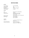
1-5 specifications • general power requirements ac 110~240v, 50/60hz power consumption 14w dimensions(approx.) 360 x 69 x 215mm (w/h/d) mass(approx.) 2.52kg operating temperature 5˚c to 35˚c (41˚f to 95˚f) operating humidity 5% to 90% • system laser semiconductor laser, wavelength 650nm signal syste...
Page 6
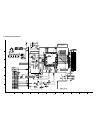
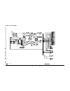
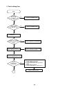
3-35 3-36 4. Front circuit diagram system not operate remocon not operate power led abnormal digital abnormal system not operate or dihitron abnormal or key not operate.
Page 7
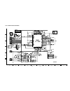
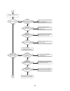
3-31 3-32 system not working or digitron not display program download fail 2.5 doesn't appear system not working digitron all not display system not working video signal not appeared no power on video signal y video signal color system not working or screen is abnormal 2. System circuit diagram.
Page 8
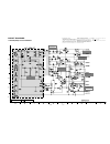
3-29 3-30 circuit diagrams 1. Power(smps) circuit diagram important safety notice when servicing this chassis, under no cir- cumstances should the original design be modified or altered without permission from the loewe corporation. All compo- nents should be replaced only with types identical to th...
Page 9
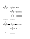
3-33 3-34 3. Rf & servo circuit diagram cd/dvd ld will not on.
Page 10: Section 2
2-1 section 2 cabinet & main chassis contents 1. Exploded views ................................................................................................................2-2 1. Cabinet and main frame section .........................................................................................
Page 11: Exploded Views
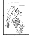
2-2 exploded views 1. Cabinet and main frame section 467 300 a48 452 452 465 465 457 275 332 optional part 463 463 463 463 463 a46 250 463 260 a43 a00 283 a49 a42 280 a 5 4 3 2 1 b c d.
Page 12
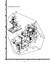
2- 3 2. Deck mechanism section 001 003 004 431 026 021 023 025 436 436 436 022 024a 024b 024a 435 022a 032 024 027 028 031 030 434 a02 a03 a01 a00 020 011a 010 015 015a 015b 015c 017 013 014 018 011 029 012 430 431 431 012 430 433 002 a 5 4 3 2 1 b c d.
Page 13
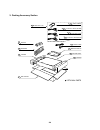
3. Packing accessory section battery 808 packing sheet 804 packing optional parts 803 806 820 owner’s manual cable, coaxil 810 cable ass’y (rf) 801 remocon 900 box carton 802 packing 803 811 812 plug ass’y 1way(yellow) plug ass’y 1way(black) plug ass’y 2way 821 scart cable 2- 4.
Page 14
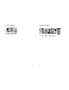
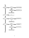
3-37 3-38 5. Audio circuit diagram 2ch audio 2ch audio out bad 2ch audio out bad.
Page 15
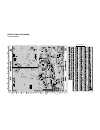
3-49 3-50 3. Key p.C.Board (left) (solder side) 4. Key p.C.Board (right) location guide (solder side).
Page 16
3-47 3-48 2. I/o p.C.Board location guide.
Page 17
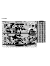
3-45 3-46 printed circuit diagrams 1. Main p.C.Board location guide.
Page 18
3-39 3-40 6. Jack circuit diagram all video signal isn't appear or bad video signal cvbs 2ch audio video signal y video signal color.
Page 19: Section 3
3-1 section 3 electrical contents electrical troubleshooting guide ......................................................................3-2 1. Power check flow.....................................................................................................................3-2 2. System operation...
Page 20
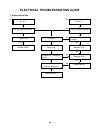
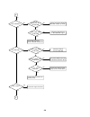
3-2 electrical troubleshooting guide no 5v_a . No 5.2va. Is 5.2va section working? Is 5.2v present at emitter of q107? Replace q107. Is there a dc voltage at (+) terminal of bd101? Is there a dc voltage at r101? Replace ic101. Check f101 1. Power check flow no vf+ is 5.2va section working? Replace d...
Page 21
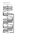
3-3 2. System operation flow power on no yes yes yes no no no show logo tray closed? Tray close to closed position sled moves to inner position recieve open/ close key? Receive close key? 1. Stop playback & open tray 2. Display tray open message & logo 1. Execute pressed key & ir key 2. Systemoperat...
Page 22
3-4 3. Test & debug flow test check the power part no yes no yes no no no yes yes check the power part check the regulators or diode(d501). Check the connector connection main pcb & communication signal 1. Check 27mhz system clock. 2. Check systemreset circuit. 3. Check flash r/wenable signal prd, r...
Page 23
3-5 a b reset or power on. No yes yes yes yes yes yes yes yes no no no no no no no no show logo? Flash memory operates properly? Check connecti on lines between flash & mt1379 and the flash access time whether is sui table or not. Sdram works properl y? Mt1379 video outputs properly? Have tv signal ...
Page 24
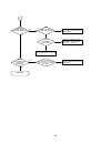
3-6 b no no yes yes yes no yes yes yes no yes no no no does the sled move to inner side when it is at outter positi on? Motor driver stby pin is high? Motor driver stby pin is high? Sl+ and sl- output properl y? Optical lens has movements for searching focus? Proper f+ & f- outputs? Check cable conn...
Page 25
3-7 c no no no no no no no yes yes yes yes yes yes yes yes yes no no laser turns on when reading disc? Ld01 or ld02 output properly? Check the laser power circuit on mt1336 and connecting to power transistor. (q204, q205) check therel ated ci rcuit on laser power transi stor check the related circui...
Page 26
3-8 d yes yes no no yes yes yes yes yes yes yes no no no no no focus on ok? Track on ok? Disc is play? E proper signals on a, b, c, d of mt1336 check connections between mt1336 and pick-up head. Proper feo signal on mt1336? Proper feo signal on mt1336? Check the related circuit on mt1336 feo sugnal ...
Page 27
3-9 e normal audio output when disc playback? Normal ir. Vfd & front pannel key functions? Test end audio dac received correct data stream? Normal audio dac out? (ic601) check audio filter, amplify, mute circuit. (ic401 application circuit)? Check connection between mt1379 & audio dac. (check vrst#,...
Page 28
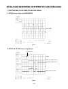
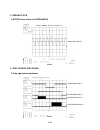
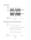
3-10 details and waveforms on system test and debugging 1. System 27mhz clock,reset,flash r/w signal 1) mt1379 main clock is at 27mhz(x501) 3.8v, 27mhz fig 1-1 2) mt1379 & mt1336 reset is high active. Pwr_ctl(p5901 pin 17) 5.2va power cord in m_reset(p5901 pin 19) urst(ic501 pin 188) fig 1-2.
Page 29
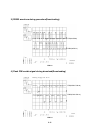
3-11 3) rs232 waveform during procedure(downloading) txd(j6 pin3) rxd(j6 pin 2) fig 1-3 4) flash r/w enable signal during download(downloading) frd(ic5a1 pin 28) fwr(ic5a1 pin 11) fig 1-4.
Page 30
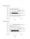
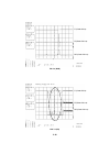
3-12 2. Sdram clock 1) mt1379 main clock is at 27mhz(x501) (ic502,ic503 pin 35) dclk = 93mhz, vp-p=2.2, vmax=2.7v fig 2-1 3. Tray open/close signal 1) tray open/close waveform open((cn203 pin 3) close(cn203 pin 2) tropen(ic202 pin 1) trclose(ic202 pin 2) fig 3-1.
Page 31
3-13 2) tray close waveform open((cn203 pin 3) close(cn203 pin 2) tropen(ic202 pin 1) trclose(ic202 pin 2) fig 3-2 3) tray open waveform open((cn203 pin 3) close(cn203 pin 2) tropen(ic202 pin 1) trclose(ic202 pin 2) fig 3-3.
Page 32
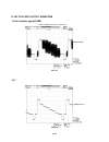
3-14 4. Sled control related signal (no disc condition) fmso(2.0v/1.4v/1.0v) (ic501 pin 19) stby(5v) – (ic201 pin 50) sl+(4.7v/3.6v/1.9v) (ic202 pin 12) sl-(5.3v/3.7v/2.5v) (ic202 pin 13) fig 4-1 5. Lens control related signal(no disc condition) foso(1.5v/1.4v/1.3v) (ic501 pin 12) f+(4.0v/3.6v/3.2v)...
Page 33
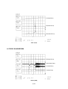
3-15 6. Laser power control related signal(no disc condition) mdi1(0v/180mv) (ic201 pin 124) ld01(5.0v//3.5v) ic201 pin 125) ld02(5.0v/3.6v) (ic201 pin 126) fig 6-1 7. Disc type judgement waveform f+(ic202 pin 9) fe(ic201 pin 18) rfl(ic201 pin 19) fig 7-1 (dvd).
Page 34
3-16 f+(ic202 pin 9) fe(ic201 pin 18) rfl(ic201 pin 19) fig 7-2 (dvd) f+(ic202 pin 9) fe(ic201 pin 18) rfl(ic201 pin 19) fig 7-3 (cd).
Page 35
3-17 f+(ic202 pin 9) fe(ic201 pin 18) rfl(ic201 pin 19) fig 7-4 (cd) 8. Focus on waveform fe(ic201 pin 18) foso(ic501 pin12) f+(ic202 pin 9) f-(ic202 pin 8) fig 8-1 (dvd).
Page 36
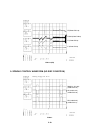
3-18 fe(ic201 pin 18) foso(ic501 pin12) f+(ic202 pin 9) f-(ic202 pin 8) fig 8-2 (cd) 9. Spindle control waveform (no disc condition) dmso(1.4v/1.8v) (ic501 pin 18) sp-(3.6v/2.4v) (ic202 pin 10) sp+(3.6v/4.8v) (ic202 pin 11) fig 9-1.
Page 37
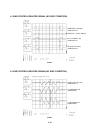
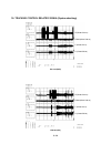
3-19 10. Tracking control related signal(system checking) te(ic201 pin 21) trso(ic501 pin 13) t-(ic202 pin 7) t+(ic202 pin 6) fig 10-1(dvd) te(ic201 pin 21) trso(ic501 pin 13) t-(ic202 pin 7) t+(ic202 pin 6) fig 10-2(cd).
Page 38
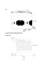
3-20 11. Rf waveform rfop(2.3v/1.1v) (ic201 pin 6) rfon(0.8v/2.0v) (ic201 pin 7) fig 11-1 12. Mt1379 audio optical and coaxial output (aspdif) (ic501 pin 153) fig 12-1.
Page 39
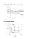
3-21 13. Mt1379 video output waveform 1) full colorbar signal(cvbs) (ic604 pin 23) dclk = 93mhz, vp-p=2.2, vmax=2.7v fig 13-1 2) y (ic604 pin 21) fig 13-2.
Page 40
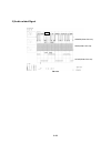
3-22 3) c (ic604 pin 26) dclk = 93mhz, vp-p=2.2, vmax=2.7v fig 13-3 14. Audio output from audio dac 1) audio l/r fig 14-1 (jk601 pin 4,5).
Page 41
3-23 2) audio related signal asdat3(ic501 pin 157) abck(ic501 pin 148) alrck(ic501 pin 149) asdata3 fig 14-2.
Page 42: Block Diagrams
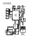
3-24 block diagrams 1. Overall block diagram m m disc spindle motor loading motor deck mechanism dvd:rf0,a,b,c,d cd:rf0,a,b,c,d,e,f pick up dig901 fld display key input 5mhz x-tal b/u ic5a1 29lv160te 2m 8bit flash rom a[00:20] pce# prd# pwr# dq[00:15] rfon,rfop,feo,rfl,cso teo,bdo,rfrp,htrc,v2p8 l/r...
Page 43
3-25 2. Power(smps) block diagram 5v_a -29va vf+ rectifier line filter switching ic trans feed b. Reg(8v) 8v 5.2va vf- rectifier(fld ) rectifier(9v) rectifier(5.2v) lpf lpf rectifier(14v) lpf 12 v ac90~240v pwr on/off reg(3.3v) 3.3v/3.3v_m reg(12v ) on/of f rectifier(3.8v) lpf loewe.
Page 44
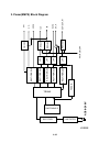
3-26 ic202 la6560 motor driver dvd: a,b,c,d, rfo cd: a,b,c,d, e, f,rfo sp+, sp - m/ d pick up x501 ic501 mt1379 dvdplayer combo chip ic201 mt1336e rf signa l processor foso,trso,fmso dmso,,tropen feo,teo,rfl,rfrp bdo,cso,htrc,v2p8 adi n f+, f-, t +, t - sl+ , sl - load+, load - 27m h z x- t a l rfop...
Page 45
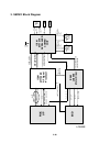
3-27 4. Mpeg & memory block diagram ic503 sdra m 16 m ic505 eepro m iic 501 (mpeg + dsp ) mt1379 ic5a 1 flash memory (16 m ) ic510 (74hct244 ) voltage level shift video int e rface audio int erface rf ic int erface front mi co m in te rfa c e (f r o n t b o a r d ) ic502 sdra m 16 m rfop,rfon,htrc,r...
Page 46
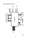
3-28 5. Video & audio block diagram ic604 video 6db amp ic401 audio dac (2ch) ic402 (op amp) lpf&buffer cvbs ) dac reset aclk scl sd a a/ v jac k mp eg mp eg audio ‘r ’ audio ‘r ’ adata3 loewe component (r.G.B) / (y.Pb.Pr super video (y/c) (r.G.B) / (y.Pb.Pr ) (y/c).
Page 47
3-41 3-42 pin stop play stop play stop play stop play stop play stop play 1 1.03 2.99 0 0 3.28 3.29 5.52 5.49 1.22 1.22 3.27 3.28 2 5.11 5.08 0 0 3.28 3.28 5.52 5.48 0 0 1.18 1.26 3 0 0 8.04 8.01 0 1.65 5.51 5.47 0.96 0.9 1.1 1.52 4 0 0 0.12 0.06 1.63 1.64 0 0 2 2.06 0 0 5 5.11 5.07 0 0.06 1.64 1.65...
Page 48
3-43 3-44 pin stop play stop play stop play stop play stop play stop play 161 0 1.27 162 0 2.35 163 0 0 164 0 0.73 165 0 3.27 166 0 0.5 167 0 0 168 0 0.53 169 0 3.27 170 0 0.59 171 0 0 172 3.01 0.72 173 0 0.72 174 0 0 175 0 2.73 176 0 3.13 177 0 3.13 178 0 3.25 179 0 0 180 0 0 181 2.04 2.64 182 0 2....

