- DL manuals
- Magnavox
- TV VCR Combo
- 19MDTR17
- Service Manual
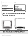
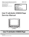
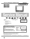
Magnavox 19MDTR17 Service Manual
Color TV with Built-In VCR/DVD Player
First Issue: 5/03
2003 Philips Consumer Electronics Company
Philips Consumer Electronics Company
A Division of Philips Electronics North America Corporation
Technical Service Data
Service Solutions Group
Technical Publications Dept.
P.O. Box 555, 401 E. Old Andrew Johnson Hwy.
Jefferson City,TN 37760
MANUAL 5891
Sec. 1A: Main Section
( 27MDTR20S/17 )
MAGNAVOX
Model: 27MDTR20S/17
Sec. 2: Deck Mechanism Section
MA
NU
AL 58
91
Color TV
w
it
h
Built
-In VCR
/D
V
D P
la
y
e
r
Ma
gna
v
o
x
27M
DTR20S
/17
, 19
MDTR2
0
/17
Color TV with Built-In VCR/DVD Player
Service Manual
MAGNAVOX
Model: 19MDTR20/17
Supplement 1
Sec. 1B: Main Section
( 19MDTR20/17 )
Specifications
Adjustment Procedures
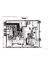
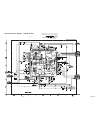
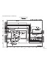
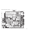
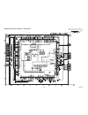
Schematic Diagrams and CBA’s
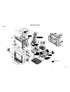
Exploded Views
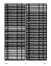
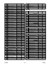
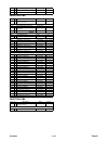
Cabinet & Electrical Parts Lists
Summary of 19MDTR17
Page 1
Color tv with built-in vcr/dvd player first issue: 5/03 2003 philips consumer electronics company philips consumer electronics company a division of philips electronics north america corporation technical service data service solutions group technical publications dept. P.O. Box 555, 401 e. Old and...
Page 2: Supplement 1
Philips consumer electronics company a division of philips electronics north america corporation technical service data service solutions group technical publications dept. P.O. Box 555, 401 e. Old andrew johnson hwy. Jefferson city,tn 37760 manual 5891 magnavox model: 19mdtr20/17 color tv with buil...
Page 3: Important Safety Notice
Important safety notice proper service and repair is important to the safe, reliable operation of all philips consumer electronics company** equipment. The service procedures recommended by philips and described in this service manual are effective methods of performing service operations. Some of t...
Page 4: Table of Contents
Table of contents note: one model, 19mdtr20/17, is covered by supplement 1. This section only shows what differs between this model and its base model covered by section 1a and the deck mechanism section. [ main section ] page specifications . . . . . . . . . . . . . . . . . . . . . . . . . . . . . ...
Page 5: Specifications
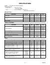
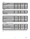
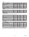
1-1-1 td851sp specifications *ˆ mode---------sp mode unless otherwise specified * test input terminal -------------video input (1vp-p) audio input (-10db) -----------------------ant. Input (80db µv) video: 87.5% audio: 25khz dev (1khz sin) description condition unit nominal limit 1. Over scan — % 90...
Page 6
1-1-2 td851sp all items are measured across 8 Ω resistor at speaker output terminal. All items are measured at tp1701 and tp1702. Note: nominal specifications represent the design specifications. All units should be able to approximate these. Some will exceed and some may drop slightly below these s...
Page 7: Preparation For Servicing
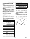
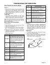
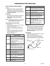
1-2-1 td857pfs preparation for servicing how to enter the service mode caution: 1 1. Optical sensors system are used for tape start and end sensor on this equipment. Read this page carefully and prepare as described on this page before starting to service; otherwise, the unit may operate unexpectedl...
Page 8
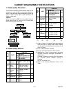
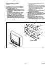
1-3-1 td857dc cabinet disassembly instructions 1. Disassembly flowchart this flowchart indicates the disassembly steps for the cabinet parts, and the cba in order to gain access to item(s) to be serviced. When reassembling, follow the steps in reverse order. Bend, route and dress the cables as they ...
Page 9
1-3-2 td857dc reference notes in the table caution ! When removing the crt, be sure to discharge the anode lead of the crt with the crt ground wire before removing the anode cap. Reference notes in the table caution 1: discharge the anode lead of the crt with the crt ground wire before removing the ...
Page 10
1-3-3 td857dc fig. 1 s-1 s-1 s-1 s-1 s-1 s-3 [1] rear cabinet s-2 fig. 2 s-1 s-1 s-2 s-3 s-1 s-1 s-1 s-1 [1] rear cabinet.
Page 11
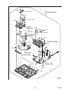
1-3-4 td857dc fig. 3 s-5 s-5 s-5 [5] shield box [2] h.V. Cba (wih holder) h.V. Cba [6] dvd mechanism [11] main cba [8] power supply/ av cba [9] function cba s-6 s-6 s-6 s-8 s-9 s-9 s-8 s-8 [10] deck assembly s-10 s-10 s-10 s-12 s-11 s-11 [3] tray chassis unit.
Page 12
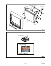
1-3-5 td857dc fig. 4 s-4 s-4 s-4 s-4 [4] crt anode cap crt cba fig. 5 a view for a pickup unit b short the three short lands by soldering view for b slide s-7 cn201 [7] dvd main cba unit dvd mechanism s-7 cn301.
Page 13
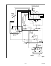
1-3-6 td857dc fig. 6 function cba ac cord cl504a cl501 screen cn501 focus anode crt gnd cn601 cn401 factory use only dvd main cba fe head cylinder assembly ac head assembly capstan motor deck assembly cn571 cl502a cl503a cl501a h.V. Cba tuner cn1802 cl1201 cn1301 cn1803 cn1804 cn1805 cl1402 cl1401 c...
Page 14
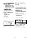
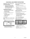
1-4-1 td857ea electrical adjustment instructions general note: "cba" is abbreviation for "circuit board assembly." note: electrical adjustments are required after replacing circuit components and certain mechanical parts. It is important to perform these adjustments only after all repairs and replac...
Page 15
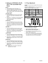
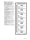
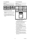
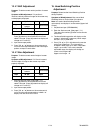
1-4-2 td857ea 2. H adjustment purpose: to get correct horizontal position and size of screen image. Symptom of misadjustment: horizontal position and size of screen image may not be properly displayed. Note: r583 --- h.V. Cba 1. Connect frequency counter to r583. 2. Operate the unit for at least 20 ...
Page 16
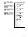
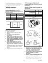
1-4-3 td857ea 5. V. Shift adjustment purpose: to obtain correct vertical position of screen image. Symptom of misadjustment: if v. Shift is incorrect, vertical position of image on the screen may not be properly displayed. 1. Enter the service mode. (see page 1-4-1.) press "9" button on the service ...
Page 17
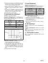
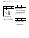
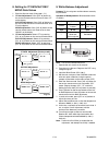
1-4-4 td857ea 12.Set the color analyzer to the chroma mode and after zero point calibration, bring the optical recep- tor to the center on the tube surface (crt). 13.Adjust the red drive as needed with the ch o / p buttons to get the following value, x= 286, y= 294. 14.Choose cut off/drive mode then...
Page 18
1-4-5 td857ea 12. Head switching position adjustment purpose: determine the head switching point during playback. Symptom of misadjustment: may cause head switching noise or vertical jitter in the picture. Note: unit reads head switching position automati- cally and displays it on the screen (upper ...
Page 19
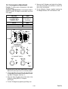
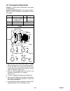
1-4-6 td857ea 14. Convergence adjustment purpose: to obtain proper convergence of red, green and blue beams. Symptom of misadjustment: if convergence adjust- ment is incorrect, the edge of white letters may have color edges. 1. Set the unit to the aux mode which is located before ch2, then input a d...
Page 20
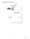
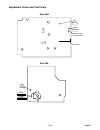
1-4-7 td857ea adjustment points and test points h.V. Cba r583 h adj. J553 +b upper focus vr lower screen vr power supply/av cba vr2601 +b adj.
Page 21
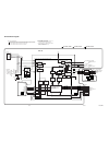
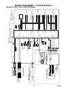
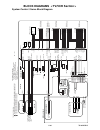
Control head cl1402 ac head assembly main cba power supply / av cba rf-sw t-reel dv-sync c-sync c-sync v-env ctl(+) d1224 s-led d1204 rec d1216 dvd d1217 tv/vcr q1210 q1211 q1207 p-on+5v rec-led key0 rs1201 remote sensor key1 dvd-h tv/vcr-led reset rota d-rec-h d-rec-h rec-safety a-mute scl remote s...
Page 22
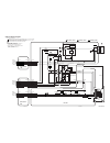
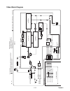
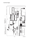
Video block diagram 1-5-3 1-5-4 td857blv rec video signal pb video signal mode: sp/rec luminance signal process main cba cl1401 q1401 tp1402 v-out v-agc r p fbc y/c mix ccd 1h delay r p doc ynr y/c comb chrominance signal process ic1401 video/audio signal process 35 42 38 17 chara mix 6db amp vxo en...
Page 23
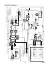
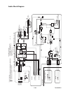
Audio block diagram block diagram for section 2 (deck mechanism) main cba power supply / av cba pb-audio signal dvd audio signal rec-audio signal 1-5-5 ic1401 td857bla 1-5-6 bias osc q1872 p-on+5v p-on+5v q1871 q1873 q1874 q1875 (audio process) n-a-in n-a-out tp1802 na-in-yca audio head ac head asse...
Page 24
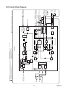
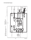
57 7 48 47 13 14 69 6 7 r-ch insel l-ch insel nor sw serial data decoder output select vco lpf l-ch bpf r-ch pnr pilot det cont stereo pll stereo filter sap filter sap det sif demod sap demod l-r demod st/sap sw matrix l-ch pnr lim dev comp sw noise vco lpf lim dev comp comp dc sw noise dbx dec env ...
Page 25
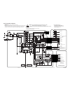
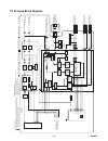
Td857blc x1301 3.58mhz cn1301 ic1301 (video/audio/chroma/deflection) sda scl fsc 10 9 13 16 ic1201 (osd) v-sync h-sync osd-r osd-g osd-b 59 58 60 62 63 64 osd-blk ext-v-in from video block v-out from/to crt/h.V. Block cn503 12 green 11 blue fbp 3 h-drive 4 acl/abl v-drive 8 v-ramp-fb chroma block di...
Page 26
Pulse up amp thermal protection 3 6 7 1 5 v-drive 8 h-drive 4 8 10 7 9 6 green amp blue amp q501 q502 q503 h.Drive q572 q571 t572 td857blcrt fbp acl/abl crt/h.V. Block diagram v- drive h- drive d.Y. L551 ic551 (v-deflection control) t571 f.B.T. Anode focus screen 3 5 cl503a 7 h.V. Cba crt cba cl504a...
Page 27
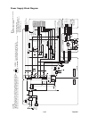
Power supply block diagram line filter bridge rectifier t2601 ic2601 error voltage det w2601 f2601 4a/125v l2601 d2603 d2606 td857blp degaussing coil cn2601 ps2601 hot cold 1-5-14 1-5-13 power supply/av cba main cba dvd main cba unit note : the voltage for parts in hot circuit is measured using hot ...
Page 28
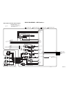
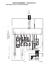
Dvd system control/servo block diagram td857blds 27 7 8 3 15 10 14 26 1 2 3 4 6 23 5 17 18 12 11 14 13 15 16 25 24 54 cs 55 sdata 61 remote pwrcon pwrcon 53 sclk cn401 dvd main cba unit drive cba ic301 (servo drive) ic451 (clock generator) block diagrams ic202 (op amp) 12 14 cn301 fg cba fg sensor m...
Page 29
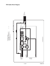
Digital signal process block diagram td857bld c 6 d 7 a 8 b 5 f 10 e 2 dvd-ld 14 cd-ld 12 pd-moni 13 fs(+) 18 fs(-) 19 ts(+) 20 ts(-) 17 cn201 cn201 cn201 ic201 (sw) ic105 (latch) ic102 (sdram) ic101 (micro controller) fs fs(+) cd/dvd fs(-) ts(+) ts(-) ts pick-up unit detector cd/dvd 9 q251,q252 cd ...
Page 30
Dvd audio block diagram td857blad ic601 (audio dac) 7 8 cn601 1 2 3 13 14 15 16 from dvd system control /servo block from digital signal process block serial port serial control 4x/8x oversampling digital filter /function controller enhanced multi-level delta-sigma modulator dac lpf+amp l-ch r-ch lp...
Page 31
1-6-1 sc_5 2 3 1 5.0 (2.5) play mode stop mode 5.0 the same voltage for both play & stop modes indicates that the voltage is not consistent here. 2 3 1 5.0 (2.5) [ ] 5.0 indicates that the voltage is not consistent here. Tv/vcr section > unit: volts play mode rec mode dvd mode the same voltage for p...
Page 32
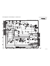
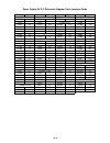
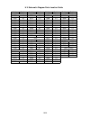
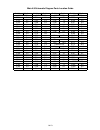
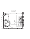
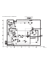
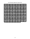
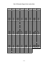
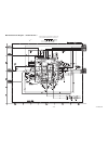
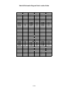
1-6-2 main 1/5 schematic diagram parts location guide ref no. Position ref no. Position ref no. Position ref no. Position c1207 a-1 d1207 a-1 r1214 a-4 r1259 d-1 c1208 a-1 d1208 b-1 r1215 a-4 r1260 d-1 c1209 b-1 d1210 d-1 r1216 a-4 r1262 d-3 c1210 b-1 d1213 c-4 r1217 a-4 r1263 d-3 c1211 b-1 d1216 a-...
Page 33
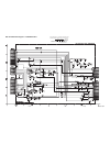
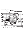
Main 1/5 schematic diagram 1-6-3 1-6-4 td857scm1 voltage indications for play, rec and dvd modes on the schematic diagrams are as shown below: 1 2 3 5.0 (2.5) 0 > ~ 5.0 the same voltage for play,rec & dvd modes. Indicates that the voltage is not consistent here. Play mode rec mode dvd mode.
Page 34
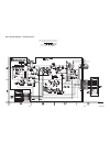
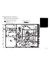
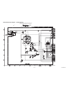
1-6-5 1-6-6 td857scm2 main 2/5 schematic diagram voltage indications for play, rec and dvd modes on the schematic diagrams are as shown below: 1 2 3 5.0 (2.5) 0 > ~ 5.0 the same voltage for play,rec & dvd modes. Indicates that the voltage is not consistent here. Play mode rec mode dvd mode.
Page 35
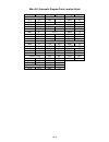
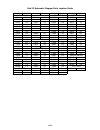
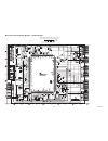
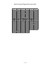
1-6-7 main 2/5 schematic diagram parts location guide ref no. Position ref no. Position ref no. Position ref no. Position c1410 i-2 c1445 g-3 q1401 k-2 r1435 h-3 c1411 j-2 c1446 h-3 q1402 k-3 r1853 h-4 c1412 j-2 c1447 g-3 q1403 k-4 r1856 h-4 c1413 j-2 c1449 k-2 q1871 g-2 r1857 h-4 c1414 j-2 c1452 k-...
Page 36
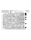
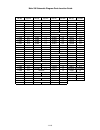
Main 3/5 schematic diagram parts location guide 1-6-8 ref no. Position ref no. Position ref no. Position ref no. Position c1002 p-1 c1333 n-1 d1352 q-3 r1311 n-4 c1003 p-1 c1336 o-2 r1312 o-4 c1005 q-1 c1337 o-2 ic1301 n-2 r1314 n-4 c1006 p-1 c1338 o-2 r1315 n-4 c1007 q-1 c1339 o-2 l1001 p-1 r1316 n...
Page 37
1-6-9 1-6-10 td857scm3 main 3/5 schematic diagram voltage indications for play, rec and dvd modes on the schematic diagrams are as shown below: 1 2 3 5.0 (2.5) 0 > ~ 5.0 the same voltage for play,rec & dvd modes. Indicates that the voltage is not consistent here. Play mode rec mode dvd mode.
Page 38
1-6-11 1-6-12 td857scm4 main 4/5 schematic diagram voltage indications for play, rec and dvd modes on the schematic diagrams are as shown below: 1 2 3 5.0 (2.5) 0 > ~ 5.0 the same voltage for play,rec & dvd modes. Indicates that the voltage is not consistent here. Play mode rec mode dvd mode.
Page 39
Main 4/5 schematic diagram parts location guide 1-6-13 ref no. Position ref no. Position ref no. Position ref no. Position c1722 v-1 c1769 v-4 c1793 t-2 r1756 v-2 c1732 v-1 c1770 v-4 c1794 v-2 r1757 t-3 c1747 v-3 c1771 v-4 c1795 t-2 r1758 t-3 c1748 u-4 c1772 u-4 c1797 t-4 r1759 t-2 c1749 s-4 c1773 u...
Page 40
Main 5/5 schematic diagram parts location guide 1-6-14 ref no. Position ref no. Position ref no. Position ref no. Position c1419 y-3 c1825 y-4 l1804 bb-1 r1805 aa-2 c1627 y-2 c1826 z-4 l1806 bb-1 r1806 aa-1 c1628 y-2 l1807 bb-1 r1807 aa-1 c1629 y-2 cn1802 bb-1 r1808 aa-1 c1631 x-2 cn1803 x-2 q1608 y...
Page 41
1-6-15 1-6-16 td857scm5 main 5/5 schematic diagram voltage indications for play, rec and dvd modes on the schematic diagrams are as shown below: 1 2 3 5.0 (2.5) 0 > ~ 5.0 the same voltage for play,rec & dvd modes. Indicates that the voltage is not consistent here. Play mode rec mode dvd mode.
Page 42
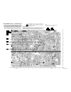
Main cba parts location guide 1-6-17 1-6-18 ref no. Position ref no. Position ref no. Position ref no. Position ref no. Position ref no. Position c1002 a-5 c1327 a-4 c1634 a-1 c1800 c-2 d1231 d-5 q1205 f-2 c1003 a-5 c1330 a-4 c1635 a-1 c1802 b-3 d1302 b-5 q1206 e-3 c1005 a-5 c1331 a-4 c1636 e-2 c180...
Page 43
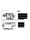
Ctl-amp-out tp1201 wf3 na-in-yca tp1802 wf7 rf-sw tp1401 wf1 v-out tp1402 wf5 gnd tp1632 ha-monitor tp1403 wf6 main cba top view 1-6-19 btd850f01011 1-6-20 bhb300f01014-a bhb300f01014-b sensor cba top view.
Page 44
Pin 58 of ic1201 pin 59 of ic1201 pin 61 of ic1401 pin 42 of ic1401 pin 7 of ic1401 pin 41 of ic1301 wf8 wf4 wf16 wf15 wf2 wf9 main cba bottom view 1-6-21 1-6-22 btd850f01011.
Page 45
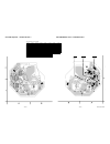
2 +b adj vr2601 dvd-c tp2204 wf18 dvd-y tp2203 wf18 power supply / av cba top view 1-6-23 1-6-24 btd850f01021a because a hot chassis ground is present in the power supply circuit, an isolation transformer must be used. Also, in order to have the ability to increase the input slowly, when troubleshoo...
Page 46
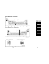
Power supply / av cba bottom view 1-6-25 1-6-26 btd850f01021a because a hot chassis ground is present in the power supply circuit, an isolation transformer must be used. Also, in order to have the ability to increase the input slowly, when troubleshooting this type power supply circuit, a variable i...
Page 47
Power supply / av cba parts location guide 1-6-27 1-6-28 ref no. Position ref no. Position ref no. Position ref no. Position ref no. Position ref no. Position c2217 d-2 c2616 a-3 d2245 d-2 d2646 b-3 q2207 d-2 r2233 d-2 c2218 d-2 c2617 a-3 d2412 d-2 d2648 c-4 q2210 d-1 r2236 d-2 c2222 a-1 c2618 b-3 d...
Page 48
1-6-29 1-6-30 power supply /av 1/2 schematic diagram parts location guide ref no. Position ref no. Position ref no. Position ref no. Position ref no. Position ref no. Position c2401 d-3 c2651 b-2 d2628 d-3 q2607 e-1 r2629 c-2 r2665 d-3 c2604 c-2 c2661 e-3 d2631 a-4 q2608 d-3 r2630 c-2 r2666 d-3 c260...
Page 49
Note : the voltage for parts in hot circuit is measured using hot gnd as a common terminal. Caution: for continued protection against risk of fire, replace only with same type 4a, 125v fuse. Attention: utiliser un fusible de rechange de mÊme type de 4a, 125v. 4a/125v caution ! Fixed voltage ( or aut...
Page 50
Power supply/av 2/2 schematic diagram 1-6-33 1-6-34 td857scp2 voltage indications for play, rec and dvd modes on the schematic diagrams are as shown below: 1 2 3 5.0 (2.5) 0 > ~ 5.0 the same voltage for play,rec & dvd modes. Indicates that the voltage is not consistent here. Play mode rec mode dvd m...
Page 51
Power supply/av 2/2 schematic diagram parts location guide 1-6-35 ref no. Position ref no. Position ref no. Position ref no. Position c2217 i-2 d2206 i-4 q2623 h-2 r2302 h-3 c2218 i-2 d2245 i-3 r2303 h-3 c2222 k-4 d2412 k-2 r2202 h-4 r2304 i-3 c2224 k-4 d2413 k-1 r2203 h-4 r2305 i-3 c2225 h-4 d2661 ...
Page 52
1-6-36 h.V. Schematic diagram parts location guide ref no. Position ref no. Position ref no. Position ref no. Position c552 a-2 d571 b-2 r559 a-2 r587 c-1 c553 a-1 d572 c-2 r560 a-1 r588 c-1 c555 a-2 d584 c-2 r561 a-1 r589 b-2 c556 a-1 d585 c-2 r562 a-1 r590 b-2 c558 a-2 d591 b-1 r563 a-1 r591 b-1 c...
Page 53
1-6-37 td857schv h.V. Schematic diagram 1-6-38 voltage indications for play, rec and dvd modes on the schematic diagrams are as shown below: 1 2 3 5.0 (2.5) 0 > ~ 5.0 the same voltage for play,rec & dvd modes. Indicates that the voltage is not consistent here. Play mode rec mode dvd mode.
Page 54
1-6-39 1-6-40 h.V. Cba parts location guide junction-a cba top view junction-a cba bottom view junction-b cba top view junction-b cba bottom view btd850f01031-c btd850f01031-d ref no. Position ref no. Position ref no. Position c552 b-2 d597 c-2 r574 c-1 c553 c-2 d598 c-2 r575 c-1 c555 b-2 r576 c-1 c...
Page 55
Focus-vr (upper side) screen-vr (lower side) +b adj j553 r583 (h adjustment) gnd j563 h.V. Cba top view 1-6-41 1-6-42 btd850f01031-a.
Page 56
Wf11 pin 5 of cn571 q571 collector wf10 1-6-43 1-6-44 h.V. Cba bottom view btd850f01031-a.
Page 57
1-6-46 td857sccrt crt schematic diagram td857scf function schematic diagram 1-6-45 voltage indications for play, rec and dvd modes on the schematic diagrams are as shown below: 1 2 3 5.0 (2.5) 0 > ~ 5.0 the same voltage for play,rec & dvd modes. Indicates that the voltage is not consistent here. Pla...
Page 58
Wf12 q501 collector wf13 q502 collector wf14 q503 collector 1-6-47 1-6-48 btd850f01031-b crt cba top view crt cba bottom view crt cba parts location guide ref no. Position ref no. Position ref no. Position ref no. Position c501 a-1 q501 a-2 r507 b-2 r520 a-2 c502 a-2 q502 a-2 r508 a-2 r521 a-2 c503 ...
Page 59
1-6-49 btd850f01021b 1-6-50 function cba top view function cba bottom view ref no. Position cn2801 a-2 cn2805 d-1 l2401 a-1 l2402 a-2 r2401 d-1 r2402 d-1 r2403 c-1 r2404 c-1 r2405 c-1 r2406 c-1 r2407 c-1 sw2401 d-1 sw2402 d-1 sw2403 d-1 sw2404 c-1 sw2405 c-1 sw2406 c-1 sw2407 b-1 sw2408 b-1 function...
Page 60
1-6-51 1-6-52 td857scd1 dvd main 1/3 schematic diagram voltage indications for play and stop modes on the schematic diagrams are as shown below: 1 2 3 5.0 (2.5) ~ 5.0 the same voltage for both play & stop modes. Indicates that the voltage is not consistent here. Play mode stop mode “ “ = smd.
Page 61
1-6-53 1-6-54 td857scd2 dvd main 2/3 schematic diagram voltage indications for play and stop modes on the schematic diagrams are as shown below: 1 2 3 5.0 (2.5) ~ 5.0 the same voltage for both play & stop modes. Indicates that the voltage is not consistent here. Play mode stop mode “ “ = smd.
Page 62
1-6-55 1-6-56 ic101 voltage chart pin.No play stop pin.No play stop pin.No play stop pin.No play stop pin.No play stop 1 3.3 3.3 33 2.2 2.9 65 0.1 0.1 97 3.4 3.4 129 2.0 2.0 2 ~ ~ 34 ~ ~ 66 1.2 2.5 98 1.6 1.6 130 2.2 2.2 3 ~ ~ 35 ~ ~ 67 1.6 1.6 99 0 0 131 2.3 2.3 4 0 0 36 ~ ~ 68 3.4 3.4 100 ----- --...
Page 63
1-6-57 1-6-58 td857scd3 dvd main 3/3 schematic diagram voltage indications for play and stop modes on the schematic diagrams are as shown below: 1 2 3 5.0 (2.5) ~ 5.0 the same voltage for both play & stop modes. Indicates that the voltage is not consistent here. Play mode stop mode “ “ = smd.
Page 64
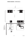
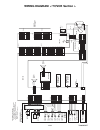
Wiring diagram 1-7-1 td857wit 1-7-2 crt cba btd850f01031-b h.V. Cba btd850f01031-a focus screen gnd l551 d.Y. Hd vd cl501a cl501 cl503a main cba btd850f01011 power supply /av cba btd850f01021a function cba btd850f01021b cn1301 cn501 w2601 1 2 3 4 5 t571 fbt cl504a anode 1 2 3 4 5 1 2 3 4 9 10 11 12 ...
Page 65
Dvd mecha 1-7-3 1-7-4 wiring diagram dvd main cba unit td857wid pick up unit cn201 cn301 1 2 3 4 tray-out tray-in gnd 5 6 sp(-) 7 sp(+) 8 sl(-) 9 sl(+) fg-in dvd-on+3.3v tray-in cn401 cn601 drive cba fs ts detector 11 2 3 5 6 4 7 fg cba fg sensor tray-out sw3001 sw3002 m sled motor m spindle motor 1...
Page 66
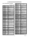
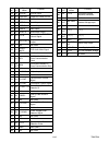
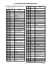
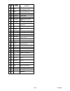
1-8-1 td857pin ic pin function descriptions ic1201 (tv/vcr micro computer) “h” ≥ 4.5v, “l” ≤ 1.0v pin no. In/ out signal name function 1 in ld-sw loading switch input 2 in p-safety 1 power supply failure detection 1 3 in p-safety 2 power supply failure detection 2 4 in st/sap-in tuner stereo/sap det...
Page 67
1-8-2 td857pin 59 in v-sync v-sync input 60 out osd-blk output for picture cut off 61 - nu not used 62 out osd-b blue output 63 out osd-g green output 64 out osd-r red output 65 out a-mute audio mute output 66 out c-f/r capstan motor fwd/rev control signal 67 out jack-mute earphone jack audio mute o...
Page 68: Lead Identifications
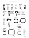
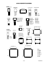
1-9-1 td857le 2sc3331(t,u) 2sc1627y-tpe2 2sa950(y,o) kta1271(y) 2sc3400 2sa1175(f) kta1267(gr) krc103m ktc3199(gr) 2sc2785(j,h,f) ba1f4m-t bn1f4m-t kra103m 2sd400(f) 2sc2482 tpe6 2sc3468(e,d)-ae e c b e c b 2sc1815-gr(tpe2) 2sc2120-(o,y)(tpe2) kta1266(gr) ktc3198(gr) 2sa1015-gr(tpe2) kia7805api ka78...
Page 69: Electrical Parts List
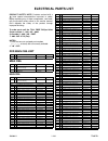
20030411 1-10-1 td857el electrical parts list product safety note: products marked with a # have special characteristics important to safety. Before replacing any of these components, read care- fully the product safety notice in this service manual. Don't degrade the safety of the product through i...
Page 70
20030411 1-10-2 td857el c1332 electrolytic cap. 1µf/50v ±20% or ce1jmasdl1r0 4835 124 47305 electrolytic cap. 1µf/50v ±20% or ce1jmasdl010 4835 124 47014 electrolytic cap. 1µf/50v ±20% ce1jmastl1r0 4835 124 47014 c1333 electrolytic cap. 1µf/50v ±20% or ce1jmasdl1r0 4835 124 47305 electrolytic cap. 1...
Page 71
20030411 1-10-3 td857el c1777 electrolytic cap. 1µf/50v ±20% or ce1jmasdl1r0 4835 124 47305 electrolytic cap. 1µf/50v ±20% or ce1jmasdl010 4835 124 47014 electrolytic cap. 1µf/50v ±20% ce1jmastl1r0 4835 124 47014 c1778 ceramic cap.(ax) 0.01µf/50v ±10% (b) cca1jkt0b103 ---- --- ----- c1779 electrolyt...
Page 72
20030411 1-10-4 td857el d1219 zener diode mtzjt-776.2b or qdtb0mtzj6r2 4835 130 37593 zener diode dz-6.2bsbt265 ndtb0dz6r2bs 4835 130 38039 d1224 led sir-563st3f p or qpqps1r563st 4835 130 87163 led sir-563st3f q qpqqs1r563st 4835 130 87162 d1227 pcb jumper d0.6-p5.0 jw5.0t ---- --- ----- d1229 zene...
Page 73
20030411 1-10-5 td857el tv/vcr led drive ktc3198(gr) "npn" or nqs40ktc3198 4835 130 47946 tv/vcr led drive 2sc1815-gr(tpe2) "npn" qqs102sc1815 4835 130 47358 q1211 dvd led drive 2sc2785(f) "npn" or qqsf02sc2785 4835 130 47722 dvd led drive 2sc2785(h) "npn" or qqsh02sc2785 4835 130 47722 dvd led driv...
Page 74
20030411 1-10-6 td857el r1216 carbon res. 1/4w 1.5k Ω ±2% or rcx4gatz0152 4835 110 57186 carbon res. 1/6w 1.5k Ω ±2% rcx6gatz0152 4835 111 37306 r1217 carbon res. 1/4w 2.2k Ω ±2% or rcx4gatz0222 4835 110 57079 carbon res. 1/6w 2.2k Ω ±2% rcx6gatz0222 4835 111 37176 r1218 carbon res. 1/4w 2.7k Ω ±2% ...
Page 75
20030411 1-10-7 td857el carbon res. 1/6w 100 Ω ±5% rcx6jatz0101 4835 111 37161 r1332 carbon res. 1/4w 22 Ω ±5% or rcx4jatz0220 4835 110 57036 carbon res. 1/6w 22 Ω ±5% rcx6jatz0220 4835 111 37174 r1333 carbon res. 1/4w 100 Ω ±5% or rcx4jatz0101 4835 110 57003 carbon res. 1/6w 100 Ω ±5% rcx6jatz0101 ...
Page 76
20030411 1-10-8 td857el r1808 carbon res. 1/4w 33k Ω ±5% or rcx4jatz0333 4835 110 57211 carbon res. 1/6w 33k Ω ±5% rcx6jatz0333 4835 110 57211 r1809 carbon res. 1/4w 33k Ω ±5% or rcx4jatz0333 4835 110 57211 carbon res. 1/6w 33k Ω ±5% rcx6jatz0333 4835 110 57211 r1814 # metal oxide film res. 2w 3.9 Ω...
Page 77
20030411 1-10-9 td857el sensor cba h.V. Cba assembly h.V. Cba tb7 led holder td851ub 0em408042 ---- --- ----- tb13 bush, led(f) h3700ud 0vm409508 ---- --- ----- tp1201 pcb jumper d0.6-p10.0 jw10.0t ---- --- ----- tp1401 pcb jumper d0.6-p22.5 jw22.5t ---- --- ----- tp1402 pcb jumper d0.6-p15.0 jw15.0...
Page 78
20030411 1-10-10 td857el crt cba resistors r519 carbon res. 1/4w 56k Ω ±5% or rcx4jatz0563 4835 110 57213 carbon res. 1/6w 56k Ω ±5% rcx6jatz0563 4835 111 37201 r520 carbon res. 1/4w 56k Ω ±5% or rcx4jatz0563 4835 110 57213 carbon res. 1/6w 56k Ω ±5% rcx6jatz0563 4835 111 37201 r521 carbon res. 1/4w...
Page 79
20030411 1-10-11 td857el junction a cba junction b cba mps cba power supply/av cba r508 carbon res. 1/4w 1.5k Ω ±5% rcx4jatz0152 4835 110 57186 r509 carbon res. 1/4w 1.5k Ω ±5% rcx4jatz0152 4835 110 57186 r513 carbon res. 1/4w 15 Ω ±5% or rcx4jatz0150 4835 110 57177 carbon res. 1/6w 15 Ω ±5% rcx6jat...
Page 80
20030411 1-10-12 td857el electrolytic cap. 10µf/50v ±20% ce1jmastl100 4835 124 47037 c2630 # safety cap. 4700pf/250v kx ca2e472mr050 4835 124 17078 c2631 electrolytic cap. 1000µf/6.3v ±20% or ce0kmasdl102 4835 124 47203 electrolytic cap. 1000µf/6.3v ±20% ce0kmastl102 4835 124 47203 c2632 electrolyti...
Page 81
20030411 1-10-13 td857el l2203 pcb jumper d0.6-p5.0 jw5.0t ---- --- ----- l2204 pcb jumper d0.6-p5.0 jw5.0t ---- --- ----- l2205 pcb jumper d0.6-p5.0 jw5.0t ---- --- ----- l2206 pcb jumper d0.6-p5.0 jw5.0t ---- --- ----- l2401 pcb jumper d0.6-p5.0 jw5.0t ---- --- ----- l2402 pcb jumper d0.6-p5.0 jw5...
Page 82
20030411 1-10-14 td857el inverter 2sc2785(j) "npn" or qqsj02sc2785 4835 130 47722 inverter ktc3199(gr) "npn" or nqs10ktc3199 4835 130 47914 inverter ktc3198(gr) "npn" or nqs40ktc3198 4835 130 47946 inverter 2sc1815-gr(tpe2) "npn" qqs102sc1815 4835 130 47358 q2622 inverter 2sc2785(f) "npn" or qqsf02s...
Page 83
20030411 1-10-15 td857el r2631 carbon res. 1/4w 12k Ω ±5% or rcx4jatz0123 4835 110 57282 carbon res. 1/6w 12k Ω ±5% rcx6jatz0123 4835 111 37166 r2632 # carbon res. 1/4w 680 Ω ±5% or rcx4jatz0681 4835 110 57054 # carbon res. 1/6w 680 Ω ±5% rcx6jatz0681 4835 111 37203 r2633 # carbon res. 1/4w 5.6k Ω ±...
Page 84
20030411 1-10-16 td857el function cba t2601 # switching trans 03703 ltt00cpkt108 4835 148 87438 tb9 x3 filter heat sink pgl td500ua 0em407094 ---- --- ----- tb17 x3 pow heat sink pgk assemblytd500ua 0em407108 ---- --- ----- tl2 screw, b-tight m3x8 bind head+ gbmb3080 ---- --- ----- tl6 screw, b-tigh...
Page 85
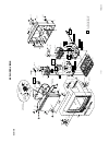
A1x cln551 v501 sp2801 cl2801 dl2 dl2 db2 dl1 dl1 db1 tl1 tl1 tl1 tl1 tb1 tl6 tl2 1b1 tb17 tb24 tb9 tl1 tl14 tl18 tl1 tl1 tl1 tb7 tb10 tb13 tb3 tl1 tl1 tl1 tl1 b3 tb2 tb23 tl3 tl3 tb14 tl5 see electrical parts list for parts with this mark. Crt cba scotch tape #880 scotch tape #880 v501-1 l551 detai...
Page 86
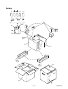
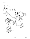
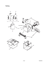
1-11-3 td857pex s2 packing tape s6 s7 s1 s3 s4 s4 x1 x12 x3 x4 x9 s4 tape x13 x25 x2 x11 x8 x10 packing.
Page 87: Mechanical Parts List
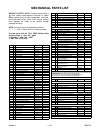
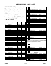
20030411 1-12-1 td857ca mechanical parts list product safety note: products marked with a # have special characteristics important to safety. Before replacing any of these components, read care- fully the product safety notice in this service manual. Don't degrade the safety of the product through i...
Page 88
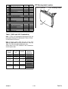
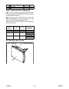
20030411 1-12-2 td857ca table 1 (v501 and l551 combination) note 1: purity and convergence adjustments must be performed following crt replacement. Refer to electri- cal adjustment instructions. Note 2: please confirm crt type no. On the crt warning label which is located on the crt. Then see table ...
Page 89
Philips consumer electronics company a division of philips electronics north america corporation service solutions group philips consumer electronics company service solutions group technical publications dept. P.O. Box 555, 401 e. Old andrew johnson hwy. Jefferson city,tn 37760
Page 90: Second Generation
Color tv with built-in vcr/dvd player first issue: 6/04 2004 philips consumer electronics company philips consumer electronics company a division of philips electronics north america corporation technical service data service solutions group technical publications dept. P.O. Box 555, 401 e. Old and...
Page 91: Supplement 2
Philips consumer electronics company a division of philips electronics north america corporation technical service data service solutions group technical publications dept. P.O. Box 555, 401 e. Old andrew johnson hwy. Jefferson city,tn 37760 manual 5899 color tv with built-in vcr/dvd player first is...
Page 92: Important Safety Notice
Important safety notice proper service and repair is important to the safe, reliable operation of all philips consumer electronics company** equipment. The service procedures recommended by philips and described in this service manual are effective methods of performing service operations. Some of t...
Page 93: Table of Contents
Table of contents note: one model, 19mdtr20/17, is covered by supplement 2. This section only shows what differs between this model and its base model, covered by section 1a and deck mechanism section. [ main section ] page specifications . . . . . . . . . . . . . . . . . . . . . . . . . . . . . . ....
Page 94: Specifications
1-1-1 t0001sp specifications *ˆ mode---------sp mode unless otherwise specified * test input terminal -------------video input (1vp-p) audio input (-10db) -----------------------ant. Input (80db µv) video: 87.5% audio: 25khz dev (1khz sin) description condition unit nominal limit 1. Over scan — % 90...
Page 95
1-1-2 t0001sp all items are measured across 8 Ω resistor at speaker output terminal. Note: nominal specifications represent the design specifications. All units should be able to approximate these. Some will exceed and some may drop slightly below these specifications. Limit specifications represent...
Page 96: Preparation For Servicing
1-2-1 t0006pfs preparation for servicing how to enter the service mode caution: 1 1. Optical sensors system are used for tape start and end sensor on this equipment. Read this page carefully and prepare as described on this page before starting to service; otherwise, the unit may operate unexpectedl...
Page 97
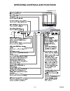
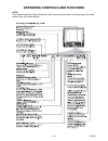
1-3-1 t0006ib operating controls and functions *27mdtr20/17 view.
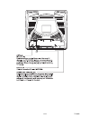
Page 98
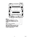
1-3-2 t0006ib *27mdtr20/17 view.
Page 99: Remote Control Operation
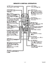
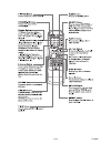
1-4-1 t0006ibr remote control operation.
Page 100
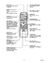
1-4-2 t0006ibr.
Page 101
1-5-1 t0006dc cabinet disassembly instructions 1. Disassembly flowchart this flowchart indicates the disassembly steps for the cabinet parts, and the cba in order to gain access to item(s) to be serviced. When reassembling, follow the steps in reverse order. Bend, route and dress the cables as they ...
Page 102
1-5-2 t0006dc reference notes in the table caution ! When removing the crt, be sure to discharge the anode lead of the crt with the crt ground wire before removing the anode cap. Reference notes in the table caution 1: discharge the anode lead of the crt with the crt ground wire before removing the ...
Page 103
1-5-3 t0006dc fig. 2 (s-6) (s-8) (s-7) loader shield top [5] dvd main cba unit loader shield bottom [6] dvd mechanism [4] dvd unit [2] tray chassis unit (s-9) (s-5) (s-10) (s-13) (s-13) top shield (s-14) (s-14) (s-14) (s-11) (s-11) (s-11) (s-11) [7] sub cba (s-12) (s-12) [8] function cba [9] deck as...
Page 104
1-5-4 t0006dc fig. 3 [3] crt anode cap crt cba (s-4) (s-4) (s-4) (s-4) a short the three short lands by soldering. (either of two places.) connector view for a fig. 4 dvd mechanism.
Page 105
1-5-5 t0006dc anode crt gnd cn601 cn401 factory use only dvd main cba fe head cylinder assembly ace head assembly capstan motor deck assembly tuner main cba sub cba crt cba to speaker to speaker cl504a screen cl501b cn501a focus cn802 cl201 cn602 cn301 cn302 cn803 cl402 cn601 cl401 cl403 cl501a cn57...
Page 106
1-6-1 t0006ea electrical adjustment instructions general note: "cba" is abbreviation for "circuit board assembly." note: electrical adjustments are required after replacing circuit components and certain mechanical parts. It is important to perform these adjustments only after all repairs and replac...
Page 107
1-6-2 t0006ea 2. Setting for contrast, color, tint and v-tint data values general 1. Enter the service mode. (see page 1-6-1.) 2. Press "picture" button on the service remote con- trol unit. Display changes "brt," "cnt," "col," "tnt," and "v-tnt" cyclically when "picture" but- ton is pressed. Contra...
Page 108
1-6-3 t0006ea 3-2. Setting for y dl time tv, y dl time ext, y sw lpf, black stretch off, black stretch cont and c. Angle data values 1. Enter the service mode. (see page 1-6-1.) 2. Y dl time tv adjustment: press "0" button on the service remote control unit twice to show "d-t tv" on the display. Y d...
Page 109
1-6-4 t0006ea 4. Setting for cd-vol, dvd-brt and dvd-sharp data values 1. Enter the service mode. (see page 1-6-1.) 2. Cd-vol adjustment: press "vol o" button on the service remote control unit once to show "cd vol" on the display. Dvd-brt adjustment: press "vol o" button on the service remote contr...
Page 110
1-6-5 t0006ea 5. H fo adjustment purpose: to get correct horizontal position and size of screen image. Symptom of misadjustment: horizontal position and size of screen image may not be properly displayed. Note: r583 --- sub cba 1. Connect frequency counter to r583. 2. Operate the unit for at least 2...
Page 111
1-6-6 t0006ea 7. White balance adjustment purpose: to mix red, green and blue beams correctly for pure white. Symptom of misadjustment: white becomes bluish or reddish. Note: use service remote control unit 1. Operate the unit more than 20 minutes. 2. Face the unit to the east. Degauss the crt using...
Page 112
1-6-7 t0006ea 9. Focus adjustment purpose: set the optimum focus. Symptom of misadjustment: if focus adjustment is incorrect, blurred images are shown on the display. Note: focus vr --- fbt (sub cba), fbt= fly back transformer 1. Operate the unit more than 30 minutes. 2. Face the unit to the east an...
Page 113
1-6-8 t0006ea 13. Head switching position adjustment purpose: determine the head switching position dur- ing playback. Symptom of misadjustment: may cause head switching noise or vertical jitter in the picture. Note: unit reads head switching position automati- cally and displays it on the screen (u...
Page 114
1-6-9 t0006ea 15. Convergence adjustment purpose: to obtain proper convergence of red, green and blue beams. Symptom of misadjustment: if convergence adjust- ment is incorrect, the edge of white letters may have color edges. 1. Set the unit to the aux mode which is located before ch2 then input a do...
Page 115
1-6-10 t0006ea adjustment points and test points sub cba main cba vr601 +b adj d613 cathode (+b adjustment) heat sink j302 b-out r583 h adj. Upper focus vr lower screen vr.
Page 116: Block Diagrams
1-7-1 block diagrams t0006bls system control / servo block diagram contr ol head cl402 ac head assembly main cba rf-sw t-reel dv-sync c-sync c-sync v-env ctl(+) d224 s-led d204 rec d216 dvd d217 tv/vcr q210 q211 q207 p-on+5v rec-led key0 rs201 remote sensor key1 dvd-h tv/vcr-led reset rota d-rec-h d...
Page 117
1-7-2 t0006blv video block diagram luminance signal process main cb a video (r)-1 head video (l)-1 head (deck assembly) v(r)-1 v-com1 v(l)-1 cl401 1 2 3 v(l)-2 v-com2 v(r)-2 4 5 6 q401 jk701 v-in tp401 v-out video agc tuner line rp fbc vxo y/c mix ccd 1h delay r p ynr/comb filter chrominance signal ...
Page 118
1-7-3 audio block diagram t0006bla rec amp 9 8 au t o bias 11 p-on+5v p-on+5v q871 bias osc q872 q873 (pb=on) q874 (pb=on) q875 switching d-rec off 6 5 3 eq amp sp/lp-on p r alc rear tuner fr ont ic401 (a udio signal pr ocess) 76 3 a-pb/rec cl402 cn301 cn1601 cn503 4 a-com 6 ae-h 5 fe-h a udio head ...
Page 119
1-7-4 hi-fi audio block diagram t0006blh 57 48 47 13 14 69 6 7 r-ch insel l-ch insel nor sw serial data decoder output select vco lpf l-ch bpf r-ch pnr pilot det cont stereo pll stereo filter sap filter sap det sif demod sap demod l-r demod st/sap sw matrix l-ch pnr lim dev comp sw noise vco lpf lim...
Page 120
1-7-5 tv process block diagram t0006blt x301 3.58mhz tp673 dv d -c cn302 sa w fil ter sf001 ic301 (chr oma/deflection signal pr ocess) tu001 if ag c sd a scl fsc 1 11 5 4 8 ic201 (system contr ol/osd) v -sync h-sync osd-r osd-g osd-b 59 58 60 62 63 64 osd-blk sif t o hi-fi a u dio block dia gram tu-...
Page 121
1-7-6 crt/h.V. Block diagram t0006blcrt pulse up amp thermal pr o tection 3 6 7 1 5 8 10 7 9 6 green amp blue amp q503 q502 q501 h.Drive q591 q571 t572 v- drive h- drive d. Y . L551 ic551 (v -deflection contr ol) t571 f .B .T . Anode focus screen cn502 cn503 cr t cb a cl504a r g b hea ter anode gnd ...
Page 122: Cold
1-7-7 power supply block diagram t0006blp line fil ter bridge rectifier t601 ic601 err or v o lt a ge det w601 f2601 4a/125v l601 d603 d606 dega ussing coil cn601 dg601 ps601 ho t cold main cb a no te : the v oltage f or par ts in hot circuit is measured using hot gnd as a common ter minal. Ca ution...
Page 123
1-8-1 sc_5 (top view) (bottom view) (bottom view) electrolytic capacitor + transistor or digital transistor npn transistor pnp transistor npn digital transistor pnp digital transistor (top view) (top view) e c b e c b e c b (top view) (top view) e c b e c b digital transistor schematic diagrams / cb...
Page 124
1-8-2 main 1/6 schematic diagram parts location guide ref no. Position ref no. Position ref no. Position ref no. Position c203 a-3 d204 a-2 r220 a-3 r268 c-4 c207 b-1 d206 a-2 r221 b-3 r269 c-4 c208 a-1 d216 a-1 r222 a-3 r270 c-4 c210 b-1 d217 a-2 r223 b-3 r272 c-4 c211 b-1 d224 b-4 r224 a-1 r273 c-...
Page 125
Main 1/6 schematic diagram 1-8-3 1-8-4 t0006scm1 voltage indications for play, rec and dvd modes on the schematic diagrams are as shown below: 1 2 3 5.0 (2.5) 0 > ~ 5.0 the same voltage for play,rec & dvd modes. Indicates that the voltage is not consistent here. Play mode rec mode dvd mode “ “ = smd.
Page 126
1-8-5 1-8-6 t0006scm2 main 2/6 schematic diagram voltage indications for play, rec and dvd modes on the schematic diagrams are as shown below: 1 2 3 5.0 (2.5) 0 > ~ 5.0 the same voltage for play,rec & dvd modes. Indicates that the voltage is not consistent here. Play mode rec mode dvd mode “ “ = smd.
Page 127
1-8-7 main 2/6 schematic diagram parts location guide ref no. Position ref no. Position ref no. Position ref no. Position c410 j-2 c443 h-3 l404 h-3 r421 i-2 c411 k-2 c444 h-3 l405 k-4 r422 i-1 c412 k-2 c445 h-3 l871 g-2 r424 k-2 c413 j-2 c447 h-4 l872 h-1 r425 k-2 c414 j-2 c449 k-2 r426 k-2 c416 j-...
Page 128
Main 3/6 schematic diagram parts location guide 1-8-8 ref no. Position ref no. Position ref no. Position ref no. Position c003 n-3 c323 n-2 ic301 n-2 r320 n-2 c005 q-1 c324 n-2 r328 n-2 c007 q-1 c325 n-2 l001 q-1 r329 m-4 c008 q-1 c327 n-1 l003 q-2 r330 n-1 c009 q-1 c331 n-1 l031 q-3 r332 n-1 c010 q...
Page 129
1-8-9 1-8-10 t0006scm3 main 3/6 schematic diagram voltage indications for play, rec and dvd modes on the schematic diagrams are as shown below: 1 2 3 5.0 (2.5) 0 > ~ 5.0 the same voltage for play,rec & dvd modes. Indicates that the voltage is not consistent here. Play mode rec mode dvd mode “ “ = sm...
Page 130
1-8-11 1-8-12 t0006scm4 main 4/6 schematic diagram voltage indications for play, rec and dvd modes on the schematic diagrams are as shown below: 1 2 3 5.0 (2.5) 0 > ~ 5.0 the same voltage for play,rec & dvd modes. Indicates that the voltage is not consistent here. Play mode rec mode dvd mode “ “ = s...
Page 131
Main 4/6 schematic diagram parts location guide 1-8-13 ref no. Position ref no. Position ref no. Position ref no. Position c701 v-4 c766 u-4 c791 t-2 r755 v-2 c722 v-1 c767 v-3 c792 t-2 r756 v-2 c723 v-1 c768 v-3 c793 t-2 r757 s-3 c732 v-1 c769 v-4 c794 v-2 r758 t-2 c733 v-1 c770 v-4 c795 t-2 r759 t...
Page 132
Main 5/6 schematic diagram parts location guide 1-8-14 ref no. Position ref no. Position ref no. Position c114 aa-1 d801 y-1 r804 x-1 c115 bb-2 d811 y-2 r805 y-1 c116 bb-2 r806 y-1 c801 y-4 ic801 x-1 r807 y-2 c802 y-1 ic802 x-3 r808 y-1 c803 x-1 r809 y-2 c804 x-2 l802 x-4 r810 y-2 c805 x-1 l804 x-4 ...
Page 133
1-8-15 1-8-16 t0006scm5 main 5/6 schematic diagram voltage indications for play, rec and dvd modes on the schematic diagrams are as shown below: 1 2 3 5.0 (2.5) 0 > ~ 5.0 the same voltage for play,rec & dvd modes. Indicates that the voltage is not consistent here. Play mode rec mode dvd mode “ “ = s...
Page 134
1-8-17 1-8-18 t0006scm6 main 6/6 schematic diagram voltage indications for play, rec and dvd modes on the schematic diagrams are as shown below: 1 2 3 5.0 (2.5) 0 > ~ 5.0 the same voltage for play,rec & dvd modes. Indicates that the voltage is not consistent here. Play mode rec mode dvd mode “ “ = s...
Page 135
1-8-19 1-8-20 main 6/6 schematic diagram parts location guide ref no. Position ref no. Position ref no. Position ref no. Position c206 ff-4 d607 dd-3 ic682 ff-3 r633 ee-1 c605 cc-3 d609 dd-2 r634 ff-1 c606 dd-3 d610 dd-2 l601 cc-3 r635 ff-1 c607 dd-3 d611 dd-2 r637 ee-1 c610 dd-3 d613 ee-4 q221 gg-4...
Page 136
1-8-21 1-8-22 main cba parts location guide ref no. Position ref no. Position ref no. Position ref no. Position ref no. Position ref no. Position c003 d-1 c308 e-1 c464 d-3 c768 d-4 d230 d-1 d801 c-1 c005 f-1 c309 e-1 c465 d-3 c769 d-4 d231 d-1 d811 c-1 c007 g-1 c310 e-2 c466 d-3 c770 c-4 d232 d-1 c...
Page 137
Dvd-y tp672 wf17 dvd-c tp673 wf18 v-out tp401 wf5 pin 59 of ic201 wf16 wf15 pin 58 of ic201 j302 b-out d613 cathode (+b adjustment) +b adj vr601 main cba top view 1-8-23 bt1000f01012 1-8-24 because a hot chassis ground is present in the power supply circuit, an isolation transformer must be used. Al...
Page 138
Wf7 pin 49 of ic401 pin 32 of ic401 pin 9 of ic401 wf8 wf4 wf2 pin 10 of ic401 rf-sw tp402 wf1 ctl-amp-out tp202 wf3 dvd-audio-l tp001 wf19 env. Jm403 wf6 main cba bottom view 1-8-25 1-8-26 bt1000f01012 because a hot chassis ground is present in the power supply circuit, an isolation transformer mus...
Page 139
1-8-28 t0006sccrt crt schematic diagram t0006scf function schematic diagram 1-8-27 voltage indications for play, rec and dvd modes on the schematic diagrams are as shown below: 1 2 3 5.0 (2.5) 0 > ~ 5.0 the same voltage for play,rec & dvd modes. Indicates that the voltage is not consistent here. Pla...
Page 140
Wf13 q502 collector wf12 q503 collector wf14 q501 collector 1-8-29 1-8-30 crt cba top view crt cba bottom view bt1000f01022-b crt cba parts location guide ref no. Position ref no. Position ref no. Position ref no. Position c504 a-2 d502 a-1 r507 a-2 r518 a-1 c505 a-1 d503 a-1 r508 a-1 r519 a-2 c506 ...
Page 141
Junction cba bottom view junction cba top view 1-8-31 1-8-32 ref no. Position cn1401 d-1 cn1801 a-1 l1801 a-1 l1802 a-1 r1401 d-1 r1402 c-1 r1403 c-1 r1404 c-1 r1405 b-1 r1406 b-1 r1407 b-1 sw1401 d-1 sw1402 c-1 sw1403 c-1 sw1404 c-1 sw1405 b-1 sw1406 b-1 sw1407 b-1 sw1408 a-1 function cba parts loc...
Page 142
1-8-33 t0006scsub1 sub 1/2 schematic diagram 1-8-34 voltage indications for play, rec and dvd modes on the schematic diagrams are as shown below: 1 2 3 5.0 (2.5) 0 > ~ 5.0 the same voltage for play,rec & dvd modes. Indicates that the voltage is not consistent here. Play mode rec mode dvd mode.
Page 143
Sub 1/2 schematic diagram parts location guide 1-8-35 ref no. Position ref no. Position ref no. Position ref no. Position c531 c-4 d572 d-2 r551 a-3 r581 b-1 c533 d-4 d584 e-1 r552 b-3 r583 d-2 c552 b-3 d585 e-2 r555 e-1 r584 e-3 c553 b-2 d586 e-2 r556 b-3 r585 a-2 c555 a-3 d591 c-2 r557 a-3 r586 e-...
Page 144
1-8-36 sub 2/2 schematic diagram parts location guide ref no. Position ref no. Position ref no. Position ref no. Position c1604 h-1 d1613 k-2 r1617 k-1 r1669 h-3 c1610 k-3 d1625 h-1 r1618 k-2 r1671 i-2 c1612 k-3 d1627 k-1 r1625 k-3 r1672 i-2 c1613 j-3 d1648 i-2 r1626 k-3 r1673 j-1 c1615 k-2 d1649 g-...
Page 145
Sub 2/2 schematic diagram 1-8-37 1-8-38 t0006scsub2 voltage indications for play, rec and dvd modes on the schematic diagrams are as shown below: 1 2 3 5.0 (2.5) 0 > ~ 5.0 the same voltage for play,rec & dvd modes. Indicates that the voltage is not consistent here. Play mode rec mode dvd mode.
Page 146
Sub cba parts location guide ref no. Position ref no. Position ref no. Position ref no. Position ref no. Position ref no. Position ref no. Position c531 c-1 c1627 c-3 d1648 c-4 r505 b-2 r580a d-2 r1655 b-4 bc1603 c-3 c533 c-1 c1629 b-3 d1649 b-4 r506 b-2 r581 a-3 r1656 c-4 bc1604 c-3 c552 b-3 c1630 ...
Page 147
R583 (h adjustment) sub cba top view 1-8-41 1-8-42 bt1000f01022-a.
Page 148
H-drive tp503 wf11 pin 5 of cn571 q571 collector wf10 wf9 wf20 pin 12 of cn1601 sub cba bottom view 1-8-43 1-8-44 bt1000f01022-a.
Page 149: Electrical Parts List
20040603 1-9-1 t0006el electrical parts list product safety note: products marked with a # have special characteristics important to safety. Before replacing any of these components, read care- fully the product safety notice in this service manual. Don't degrade the safety of the product through im...
Page 150
20040603 1-9-2 t0006el c316 electrolytic cap. 2.2µf/50v ±20% or ce1jmasdl2r2 4835 124 47086 electrolytic cap. 2.2µf/50v ±20% ce1jmastl2r2 4835 124 47049 ● c317 chip ceramic cap. 0.01µf/50v ±10% (b) chd1jkb0b103 4835 122 87255 c318 electrolytic cap. 100µf/10v ±20% or ce1amasdl101 4835 124 47323 elect...
Page 151
20040603 1-9-3 t0006el electrolytic cap. 100µf/16v ±20% ce1cmastl101 4835 124 47033 c633 electrolytic cap. 47µf/25v ±20% or ce1emasdl470 4835 124 47102 electrolytic cap. 47µf/25v ±20% ce1emastl470 4835 124 47102 c640 # electrolytic cap. 470µf/16v ±20% or ce1cmasdl471 4835 124 47286 # electrolytic ca...
Page 152
20040603 1-9-4 t0006el led sir-563st3f q or qpqqs1r563st 4835 130 87162 led mie-534a2 npzzm1e534a2 4835 130 87168 d227 switching diode 1ss133(t-77) or qdtz001ss133 4835 130 37235 switching diode 1n4148 ndtz001n4148 4835 130 37048 d229 zener diode mtzjt-7715b or qdtb00mtzj15 4835 130 37604 zener diod...
Page 153
20040603 1-9-5 t0006el d801 # switching diode 1ss133(t-77) or qdtz001ss133 4835 130 37235 # switching diode 1n4148 ndtz001n4148 4835 130 37048 d811 switching diode 1ss133(t-77) or qdtz001ss133 4835 130 37235 switching diode 1n4148 ndtz001n4148 4835 130 37048 ics ● ic001 ic, if signal process m61113f...
Page 154
20040603 1-9-6 t0006el switching 2sa1015-gr(tpe2) "pnp" qqs102sa1015 4835 130 47399 q872 bias osc 2sc2120-o-tpe2 "npn" or qqs002sc2120 4835 130 47756 bias osc 2sc2120-y(tpe2) "npn" qqsy02sc2120 4835 130 48047 q873 switching pb-on 2sc3331(t) "npn" or qsc3331tnpaa 4835 130 47549 switching pb-on 2sc333...
Page 155
20040603 1-9-7 t0006el ● r335 chip res.(1608) 1/10w 5.6k Ω ±5% rrxajb5z0562 4835 111 17168 ● r336 chip res.(1608) 1/10w 5.6k Ω ±5% rrxajb5z0562 4835 111 17168 r337 carbon res. 1/4w 470 Ω ±5% rcx4jatz0471 4835 110 57167 ● r339 chip res.(1608) 1/10w 5.6k Ω ±5% rrxajb5z0562 4835 111 17168 r340 carbon r...
Page 156
20040603 1-9-8 t0006el ● r773 chip res.(1608) 1/10w 47k Ω ±5% rrxajb5z0473 4835 111 17408 ● r774 chip res.(1608) 1/10w 22k Ω ±5% rrxajb5z0223 4835 111 17287 ● r780 chip res.(1608) 1/10w 6.8k Ω ±5% rrxajb5z0682 4835 111 17413 ● r781 chip res.(1608) 1/10w 8.2k Ω ±5% rrxajb5z0822 4835 111 17416 r801 # ...
Page 157
20040603 1-9-9 t0006el sensor cba mps cba sub cba x202 crystal oscillator hc-49/u 10.6mhz or fxd106lln001 4835 242 77326 crystal oscillator at49-10.6 fxd106lds002 4835 242 77326 x301 crystal oscillator 3.579545 mhz or fxd355lln003 4835 242 77342 crystal oscillator 3.579545mhz(30ppm) fxd355lche01 ---...
Page 158
20040603 1-9-10 t0006el d586 pcb jumper d0.6-p5.0 jw5.0t ---- --- ----- d591 # zener diode mtzjt-7736b or qdtb00mtzj36 4835 130 37785 # zener diode dz-36bsbt265 ndtb00dz36bs 4835 130 38033 d595 # zener diode mtzjt-7720c or qdtc00mtzj20 4835 130 37983 # zener diode dz-20bsct265 ndtc00dz20bs 4835 130 ...
Page 159
20040603 1-9-11 t0006el crt cba r590 carbon res. 1/4w 68 Ω ±5% rcx4jatz0680 4835 110 57248 r591 # carbon res. 1/4w 22k Ω ±5% rcx4jatz0223 4835 110 57038 r592 carbon res. 1/4w 180k Ω ±5% rcx4jatz0184 4835 110 57259 r593 carbon res. 1/4w 68k Ω ±5% rcx4jatz0683 4835 110 57168 r594 carbon res. 1/4w 56k ...
Page 160
20040603 1-9-12 t0006el function cba junction cba cl504a lead wire 5p 350mm wx1t1000-002 ---- --- ----- jk501 # crt socket isms02s jscc220pk003 4835 265 97453 ref. # description id no. Part no. Function cba (mps-c) consists of the following: ---------- ---- --- ----- connectors cn1401 twg connector ...
Page 161
Exploded views cabinet v501-1 l551 details for l551 and surrounding parts shinwha tape sgt-730 (white) shinwha tape sgt-730 (black) v501-3 v501-2 tb1 tl1-4 tl18 1b1 1b2 tb10 tl14 tl1-4 tl1-4 tl1-3 tl1-3 l4 l4 tl1-1 tl1-1 tl3-1 tl1-5 tl5 tl3-2 tl3-3 tl4 tl5 tl3-1 tl1-1 tl1-2 tl1-2 tl1-2 tl1-2 tl1-4 b...
Page 162
1-10-3 t0006pex packing s2 s6 s7 s3 s1 x1 x3 x4 x25 x5 x11-1 x11-3 packing tape tape x2-1 s4 x9 x2-2 fr ont s5 s4 s4.
Page 163: Mechanical Parts List
20040603 1-11-1 t0006ca mechanical parts list product safety note: products marked with a # have special characteristics important to safety. Before replacing any of these components, read care- fully the product safety notice in this service manual. Don't degrade the safety of the product through i...
Page 164
20040603 1-11-2 t0006ca table 1 (v501 and l551 combination) note 1: purity and convergence adjustments must be performed following crt replacement. Refer to electri- cal adjustment instructions. Note 2: please confirm crt type no. On the crt warning label which is located on the crt. Then see table ...
Page 165
Philips consumer electronics company a division of philips electronics north america corporation service solutions group philips consumer electronics company service solutions group technical publications dept. P.O. Box 555, 401 e. Old andrew johnson hwy. Jefferson city,tn 37760
Page 166: 19Mdtr20/
Contents chapter survey of versions: published by fu-kc 0522 service av systems printed in the netherlands subject to modification /17 ntsc color tv with built-in vcr/dvd player 19mdtr20/ 17 second generation c copyright 2005 philips consumer electronics b.V. Eindhoven, the netherlands. All rights r...
Page 167: Main Section
Main section color tv with built-in vcr/dvd player table of contents laser beam safety precautions . . . . . . . . . . . . . . . . . . . . . . . . . . . . . . . . . . . . . . . . . . . . . . . . . . . . 1-1-1 important safety precautions. . . . . . . . . . . . . . . . . . . . . . . . . . . . . . . ....
Page 168
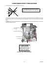
1-1-1 e6nlsp laser beam safety precautions this dvd player uses a pickup that emits a laser beam. The laser beam is emitted from the location shown in the figure. When checking the laser diode, be sure to keep your eyes at least 30 cm away from the pickup lens when the diode is turned on. Do not loo...
Page 169
1-2-1 t1102_isp important safety precautions prior to shipment from the factory, our products are strictly inspected for recognized product safety and electrical codes of the countries in which they are to be sold. However, in order to maintain such compliance, it is equally important to implement t...
Page 170
1-2-2 t1102_isp may be called “horizontal disable” or “hold down.”) read and apply the high voltage limits and, if the chassis is so equipped, the x- radiation protection circuit specifications given on instrument labels and in the product safety & x-radiation warning note on the service data chassi...
Page 171
1-2-3 t1102_isp precautions during servicing a. Parts identified by the # symbol are critical for safety. Replace only with part number specified. B. In addition to safety, other parts and assemblies are specified for conformance with regulations applying to spurious radiation. These must also be re...
Page 172
1-2-4 t1102_isp safety check after servicing examine the area surrounding the repaired location for damage or deterioration. Observe that screws, parts and wires have been returned to original positions. Afterwards, perform the following tests and confirm the specified values in order to verify comp...
Page 173
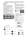
1-3-1 t1102_sn standard notes for servicing circuit board indications 1. The output pin of the 3 pin regulator ics is indicated as shown. 2. For other ics, pin 1 and every fifth pin are indicated as shown. 3. The 1st pin of every male connector is indicated as shown. Instructions for connectors 1. W...
Page 174
1-3-2 t1102_sn • mix of lead-free solder alloy / parts with leaded solder alloy / parts is possible but philips recommends strongly to avoid mixed solder alloy types (leaded and lead-free). If one cannot avoid or does not know whether product is lead-free, clean carefully the solder-joint from old s...
Page 175
1-3-3 t1102_sn with soldering iron: 1. Using desoldering braid, remove the solder from all pins of the flat pack-ic. When you use solder flux which is applied to all pins of the flat pack-ic, you can remove it easily. (fig. S-1-3) 2. Lift each lead of the flat pack-ic upward one by one, using a shar...
Page 176
1-3-4 t1102_sn 2. Installation 1. Using desoldering braid, remove the solder from the foil of each pin of the flat pack-ic on the cba so you can install a replacement flat pack-ic more easily. 2. The “ ●” mark on the flat pack-ic indicates pin 1. (see fig. S-1-7.) be sure this mark matches the 1 on ...
Page 177: Preparation For Servicing
1-4-1 t1102pfs preparation for servicing how to enter the service mode caution 1: 1. Optical sensors system are used for tape start and end sensor on this equipment. Read this page carefully and prepare as described on this page before starting to service; otherwise, the unit may operate unexpectedl...
Page 178
1-5-1 t1102ib operating controls and functions.
Page 179
1-5-2 t1102ib.
Page 180
1-5-3 t1102ib.
Page 181
1-5-4 t1102ib.
Page 182
1-6-1 t0102dc cabinet disassembly instructions 1. Disassembly flowchart this flowchart indicates the disassembly steps for the cabinet parts, and the cba in order to gain access to item(s) to be serviced. When reassembling, follow the steps in reverse order. Bend, route and dress the cables as they ...
Page 183
1-6-2 t0102dc reference notes in the table caution! When removing the crt, be sure to discharge the anode lead of the crt with the crt ground wire before removing the anode cap. 1. Caution 1: discharge the anode lead of the crt with the crt ground wire before removing the anode cap. Disconnect the f...
Page 184
1-6-3 t0102dc wire holder c [5] dvd main cba unit loader cover loader pcb holder [4] dvd mechanism [2] tray chassis unit (s-6) (s-5) (s-5) (s-9) (s-9) top shield (s-10) (s-10) (s-10) [8] deck assembly (s-12) (s-11) (s-13) (s-13) (s-13) [9] main cba (s-8) (s-7) (s-7) (s-7) (s-7) [6] sub cba [7] funct...
Page 185
1-6-4 t0102dc [3] crt anode cap crt cba (s-4) (s-4) (s-4) (s-4) fig. D3 a dvd mechanism fig. D4 view for a short the three short lands by soldering. (either of two places.) connector.
Page 186
1-6-5 t0102dc anode crt gnd dvd main cba unit fe head cylinder assembly ace head assembly capstan motor deck assembly tuner main cba sub cba crt cba to speaker to speaker cl2504a screen cl2501b cn2501 focus cn1802 cl1201 cn1602 cn1301 cn1302 cn1803 cl1402 cn1601 cl1401 cl403 cl2501a cn2571 cn1 cn2 c...
Page 187
1-7-1 t0102ea electrical adjustment instructions general note: “cba” is abbreviation for “circuit board assembly.” note: electrical adjustments are required after replacing circuit components and certain mechanical parts. It is important to perform these adjustments only after all repairs and replac...
Page 188
1-7-2 t0102ea 2. Setting for contrast, color, tint, v-tint and sharp data values general 1. Enter the service mode. (see page 1-7-1.) 2. Press [picture] button on the service remote control unit. Display changes “brt,” “cnt,” “col,” “tnt,” “v-tnt,” and “shp” cyclically when [picture] button is press...
Page 189
1-7-3 t0102ea 4. Setting for y dl time tv, y dl time ext, y sw lpf, black stretch off, black stretch cont and c. Angle data values 1. Enter the service mode. (see page 1-7-1.) 2. Y dl time tv adjustment: press [0] button on the service remote control unit twice to show “d-t tv” on the display. Y dl ...
Page 190
1-7-4 t0102ea 5. Setting for cd-vol, dvd-brt, dvd-cnt and dvd-sharp data values 1. Enter the service mode. (see page 1-7-1.) 2. Cd-vol adjustment: press [vol o] button on the service remote control unit once to show “cd vol” on the display. Dvd-brt adjustment: press [vol o] button on the service rem...
Page 191
1-7-5 t0102ea 6. H f 0 adjustment purpose: to get correct horizontal position and size of screen image. Symptom of misadjustment: horizontal position and size of screen image may not be properly displayed. Note: r2583 --- sub cba 1. Connect frequency counter to r2583. 2. Operate the unit for at leas...
Page 192
1-7-6 t0102ea 8. Setting for 7f data/slp rec/ mono data values 1. Enter the service mode. (see page 1-7-1.) 2. 7f data adjustment: press [vol p] button on the service remote control unit once to show “7f” on the display. Slp rec adjustment: press [vol p] button on the service remote control unit twi...
Page 193
1-7-7 t0102ea 10. Sub-brightness adjustment purpose: to get proper brightness. Symptom of misadjustment: if sub-brightness is incorrect, proper brightness cannot be obtained by adjusting the brightness control. Note: smpte setup level --- 7.5 ire 1. Enter the service mode. (see page 1-7-1.) then inp...
Page 194
1-7-8 t0102ea 13. V. Shift adjustment purpose: to obtain correct vertical position of screen image. Symptom of misadjustment: if v. Position is incorrect, vertical position of image on the screen may not be properly displayed. 1. Enter the service mode. (see page 1-7-1.) press [9] button on the remo...
Page 195
1-7-9 t0102ea the following 2 adjustments normally are not attempted in the field. They should be done only when replacing the crt then adjust as a preparation. 16. Purity adjustment purpose: to obtain pure color. Symptom of misadjustment: if color purity adjustment is incorrect, large areas of colo...
Page 196
1-7-10 t0102ea adjustment points and test points sub cba main cba vr1601 +b adj tp1301 b-out r2583 h adj. Upper focus vr lower screen vr tp2501 (+b adjustment).
Page 197
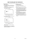
1-8-1 t1102int how to initialize the tv/dvd/vcr to put the program back at the factory-default, initialize the tv/dvd/vcr as the following procedure. 1. Turn the power on and press [select] button on the remote control unit to put the tv/dvd/vcr into dvd mode. 2. Press [1], [2], [3], [4], and [displ...
Page 198: Firmware Renewal Mode
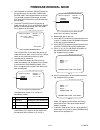
1-9-1 t1102fw firmware renewal mode 1. Turn the power on and press [select] button on the remote control unit to put the tv/dvd/vcr into dvd mode. Then remove the disc on the tray. (it is possible to move to f/w version up mode only when the tv/dvd/vcr is in dvd mode with the tray open.) 2. To put t...
Page 199: Block Diagrams
1-10-1 t0102bls block diagrams system control / servo block diagram contr ol head cl1402 main cba sub cba rf-sw t-reel dv-sync c-sync c-sync v-env ctl(+) d1224 s-led d1204 rec d1216 dvd d1217 tv/vcr p-on+5v rec-led key0 rs1201 remote sensor key1 dvd-led tv/vcr-led reset rota d-rec-h d-rec-h rec-safe...
Page 200
1-10-2 t0102blv video block diagram luminance signal process main cb a video (r)-1 head video (l)-1 head (deck assembly) v(r)-1 v-com1 v(l)-1 cl1401 9 8 7 v(l)-2 v-com2 v(r)-2 6 5 4 q1401 jk1701 video-in tp1401 v-out video agc tuner line rp fbc vxo y/c mix ccd 1h delay r p ynr/comb filter chrominanc...
Page 201
1-10-3 t0102bla audio block diagram rec amp 9 8 au t o bias 11 p-on+5v p-on+5v q1871 bias osc q1872 q1873 (pb=on) q1874 (pb=on) q1875 switching d-rec off 6 5 3 eq amp sp/lp-on p r alc rear tuner fr ont ic1401 (a udio signal pr ocess) 76 4 a-pb/rec cl1402 cn1301 cn2 cn2503 3 a-com 1 ae-h 2 fe-h a udi...
Page 202
1-10-4 t0102blh hi-fi audio block diagram 57 48 47 13 14 69 6 7 r-ch insel l-ch insel nor sw serial data decoder output select vco lpf l-ch bpf r-ch pnr pilot det cont stereo pll stereo filter sap filter sap det sif demod sap demod l-r demod st/sap sw matrix l-ch pnr lim dev comp sw noise vco lpf li...
Page 203
1-10-5 tv process block diagram t0102blt x1301 3.58mhz tp1673 dv d -c cn1302 sa w fil ter sf1001 ic1301 (chr oma/deflection signal pr ocess) tu1001 if ag c sd a scl fsc 1 7 3 2 5 ic1201 (system contr ol/osd) v -sync h-sync osd-r osd-g osd-b 59 58 60 62 63 64 osd-blk sif t o hi-fi a udio block dia g ...
Page 204
1-10-6 crt/h.V. Block diagram t0102blcrt pulse up amp thermal pr o tection 3 6 7 1 5 8 10 7 9 6 green amp blue amp q2503 q2502 q2501 h.Drive q2591 q2571 t2572 v- drive h- drive d. Y . L551 ic2551 (v -deflection contr ol) t2571 f .B .T . Anode focus screen cn2502 cn2503 sub cb a cr t cb a cl2504a r g...
Page 205
1-10-7 power supply block diagram t0102blp line fil ter bridge rectifier t1601 ic1601 err or v o lt a ge det w1601 f1601 4a/125v l1601 d1603 d1606 dega ussing coil cn1601 dg1601 ps1601 ho t cold sub cb a main cb a switching q1601 q1604 q1605 q1683 q1606 q1609 q1607 q1613 q1614 q1688 q1681 q1221 q160...
Page 206: Block Diagrams
1-10-8 block diagrams dvd system control / servo block diagram t0102blsd 12 11 10 d v d-remo te 13 cn1a s d ata cs 60 61 67 d v d-remo te fp-clk fp-din fp-dout 59 d vd main cb a unit drive cb a ic301 (ser v o drive) cn301 m sled motor m spindle motor ic101 (micr o contr oller) + - + - + - + - + - + ...
Page 207
1-10-9 digital signal process block diagram t0102bld 149 c1 6 d1 8 a1 7 b1 5 e1 4 f1 2 d v d-ld 8 cd-ld 10 pd-moni 7 fs(+) 2 fs(-) 3 ts(+) 1 ts(-) 4 cn201 cn201 cn201 ic201 (sw) ic503 (sdram) ic101 (micr o contr oller) fs fs(+) cd/d vd fs(-) ts(+) ts(-) ts pick-up unit detect o r cd/d vd 19 q251,q25...
Page 208
1-10-10 dvd audio block diagram t0102blad ic601 (a udio d/a conver ter) 15 14 cn2a 7 6 8 4 3 2 5 t o d v d system contr o l /ser v o block dia gram t o digit a l signal pr ocess block dia gram au d io serial por t serial contr o l por t 4x/8x o v ersampling digit a l fil ter /function contr o ller e...
Page 209
1-11-1 t1102sc (top view) (bottom view) (bottom view) electrolytic capacitor + transistor or digital transistor npn transistor pnp transistor npn digital transistor pnp digital transistor (top view) (top view) e c b e c b digital transistor e c b (top view) (top view) e c b e c b schematic diagrams ...
Page 210
1-11-2 main 1/6 schematic diagram parts location guide ref no. Position ref no. Position ref no. Position ref no. Position c1203 b-3 d1204 a-2 r1222 a-3 r1270 c-4 c1207 b-1 d1216 a-4 r1223 b-3 r1272 c-4 c1208 a-1 d1217 a-2 r1224 a-4 r1273 c-4 c1210 b-1 d1224 b-4 r1225 a-1 r1274 c-4 c1211 b-1 d1229 e...
Page 211
1-11-3 main 1/6 & sensor schematic diagram t0102scm1 play mode rec mode dvd mode voltage indications for play, rec and dvd modes on the schematic diagrams are as shown below: 1 2 3 5.0 (2.5) 0 > ~ 5.0 the same voltage for play, rec & dvd modes. Indicates that the voltage is not consistent here. “ “ ...
Page 212
1-11-4 t0102scm2 main 2/6 schematic diagram play mode rec mode dvd mode voltage indications for play, rec and dvd modes on the schematic diagrams are as shown below: 1 2 3 5.0 (2.5) 0 > ~ 5.0 the same voltage for play, rec & dvd modes. Indicates that the voltage is not consistent here. “ “ = smd.
Page 213
1-11-5 main 2/6 schematic diagram parts location guide ref no. Position ref no. Position ref no. Position ref no. Position c1410 j-2 c1443 h-3 l1403 g-2 r1419 k-2 c1411 k-2 c1444 h-3 l1404 h-3 r1420 i-1 c1412 k-2 c1445 h-3 l1405 k-4 r1421 i-2 c1413 j-2 c1447 h-4 l1871 g-2 r1422 i-1 c1414 j-2 c1449 k...
Page 214
Main 3/6 schematic diagram parts location guide 1-11-6 ref no. Position ref no. Position ref no. Position ref no. Position c1001 q-1 c1322 n-2 l1032 p-1 r1317 n-4 c1002 q-1 c1323 n-2 l1033 q-2 r1320 n-2 c1003 q-1 c1325 n-2 l1302 q-3 r1329 m-4 c1004 p-1 c1332 n-2 r1333 n-2 c1005 q-1 c1333 n-2 q1350 q...
Page 215
1-11-7 t0102scm3 main 3/6 schematic diagram play mode rec mode dvd mode voltage indications for play, rec and dvd modes on the schematic diagrams are as shown below: 1 2 3 5.0 (2.5) 0 > ~ 5.0 the same voltage for play, rec & dvd modes. Indicates that the voltage is not consistent here. “ “ = smd.
Page 216
1-11-8 t0102scm4 main 4/6 schematic diagram play mode rec mode dvd mode voltage indications for play, rec and dvd modes on the schematic diagrams are as shown below: 1 2 3 5.0 (2.5) 0 > ~ 5.0 the same voltage for play, rec & dvd modes. Indicates that the voltage is not consistent here. “ “ = smd.
Page 217
Main 4/6 schematic diagram parts location guide 1-11-9 ref no. Position ref no. Position ref no. Position ref no. Position c1701 v-4 c1768 v-3 c1793 t-2 r1756 v-2 c1722 v-1 c1769 v-4 c1794 v-2 r1757 s-3 c1732 v-1 c1770 v-4 c1795 t-2 r1758 t-3 c1740 u-1 c1771 v-4 c1796 t-1 r1759 t-2 c1747 v-3 c1772 u...
Page 218
Main 5/6 schematic diagram parts location guide 1-11-10 ref no. Position ref no. Position ref no. Position c1112 aa-2 cn1802 x-4 r1801 y-4 c1113 z-2 cn1803 bb-4 r1802 y-4 c1114 aa-1 r1803 aa-2 c1115 aa-2 d1811 y-1 r1808 aa-2 c1116 aa-2 d1812 z-1 r1809 y-1 c1117 z-2 d1813 z-1 r1810 y-1 c1118 z-2 r181...
Page 219
1-11-11 t0102scm5 main 5/6 schematic diagram play mode rec mode dvd mode voltage indications for play, rec and dvd modes on the schematic diagrams are as shown below: 1 2 3 5.0 (2.5) 0 > ~ 5.0 the same voltage for play, rec & dvd modes. Indicates that the voltage is not consistent here. “ “ = smd.
Page 220
1-11-12 t0102scm6 main 6/6 schematic diagram play mode rec mode dvd mode voltage indications for play, rec and dvd modes on the schematic diagrams are as shown below: 1 2 3 5.0 (2.5) 0 > ~ 5.0 the same voltage for play, rec & dvd modes. Indicates that the voltage is not consistent here. “ “ = smd no...
Page 221
1-11-13 main 6/6 schematic diagram parts location guide ref no. Position ref no. Position ref no. Position ref no. Position c1604 dd-3 d1611 dd-2 q1604 ee-1 r1638 ee-2 c1605 cc-3 d1613 ee-4 q1605 ff-1 r1639 ff-2 c1606 dd-3 d1614 ee-3 q1606 ff-1 r1640 ff-1 c1607 dd-3 d1615 ee-2 q1607 ff-1 r1641 ff-1 ...
Page 222
Main cba parts location guide 1-11-14 ref no. Position ref no. Position ref no. Position ref no. Position ref no. Position ref no. Position c1001 f-1 c1257 a-4 c1450 b-4 c1766 c-4 d1224 c-3 ic1201 b-3 c1002 g-1 c1258 b-5 c1452 c-4 c1767 d-4 d1229 c-1 ic1202 b-4 c1003 g-1 c1261 a-4 c1461 d-3 c1768 d-...
Page 223
Dvd-y tp1672 wf17 dvd-c tp1673 wf18 v-out tp1401 wf5 pin 59 of ic1201 wf16 wf15 pin 58 of ic1201 tp1301 b-out +b adj vr1601 to sensor cba (start-sensor) to sensor cba (end-sensor) main cba top view because a hot chassis ground is present in the power supply circuit, an isolation transformer must be ...
Page 224
Wf7 pin 49 of ic1401 pin 32 of ic1401 pin 9 of ic1401 wf8 wf4 wf2 pin 10 of ic1401 rf-sw tp1402 wf1 ctl-amp-out tp1202 wf3 dvd-audio-l tp1001 wf19 env. Jm1403 wf6 1-11-16 main cba bottom view because a hot chassis ground is present in the power supply circuit, an isolation transformer must be used. ...
Page 225
T0102sccrt t0102scf function schematic diagram function schematic diagram parts location guide ref no. Position ref no. Position cn2401 a-1 sw2401 a-2 cn2801 c-1 sw2402 b-2 sw2403 b-2 r2401 a-2 sw2404 b-2 r2402 b-2 sw2405 b-2 r2403 b-2 sw2406 c-2 r2404 b-2 sw2407 c-2 r2405 b-2 sw2408 c-2 r2406 c-2 r...
Page 226
Wf13 q2502 collector wf12 q2503 collector wf14 q2501 collector 1-11-18 crt cba top view crt cba bottom view bt1100f01022-b crt cba parts location guide ref no. Position ref no. Position ref no. Position ref no. Position c2504 a-2 d2501 a-2 r2502 a-1 r2515 a-1 c2505 a-1 d2502 a-2 r2503 a-1 r2516 a-1 ...
Page 227
Function cba top view function cba bottom view bt1100f01022-c junction cba bottom view junction cba top view bt1100f01022 1-11-19 ref no. Position cn2401 d-1 cn2801 a-1 r2401 d-1 r2402 c-1 r2403 c-1 r2404 b-1 r2405 b-1 r2406 b-1 r2407 b-1 sw2401 d-1 sw2402 c-1 sw2403 c-1 sw2404 c-1 sw2405 b-1 sw2406...
Page 228
1-11-20 t0102scsub1 sub 1/2 schematic diagram play mode rec mode dvd mode voltage indications for play, rec and dvd modes on the schematic diagrams are as shown below: 1 2 3 5.0 (2.5) 0 > ~ 5.0 the same voltage for play, rec & dvd modes. Indicates that the voltage is not consistent here..
Page 229
Sub 1/2 schematic diagram parts location guide 1-11-21 ref no. Position ref no. Position ref no. Position ref no. Position c2531 c-4 d2571 b-3 r2551 a-3 r2586 e-2 c2533 d-4 d2572 d-2 r2552 b-3 r2587 d-2 c2552 b-3 d2584 e-1 r2555 e-1 r2588 e-2 c2553 b-2 d2585 e-2 r2556 b-3 r2589 b-1 c2555 a-3 d2586 e...
Page 230
1-11-22 sub 2/2 schematic diagram parts location guide ref no. Position ref no. Position ref no. Position ref no. Position c2601 k-3 d2603 h-2 q2615 h-2 r2671 i-2 c2604 h-1 d2613 k-2 q2616 h-1 r2672 i-2 c2610 k-3 d2625 h-1 q2617 i-2 r2673 j-2 c2616 k-2 d2627 k-1 r2675 g-1 c2618 k-3 d2648 i-2 r2613 k...
Page 231
1-11-23 sub 2/2 schematic diagram t0102scsub2 play mode rec mode dvd mode voltage indications for play, rec and dvd modes on the schematic diagrams are as shown below: 1 2 3 5.0 (2.5) 0 > ~ 5.0 the same voltage for play, rec & dvd modes. Indicates that the voltage is not consistent here..
Page 232
Sub cba parts location guide ref no. Position ref no. Position ref no. Position ref no. Position ref no. Position ref no. Position ref no. Position c2531 c-1 c2618 c-4 d2597 a-2 q2592 a-2 r2563 b-3 r2598 a-2 r2684 a-4 c2533 c-1 c2625 c-4 d2598 a-2 q2610 b-4 r2564 b-3 r2599 a-2 r2685 a-4 c2552 c-2 c2...
Page 233
R2583 (h f 0 adjustment) +b tp2501 j2550 gnd sub cba top view bt1100f01022-a 1-11-25.
Page 234
H-drive tp2503 wf11 pin 5 cn2571 q2571 collector wf10 wf9 wf20 j2537 spdif 1-11-26 bt1100f01022-a sub cba bottom view.
Page 235
1-11-27 t0102scd1 dvd main 1/3 schematic diagram 3 5.0 (2.5) play mode stop mode voltage indications for play and stop modes on the schematic diagrams are as shown below: 1 2 ~ 5.0 the same voltage for both play & stop modes. Indicates that the voltage is not consistent here. “ “ = smd 1 note: eithe...
Page 236
1-11-28 t0102scd2 dvd main 2/3 schematic diagram 3 5.0 (2.5) play mode stop mode voltage indications for play and stop modes on the schematic diagrams are as shown below: 1 2 ~ 5.0 the same voltage for both play & stop modes. Indicates that the voltage is not consistent here. “ “ = smd.
Page 237
1-11-29 ic101 voltage chart pin.No play stop pin.No play stop pin.No play stop pin.No play stop 1 ~ ~ 33 ~ ~ 65 ----- ----- 97 ----- ----- 2 ~ ~ 34 3.4 3.4 66 3.4 3.5 98 3.4 3.4 3 0 0 35 0 0 67 3.2 3.2 99 0.9 0.8 4 ~ ~ 36 ~ ~ 68 ----- ----- 100 0 0 5 ~ ~ 37 ~ ~ 69 3.4 3.4 101 2.4 2.4 6 3.4 3.4 38 0....
Page 238
1-11-30 t0102scd3 dvd main 3/3 schematic diagram 3 5.0 (2.5) play mode stop mode voltage indications for play and stop modes on the schematic diagrams are as shown below: 1 2 ~ 5.0 the same voltage for both play & stop modes. Indicates that the voltage is not consistent here. “ “ = smd.
Page 239: Waveforms
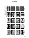
X6twf waveforms 1-12-1 wf2 wf1 wf5 wf4 wf8 wf7 wf3 wf9 wf11 wf13 wf14 wf10 wf15 wf16 wf12 wf18 wf17 wf19 wf20 spdifspdif 1v 0.1 µ secsec input: ntsc color bar signal (with 1khz audio signal) --- wf1~wf16 dvd video (power on (stop) mode) --- wf17, wf18 cd (1khz play) --- wf19, wf20 initial position: ...
Page 240: Wiring Diagram
T0102wit 1-13-1 wiring diagram 1 2 5 5 cr t cb a focus screen gnd l551 d. Y . Hd vd cl2501a cl2501b main cb a sub cb a cn1302 cn2501 w1601 cn1601 1 2 3 4 5 t2571 fbt cl2504a anode 1 3 4 1 2 3 4 cl2504b cn2504 cn2571 junction cb a sp1801 speaker r-ch cl1802 full erase head cl403 fe head a u dio head ...
Page 241: Wiring Diagram
Wiring diagram 1-13-2 t0102wid dvd main cba unit continue wiring diagram to cn1 cn301 3 4 tra y -in gnd sl(-) 5 6 sp(-) 7 sp(+) 8 sl(+) tray-in drive cba m sled motor m spindle motor ev+1.2v ev+1.2v ev+3.3v dvd-on+3.3v dvd-on+5v ev+9v gnd 1 2 3 4 5 6 7 gnd gnd pwrcon 8 15 9 10 11 12 cn1a pick up uni...
Page 242
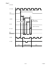
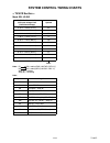
1-14-1 t1102ti system control timing charts mode sw: ld-sw note: ej rs: loading fwd (lm-fwd / rev “h”) rs ej: loading rev (lm-fwd / rev “l”) stop (a) = loading stop (b) = unloading note: ld-sw position detection a/d input voltage limit (calculated voltage) symbol 3.76 v ~ 4.50 v (4.12 v) ej 4.51 v ~...
Page 243
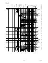
1-14-2 t1102ti chart 1 18 rf-sw f-ad ( internal signal ) c-drive pb ctl 66 c-f/r still still frame advance roll compensation (drum servo) h-a-sw 15 rota at the first rise of rf-sw after a rise in f-ad signal. St t1 bl "h" "h" t2 "z" 1) sp mode 1 2 3 4 acceleration detection stop detection slow track...
Page 244
1-14-3 t1102ti chart 2 18 rf-sw f-ad ( internal signal ) c-drive pb ctl 66 c-f/r still still frame advance roll compensation (drum servo) h-a-sw 15 rota at the first rise of rf-sw after a rise in f-ad signal. St t1 bl "h" "h" t2 "z" 2) lp/ep mode 1 2 3 4 acceleration detection stop detection slow tr...
Page 245
1-14-4 t1102ti chart 3 +100ms(ntsc) +620ms(p al) 1. Eject (po wer off) -> cassette in (po wer on) -> st op(b) -> st op(a) -> pla y -> rs -> fs -> pla y -> still/slo w -> pla y -> st op( a) eject cass.Load st-s/ end-s "off" play rew ff play play stop /eject 0.2s 0.4s 0.2s ld-fwd stop(a) stop(a) ld-fw...
Page 246
1-14-5 t1102ti chart 4 pin no . Ld-sw cl/ss ld-cont c-drive "z" on on c-f/r dr um r o t a tion p-on-h a-mute d-rec-h d-pb-h ej au rs sf sm tl fb al sb 1 82 66 31 65 44 displa y st-s "on" rec rew ff stop /eject 0.5s 1.0s 0.2s 0.2s 0.5s 0.2s 0.5s 0.5s 0.5s 0.2s 0.2s 0.2s 1.5s 2.5s short rev 1.0s 0.2s ...
Page 247
1-14-6 t1102ti tray in (tl221) sled drive (tp303) disc drive (tp301) focus drive (tp304) tracking drive (tp302) 0v 3.3v 0v 1.65v 0v 0v 0v 1.65v 1.65v 1.65v tray close ~ play / play ~ tray open tray close disc rotation play disc stop tray open.
Page 248
1-15-1 t0102pin ic pin function descriptions ic1201 (tv/vcr micro controller ic) “h” ≥ 4.5 v, “l” ≤ 1.0 v pin no. In/ out signal name function 1 in ld-sw loading switch input 2 out dvd-led dvd-led output 3 in p-safety 2 power supply failure detection 2 4 in st/sap-in tuner stereo/sap detector signal...
Page 249
1-15-2 t0102pin 71 out scl e2prom/chroma ic tuner communication clock 72 in/ out sda e2prom/chroma ic tuner communication data 73 - nu not used 74 in c-sync c-sync input 75 - nu not used 76 out c-cont capstan motor control signal 77 out d-cont drum motor control signal 78 in p-safety 3 power supply ...
Page 250: Lead Identifications
1-16-1 t0102le lead identifications e c b e c b e c b 80 51 81 100 1 30 50 31 5 4 8 1 e c 60 21 40 41 20 1 80 61 1 2 3 4 1: vin 2: vo 3: gnd 4: vc 8 5 1 4 1 7 la78040a an15524a 1 2 4 3 1: a 2: k 3: e 4: c 1 2 3 1: r 2: a 3: k 1: in 2: gnd 3: out 1 2 3 2sa1175(f) 2sa950(o,y) 2sc1627y-tpe2 2sc2785(f) ...
Page 251
1-17-1 electrical parts list miscellaneous 9965 000 28878 dvd main cba unit 9965 000 29338 mps cba 9965 000 28880 mma cba 9965 000 28882 sensor cba mps cba unit mps cba unit consists of sub cba, crt cba, function cba and junction cba sub cba miscellaneous bc2501 9965 000 13874 bead inductors fba04ha...
Page 252
Electrical parts list 1-17-2 transistors q2610 * 4822 130 11101 2sa1015gr q2611 9965 000 10994 2sc3199-gr/ktc3199-gr q2611 * 4822 130 41306 2sc1815gr q2612 9965 000 05643 transistor 2sc2785(f) q2612 * 9965 000 10994 2sc3199-gr/ktc3199-gr q2612 * 4822 130 41306 2sc1815gr q2615 9965 000 29024 transist...
Page 253
Electrical parts list 1-17-3 mma cba unit mma cba unit consists of main cba and sensor cba main cba miscellaneous bc1600 9965 000 13875 bead inductors fbr07ha121tb-00 bc1605 9965 000 13874 bead inductors fba04ha600vb-00 bc1606 9965 000 13875 bead inductors fbr07ha121tb-00 bc1607 9965 000 13874 bead ...
Page 254
Capacitors 1-17-4 c1619 * 9965 000 28898 elcap. 1000uf/16v m(vr/hc) c1620 9965 000 25495 electrolytic cap. 1000uf/16v m c1620 * 9965 000 28898 elcap. 1000uf/16v m(vr/hc) c1630! 9965 000 28899 ! Safety cap. 4700pf/250v kx c1643 9965 000 24154 electrolytic cap. 1000uf/6.3v m c1643 * 9965 000 25351 ele...
Page 255
D1350 * 4822 130 30621 1n4148 d1351 4822 130 32778 1ss133 d1351 * 4822 130 30621 1n4148 d1353 9965 000 24180 zener diode mtzjt-779.1b d1353 * 9965 000 28908 zener diode dz-9.1bsbt265 d1419 4822 130 32778 1ss133 d1419 * 4822 130 30621 1n4148 d1420 4822 130 32778 1ss133 d1420 * 4822 130 30621 1n4148 d...
Page 256
Q1402 * 4822 130 11101 2sa1015gr q1403 9965 000 05644 transistor 2sa1175(f) q1403 * 4822 130 10462 kta1267-gr q1403 * 4822 130 11101 2sa1015gr q1404 9965 000 05643 transistor 2sc2785(f) q1404 * 9965 000 10994 2sc3199-gr/ktc3199-gr q1404 * 4822 130 41306 2sc1815gr q1601! 9965 000 25510 ! Mos fet 2sk3...
Page 257
1-18-1 t0102cex exploded views cabinet l1 l1 l1 a2 a3 l1 l1 l3-2 l1 l3-1 b5 b5 l2 l4 l4 a1-7 a1-9 a1-8 a1-5 a1-6 a1-4 a1-3 a1-1 a1x a1-2 b7 b6 cl1802 l4 l4 sp801 cl2801 b6 sp1801 tb1 tb17 tb10 tl14 tl1-4 tl1-4 tl1-3 tl1-1 tl1-1 tl3 tl4 tl5 tb14 tl3 tl1-1 tl1-2 tl1-2 dl2 db5 db2 tb3 tb7 tb13 tb30 tl1...
Page 258
1-18-2 t0102pex fr ont s4 s4 s1 x1 tape x9 s4 x4 x2-1 x25 x3 s3 s6 s7 s2 packing tape x2-2 packing.
Page 259
1-19-1 mechanical set & accessory parts list electrical parts 9965 000 28878 dvd main cba unit 9965 000 29338 mps cba 9965 000 28880 mma cba 9965 000 28882 sensor cba dg601! 9965 000 29335 ! Degaussing coil avdg172 dg601! * 9965 000 29336 ! Degaussing coil f-55 dg601! * 9965 000 29337 ! Degaussing c...
Page 260: Deck Mechanism Section
Deck mechanism section color tv with built-in vcr/dvd player table of contents standard maintenance. . . . . . . . . . . . . . . . . . . . . . . . . . . . . . . . . . . . . . . . . . . . . . . . . . . . . . . . . . . . . . 2-1-1 service fixture and tools . . . . . . . . . . . . . . . . . . . . . . ....
Page 261: Standard Maintenance
2-1-1 n2466ftmen standard maintenance service schedule of components this maintenance chart shows you the standard of replacement and cleaning time for each part. Because those may replace depending on environment and purpose for use, use the chart for reference. Notes: 1. Clean all parts for the ta...
Page 262
2-1-2 n2466ftmen cleaning cleaning of video head clean the head with a head cleaning stick or chamois cloth. Procedure 1. Remove the top cabinet. 2. Put on a glove (thin type) to avoid touching the upper and lower drum with your bare hand. 3. Put a few drops of 90% ethyl alcohol on the head cleaning...
Page 263: Service Fixture And Tools
2-2-1 mk14fix_pc service fixture and tools vfms0001h6 alignment tape back tension meter (made in usa) flat screw driver (purchase locally) post adjustment screwdriver metric thickness gauges (purchase locally) lock screw driver (purchase locally) head cleaning stick.
Page 264
2-3-1 mk14nma_pc mechanical alignment procedures explanation of alignment for the tape to correctly run starts on the next page. Refer to the information below on this page if a tape gets stuck, for example, in the mechanism due to some electrical trouble of the unit. Service information a. Method f...
Page 265
2-3-2 mk14nma_pc 1. Tape interchangeability alignment note: to do these alignment procedures, make sure that the tracking control circuit is set to the preset position every time a tape is loaded or unloaded. (refer to page 2-3-4, procedure 1-c, step 2.) equipment required: dual trace oscilloscope v...
Page 266
2-3-3 mk14nma_pc 1-a. Preliminary/final checking and alignment of tape path purpose: to make sure that the tape path is well stabilized. Symptom of misalignment: if the tape path is unstable, the tape will be damaged. Note: do not use an alignment tape for this procedure. If the unit is not correctl...
Page 267
2-3-4 mk14nma_pc 5. To shift the ctl waveform, press [channel k] or [channel l] buttons on the unit. Then make sure that the maximum output position of pb fm envelope signal become within ± 2ms from preset position. 6. Set the tracking control circuit to the preset position by pressing [channel k] b...
Page 268
2-3-5 mk14nma_pc 1-d. Azimuth alignment of audio/control/ erase head purpose: to correct the azimuth alignment so that the audio/control/erase head meets tape tracks properly. Symptom of misalignment: if the position of the audio/control/erase head is not properly aligned, the audio s/n ratio or fre...
Page 269: Of Deck Mechanism
2-4-1 n2466ftda disassembly/assembly procedures of deck mechanism before following the procedures described below, be sure to remove the deck assembly from the cabinet. (refer to cabinet disassembly instructions of main section.) all the following procedures, including those for adjustment and repla...
Page 270
2-4-2 n2466ftda (1): follow steps in sequence. When reassembling, follow the steps in reverse order. These numbers are also used as identification (location) no. Of parts in the figures. (2): indicates the part to start disassembling with in order to disassemble the part in column (1). (3): name of ...
Page 271
2-4-3 n2466ftda [14] [13] [11] [10] [12] [7] [8] [30] [40] [16] [39] [38] [42] [41] [43] [9] [34] [15] [36] [35] [29] [46] fig. Dm1 top view [32] [20] [33] [24] [25] [27] [26] [23] [28] [31] [21] [22] bottom view fig. Dm2.
Page 272
2-4-4 n2466ftda [1] (s-1) (s-1) fig. Dm3 locking tab view for a first, while pushing the locking tab as shown at right, slide and pull up the right side on [2] to release pin a and pin b from the slots a. Then, remove pin c and pin d on [2] from the slots b as shown. Slot a slots b pin a slot a pin ...
Page 273
2-4-5 n2466ftda desolder from bottom lead with red stripe view for a (s-2) [7] (l-14) [46] [47] a fig. Dm6 view for a desolder from bottom lead with white stripe a [8] [9] (s-4) (s-3) ldg belt [8] fig. Dm7 pin of [12] pin of [10] groove of [28] view for a when reassembling [10] and [12], confirm tha...
Page 274
2-4-6 n2466ftda installation of [13] and [12] pin of [12] groove of [28] hook spring (p-3) up to [12] and [13], then install then to the specified position so that [12] will be floated slightly while holding [12] and [13]. (refer to fig. A.) fig. A [13] [12] (p-3) fig. B (top view) install pin of [1...
Page 275
2-4-7 n2466ftda [20] (s-8) cap belt [20] [21] cap belt a installation position of cap belt view for a fig. Dm11 (l-6) [22] [23] (p-5) [21] (c-1) (c-2) (p-5) [28] when installing [23], install the spring (p-5) to [28] as shown in the left figure, and then install [23] while pressing the spring (p-5) ...
Page 276
2-4-8 n2466ftda [24] (c-4) (s-9) [25] [27] [26] [28] (c-3) (l-8) (l-9) (l-10) fig. Dm13-1 pin of [34] pin of [31] position of mode lever when installed pin of [35] align [25] and [28] as shown. Bottom view [28] [25] [28] top view first tooth on [44] first groove on [28] installation of [25] when rea...
Page 277
2-4-9 n2466ftda [43] [41] [42] (l-13) fig. Dm16 [44] [45] slide (p-9) fig. Dm17.
Page 278
2-5-1 mk14napm_pc alignment procedures of mechanism the following procedures describe how to align the individual gears and levers that make up the tape loading/unloading mechanism. Since information about the state of the mechanism is provided to the system control circuit only through the mode swi...
Page 279: Deck Exploded Views
2-6-1 n2466ftdex deck exploded views deck mechanism view 1 mark description floil g-684g or multemp mh-d (blue grease) slidus oil #150 b12 b492 b11 b571 b37 some ref. Numbers are not in sequence. B126 b8 b121 b426 b560 l1450 l1450 l1466 b501 chassis assembly top view (lubricating point) chassis asse...
Page 280
2-6-2 n2466ftdex deck mechanism view 2 mark description floil g-684g or multemp mh-d (blue grease) slidus oil #150 sankoul fg84m (yellow grease) b508 b414 view for a (grease point) b516 b559 b52 b134 b133 b568 b565 b417 some ref. Numbers are not in sequence. Bottom side (grease point) b507 b488 b570...
Page 281
2-6-3 n2466ftdex deck mechanism view 3 mark description floil g-684g or multemp mh-d (blue grease) slidus oil #150 b563 b300 b562 b482 b355 b354 b483 b425 l1321 b347 l1321 b313 l1341 b303 b555 b514 some ref. Numbers are not in sequence. B361 b359 b529 b360 b561 l1474.
Page 282
2-7-1 mechanical parts list - vcr mechanism b2 9965 000 29043 cylinder assy mk12.5 ntsc 6hd b2 * 9965 000 29044 cylinder assy mk12.5 ntsc 6hd b3 9965 000 23363 loading motor assembly mk12.5 b8 9965 000 17191 pulley assembly mk12 b9 9965 000 23364 moving guide s p.P mk12.5 b10 9965 000 23365 moving g...
Page 283: 19Mdtr20/
Contents chapter survey of versions: published by fu-kc 0522 service av systems printed in the netherlands subject to modification /17 ntsc color tv with built-in vcr/dvd player 19mdtr20/ 17 c copyright 2005 philips consumer electronics b.V. Eindhoven, the netherlands. All rights reserved. No part o...
Page 284: Main Section
Main section color tv with built-in vcr/dvd player table of contents laser beam safety precautions . . . . . . . . . . . . . . . . . . . . . . . . . . . . . . . . . . . . . . . . . . . . . . . . . . . . 1-1-1 important safety precautions. . . . . . . . . . . . . . . . . . . . . . . . . . . . . . . ....
Page 285
1-1-1 e6nlsp laser beam safety precautions this dvd player uses a pickup that emits a laser beam. The laser beam is emitted from the location shown in the figure. When checking the laser diode, be sure to keep your eyes at least 30 cm away from the pickup lens when the diode is turned on. Do not loo...
Page 286
1-2-1 t1102_isp important safety precautions prior to shipment from the factory, our products are strictly inspected for recognized product safety and electrical codes of the countries in which they are to be sold. However, in order to maintain such compliance, it is equally important to implement t...
Page 287
1-2-2 t1102_isp may be called “horizontal disable” or “hold down.”) read and apply the high voltage limits and, if the chassis is so equipped, the x- radiation protection circuit specifications given on instrument labels and in the product safety & x-radiation warning note on the service data chassi...
Page 288
1-2-3 t1102_isp precautions during servicing a. Parts identified by the # symbol are critical for safety. Replace only with part number specified. B. In addition to safety, other parts and assemblies are specified for conformance with regulations applying to spurious radiation. These must also be re...
Page 289
1-2-4 t1102_isp safety check after servicing examine the area surrounding the repaired location for damage or deterioration. Observe that screws, parts and wires have been returned to original positions. Afterwards, perform the following tests and confirm the specified values in order to verify comp...
Page 290
1-3-1 t1102_sn standard notes for servicing circuit board indications 1. The output pin of the 3 pin regulator ics is indicated as shown. 2. For other ics, pin 1 and every fifth pin are indicated as shown. 3. The 1st pin of every male connector is indicated as shown. Instructions for connectors 1. W...
Page 291
1-3-2 t1102_sn • mix of lead-free solder alloy / parts with leaded solder alloy / parts is possible but philips recommends strongly to avoid mixed solder alloy types (leaded and lead-free). If one cannot avoid or does not know whether product is lead-free, clean carefully the solder-joint from old s...
Page 292
1-3-3 t1102_sn with soldering iron: 1. Using desoldering braid, remove the solder from all pins of the flat pack-ic. When you use solder flux which is applied to all pins of the flat pack-ic, you can remove it easily. (fig. S-1-3) 2. Lift each lead of the flat pack-ic upward one by one, using a shar...
Page 293
1-3-4 t1102_sn 2. Installation 1. Using desoldering braid, remove the solder from the foil of each pin of the flat pack-ic on the cba so you can install a replacement flat pack-ic more easily. 2. The “ ●” mark on the flat pack-ic indicates pin 1. (see fig. S-1-7.) be sure this mark matches the 1 on ...
Page 294: Preparation For Servicing
1-4-1 t1102pfs preparation for servicing how to enter the service mode caution 1: 1. Optical sensors system are used for tape start and end sensor on this equipment. Read this page carefully and prepare as described on this page before starting to service; otherwise, the unit may operate unexpectedl...
Page 295
1-5-1 t1102ib operating controls and functions note: front cabinet and rear cabinet illustrations differ from the actual model since these pages are made extracts from the owners manual..
Page 296
1-5-2 t1102ib.
Page 297
1-5-3 t1102ib.
Page 298
1-5-4 t1102ib.
Page 299
1-6-1 t0102dc cabinet disassembly instructions 1. Disassembly flowchart this flowchart indicates the disassembly steps for the cabinet parts, and the cba in order to gain access to item(s) to be serviced. When reassembling, follow the steps in reverse order. Bend, route and dress the cables as they ...
Page 300
1-6-2 t0102dc reference notes in the table caution! When removing the crt, be sure to discharge the anode lead of the crt with the crt ground wire before removing the anode cap. 1. Caution 1: discharge the anode lead of the crt with the crt ground wire before removing the anode cap. Disconnect the f...
Page 301
1-6-3 t0102dc wire holder c [5] dvd main cba unit loader cover loader pcb holder [4] dvd mechanism [2] tray chassis unit (s-6) (s-5) (s-5) (s-9) (s-9) top shield (s-10) (s-10) (s-10) [8] deck assembly (s-12) (s-11) (s-13) (s-13) (s-13) [9] main cba (s-8) (s-7) (s-7) (s-7) (s-7) [6] sub cba [7] funct...
Page 302
1-6-4 t0102dc [3] crt anode cap crt cba (s-4) (s-4) (s-4) (s-4) fig. D3 a dvd mechanism fig. D4 view for a short the three short lands by soldering. (either of two places.) connector.
Page 303
1-6-5 t0102dc anode crt gnd dvd main cba unit fe head cylinder assembly ace head assembly capstan motor deck assembly tuner main cba sub cba crt cba to speaker to speaker cl2504a screen cl2501b cn2501 focus cn1802 cl1201 cn1602 cn1301 cn1302 cn1803 cl1402 cn1601 cl1401 cl403 cl2501a cn2571 cn1 cn2 c...
Page 304
1-7-1 t0102mcea electrical adjustment instructions general note: “cba” is abbreviation for “circuit board assembly.” note: electrical adjustments are required after replacing circuit components and certain mechanical parts. It is important to perform these adjustments only after all repairs and repl...
Page 305
1-7-2 t0102mcea 2. Setting for contrast, color, tint, v-tint and sharp data values general 1. Enter the service mode. (see page 1-7-1.) 2. Press [picture] button on the service remote control unit. Display changes “brt,” “cnt,” “col,” “tnt,” “v-tnt,” and “shp” cyclically when [picture] button is pre...
Page 306
1-7-3 t0102mcea 4. Setting for y dl time tv, y dl time ext, y sw lpf, black stretch off, black stretch cont and c. Angle data values 1. Enter the service mode. (see page 1-7-1.) 2. Y dl time tv adjustment: press [0] button on the service remote control unit twice to show “d-t tv” on the display. Y d...
Page 307
1-7-4 t0102mcea 5. Setting for cd-vol, dvd-brt, dvd-cnt and dvd-sharp data values 1. Enter the service mode. (see page 1-7-1.) 2. Cd-vol adjustment: press [vol o] button on the service remote control unit once to show “cd vol” on the display. Dvd-brt adjustment: press [vol o] button on the service r...
Page 308
1-7-5 t0102mcea 6. H f 0 adjustment purpose: to get correct horizontal position and size of screen image. Symptom of misadjustment: horizontal position and size of screen image may not be properly displayed. Note: r2583 --- sub cba 1. Connect frequency counter to r2583. 2. Operate the unit for at le...
Page 309
1-7-6 t0102mcea 8. Setting for 7f data/slp rec/ mono data values 1. Enter the service mode. (see page 1-7-1.) 2. 7f data adjustment: press [vol p] button on the service remote control unit once to show “7f” on the display. Slp rec adjustment: press [vol p] button on the service remote control unit t...
Page 310
1-7-7 t0102mcea 10. Sub-brightness adjustment purpose: to get proper brightness. Symptom of misadjustment: if sub-brightness is incorrect, proper brightness cannot be obtained by adjusting the brightness control. Note: smpte setup level --- 7.5 ire 1. Enter the service mode. (see page 1-7-1.) then i...
Page 311
1-7-8 t0102mcea 13. V. Shift adjustment purpose: to obtain correct vertical position of screen image. Symptom of misadjustment: if v. Position is incorrect, vertical position of image on the screen may not be properly displayed. 1. Enter the service mode. (see page 1-7-1.) press [9] button on the re...
Page 312
1-7-9 t0102mcea the following 2 adjustments normally are not attempted in the field. They should be done only when replacing the crt then adjust as a preparation. 16. Purity adjustment purpose: to obtain pure color. Symptom of misadjustment: if color purity adjustment is incorrect, large areas of co...
Page 313
1-7-10 t0102mcea adjustment points and test points sub cba main cba vr1601 +b adj tp1301 b-out r2583 h adj. Upper focus vr lower screen vr tp2501 (+b adjustment).
Page 314
1-8-1 t1102int how to initialize the tv/dvd/vcr to put the program back at the factory-default, initialize the tv/dvd/vcr as the following procedure. 1. Turn the power on and press [select] button on the remote control unit to put the tv/dvd/vcr into dvd mode. 2. Press [1], [2], [3], [4], and [displ...
Page 315: Firmware Renewal Mode
1-9-1 t1102fw firmware renewal mode 1. Turn the power on and press [select] button on the remote control unit to put the tv/dvd/vcr into dvd mode. Then remove the disc on the tray. (it is possible to move to f/w version up mode only when the tv/dvd/vcr is in dvd mode with the tray open.) 2. To put t...
Page 316: Block Diagrams
1-10-1 t0102mcbls block diagrams system control / servo block diagram contr ol head cl1402 ace head assembly main cba sub cba rf-sw t-reel dv-sync c-sync c-sync v-env ctl(+) d1224 s-led d1204 rec d1216 dvd d1217 tv/vcr p-on+5v rec-led key0 rs1201 remote sensor key1 dvd-led tv/vcr-led reset rota d-re...
Page 317
1-10-2 t0102mcblv video block diagram luminance signal process main cb a video (r)-1 head video (l)-1 head (deck assembly) v(r)-1 v-com1 v(l)-1 cl1401 9 8 7 v(l)-2 v-com2 v(r)-2 6 5 4 q1401 jk1701 video-in tp1401 v-out video agc tuner line rp fbc vxo y/c mix ccd 1h delay r p ynr/comb filter chromina...
Page 318
1-10-3 t0102mcbla audio block diagram rec amp 9 8 au t o bias 11 p-on+5v p-on+5v q1871 bias osc q1872 q1873 (pb=on) q1874 (pb=on) q1875 switching d-rec off 6 5 3 eq amp sp/lp-on p r alc rear tuner fr ont ic1401 (a udio signal pr ocess) 76 4 a-pb/rec cl1402 cn1301 cn2 cn2503 3 a-com 1 ae-h 2 fe-h a u...
Page 319
1-10-4 t0102mcblh hi-fi audio block diagram n-a-out audio-out(r) audio-out(l) n-a-in hi-fi-h-sw hi-fi mute normal-h st/sap-in to audio block diagram scl hi-fi audio (r) head hi-fi audio (l) head cylinder assembly main cba cl1401 ic1701 (mts/ sap/ hi-fi audio process/ hi-fi head amp) to audio block d...
Page 320
1-10-5 tv process block diagram t0102mcblt x1301 3.58mhz tp1673 dv d -c cn1302 sa w fil ter sf1001 ic1301 (chr oma/deflection signal pr ocess) tu1001 if ag c sd a scl fsc 1 7 3 2 5 ic1201 (system contr ol/osd) v -sync h-sync osd-r osd-g osd-b 59 58 60 62 63 64 osd-blk sif t o hi-fi a udio block dia ...
Page 321
1-10-6 crt/h.V. Block diagram t0102mcblcrt pulse up amp thermal pr o tection 3 6 7 1 5 8 10 7 9 6 green amp blue amp q2503 q2502 q2501 h.Drive q2591 q2571 t2572 v- drive h- drive d. Y . L551 ic2551 (v -deflection contr ol) t2571 f .B .T . Anode focus screen cn2502 cn2503 sub cb a cr t cb a cl2504a r...
Page 322
1-10-7 power supply block diagram t0102mcblp line fil ter bridge rectifier t1601 ic1601 err or v o lt a ge det w1601 f1601 4a/125v l1601 d1603 d1606 dega ussing coil cn1601 dg1601 ps1601 ho t cold sub cb a main cb a switching q1601 q1604 q1605 q1683 q1606 q1609 q1607 q1613 q1614 q1688 q1681 q1221 q1...
Page 323: Block Diagrams
1-10-8 block diagrams dvd system control / servo block diagram t0102mcblsd 12 11 10 d v d-remo te 13 cn1a s d ata cs 60 61 67 d v d-remo te fp-clk fp-din fp-dout 59 d vd main cb a unit drive cb a ic301 (ser v o drive) cn301 m sled motor m spindle motor ic101 (micr o contr oller) + - + - + - + - + - ...
Page 324
1-10-9 digital signal process block diagram t0102mcbld 149 c1 6 d1 8 a1 7 b1 5 e1 4 f1 2 d v d-ld 8 cd-ld 10 pd-moni 7 fs(+) 2 fs(-) 3 ts(+) 1 ts(-) 4 cn201 cn201 cn201 ic201 (sw) ic503 (sdram) ic101 (micr o contr oller) fs fs(+) cd/d vd fs(-) ts(+) ts(-) ts pick-up unit detect o r cd/d vd 19 q251,q...
Page 325
1-10-10 dvd audio block diagram t0102mcblad ic601 (a udio d/a conver ter) 15 14 cn2a 7 6 8 4 3 2 5 t o d v d system contr o l /ser v o block dia gram t o digit a l signal pr ocess block dia gram au d io serial por t serial contr o l por t 4x/8x o v ersampling digit a l fil ter /function contr o ller...
Page 326
1-11-1 t1102sc (top view) (bottom view) (bottom view) electrolytic capacitor + transistor or digital transistor npn transistor pnp transistor npn digital transistor pnp digital transistor (top view) (top view) e c b e c b digital transistor e c b (top view) (top view) e c b e c b schematic diagrams ...
Page 327
1-11-2 main 1/6 schematic diagram parts location guide ref no. Position ref no. Position ref no. Position ref no. Position c1203 b-3 d1204 a-2 r1221 b-3 r1269 c-4 c1207 b-1 d1216 a-4 r1222 a-3 r1270 c-4 c1208 a-1 d1217 a-2 r1223 b-3 r1272 c-4 c1210 b-1 d1219 e-1 r1224 a-4 r1273 c-4 c1211 b-1 d1224 b...
Page 328
1-11-3 main 1/6 & sensor schematic diagram t0102mcscm1 play mode rec mode dvd mode voltage indications for play, rec and dvd modes on the schematic diagrams are as shown below: 1 2 3 5.0 (2.5) 0 > ~ 5.0 the same voltage for play, rec & dvd modes. Indicates that the voltage is not consistent here. “ ...
Page 329
1-11-4 t0102mcscm2 main 2/6 schematic diagram play mode rec mode dvd mode voltage indications for play, rec and dvd modes on the schematic diagrams are as shown below: 1 2 3 5.0 (2.5) 0 > ~ 5.0 the same voltage for play, rec & dvd modes. Indicates that the voltage is not consistent here. “ “ = smd.
Page 330
1-11-5 main 2/6 schematic diagram parts location guide ref no. Position ref no. Position ref no. Position ref no. Position c1410 j-2 c1443 h-3 l1403 g-2 r1419 k-2 c1411 k-2 c1444 h-3 l1404 h-3 r1420 i-1 c1412 k-2 c1445 h-3 l1405 k-4 r1421 i-2 c1413 j-2 c1447 h-4 l1871 g-2 r1422 i-1 c1414 j-2 c1449 k...
Page 331
Main 3/6 schematic diagram parts location guide 1-11-6 ref no. Position ref no. Position ref no. Position ref no. Position c1001 q-1 c1321 n-2 l1032 p-1 r1320 n-2 c1002 q-1 c1322 n-2 l1033 q-2 r1329 m-4 c1003 q-1 c1323 n-2 l1302 q-3 r1333 n-2 c1004 p-1 c1325 n-2 r1334 o-2 c1005 q-1 c1332 n-2 q1350 q...
Page 332
1-11-7 t0102mcscm3 main 3/6 schematic diagram play mode rec mode dvd mode voltage indications for play, rec and dvd modes on the schematic diagrams are as shown below: 1 2 3 5.0 (2.5) 0 > ~ 5.0 the same voltage for play, rec & dvd modes. Indicates that the voltage is not consistent here. “ “ = smd.
Page 333
1-11-8 t0102mcscm4 main 4/6 schematic diagram play mode rec mode dvd mode voltage indications for play, rec and dvd modes on the schematic diagrams are as shown below: 1 2 3 5.0 (2.5) 0 > ~ 5.0 the same voltage for play, rec & dvd modes. Indicates that the voltage is not consistent here. “ “ = smd.
Page 334
Main 4/6 schematic diagram parts location guide 1-11-9 ref no. Position ref no. Position ref no. Position c1701 v-3 c1782 t-3 r1737 t-3 c1702 v-3 c1783 t-3 r1739 t-3 c1722 v-1 c1784 t-4 r1743 t-2 c1732 v-1 c1786 t-3 r1744 t-2 c1740 v-3 c1787 t-2 r1745 v-3 c1741 t-2 c1788 t-3 r1750 u-2 c1747 v-2 c179...
Page 335
Main 5/6 schematic diagram parts location guide 1-11-10 ref no. Position ref no. Position ref no. Position c1112 aa-2 cn1802 x-4 r1801 y-4 c1113 z-2 cn1803 bb-4 r1802 y-4 c1114 aa-1 r1803 aa-2 c1115 aa-2 d1811 y-1 r1808 aa-2 c1116 aa-2 d1812 z-1 r1809 y-1 c1117 z-2 d1813 z-1 r1810 y-1 c1118 z-2 r181...
Page 336
1-11-11 t0102mcscm5 main 5/6 schematic diagram play mode rec mode dvd mode voltage indications for play, rec and dvd modes on the schematic diagrams are as shown below: 1 2 3 5.0 (2.5) 0 > ~ 5.0 the same voltage for play, rec & dvd modes. Indicates that the voltage is not consistent here. “ “ = smd.
Page 337
1-11-12 t0102mcscm6 main 6/6 schematic diagram play mode rec mode dvd mode voltage indications for play, rec and dvd modes on the schematic diagrams are as shown below: 1 2 3 5.0 (2.5) 0 > ~ 5.0 the same voltage for play, rec & dvd modes. Indicates that the voltage is not consistent here. “ “ = smd ...
Page 338
1-11-13 main 6/6 schematic diagram parts location guide ref no. Position ref no. Position ref no. Position ref no. Position c1604 dd-3 d1611 dd-2 q1604 ee-1 r1638 ee-2 c1605 cc-3 d1613 ee-4 q1605 ff-1 r1639 ff-2 c1606 dd-3 d1614 ee-3 q1606 ff-1 r1640 ff-1 c1607 dd-3 d1615 ee-2 q1607 ff-1 r1641 ff-1 ...
Page 339
Main cba parts location guide 1-11-14 ref no. Position ref no. Position ref no. Position ref no. Position ref no. Position ref no. Position c1001 f-1 c1257 a-4 c1447 c-4 c1765 d-4 d1303 e-1 ic1803 b-1 c1002 g-1 c1258 b-5 c1449 c-3 c1766 c-4 d1304 e-1 c1003 g-1 c1261 a-4 c1450 b-4 c1769 c-4 d1305 d-1...
Page 340
Dvd-y tp1672 wf17 dvd-c tp1673 wf18 v-out tp1401 wf5 pin 59 of ic1201 wf16 wf15 pin 58 of ic1201 tp1301 b-out +b adj vr1601 to sensor cba (start-sensor) d1613 cathode (+b adjustment) to sensor cba (end-sensor) 1-11-15 main cba top view because a hot chassis ground is present in the power supply circ...
Page 341
Wf7 pin 49 of ic1401 pin 32 of ic1401 pin 9 of ic1401 wf8 wf4 wf2 pin 10 of ic1401 rf-sw tp1402 wf1 ctl-amp-out tp1202 wf3 dvd-audio-l tp1001 wf19 env. Jm1403 wf6 1-11-16 main cba bottom view because a hot chassis ground is present in the power supply circuit, an isolation transformer must be used. ...
Page 342
T0102mcsccrt t0102mcscf function schematic diagram 1-11-17 play mode rec mode dvd mode voltage indications for play, rec and dvd modes on the schematic diagrams are as shown below: 1 2 3 5.0 (2.5) 0 > ~ 5.0 the same voltage for play, rec & dvd modes. Indicates that the voltage is not consistent here...
Page 343
Wf13 q2502 collector wf12 q2503 collector wf14 q2501 collector 1-11-18 crt cba top view crt cba bottom view bt1100f01022-b crt cba parts location guide ref no. Position ref no. Position ref no. Position ref no. Position c2504 a-2 d2501 a-2 r2502 a-1 r2515 a-1 c2505 a-1 d2502 a-2 r2503 a-1 r2516 a-1 ...
Page 344
Function cba top view function cba bottom view bt1100f01022-c junction cba bottom view junction cba top view bt1100f01022 1-11-19 ref no. Position cn2401 d-1 cn2801 a-1 r2401 d-1 r2402 c-1 r2403 c-1 r2404 b-1 r2405 b-1 r2406 b-1 r2407 b-1 sw2401 d-1 sw2402 c-1 sw2403 c-1 sw2404 c-1 sw2405 b-1 sw2406...
Page 345
1-11-20 t0102mcscsub1 sub 1/2 schematic diagram play mode rec mode dvd mode voltage indications for play, rec and dvd modes on the schematic diagrams are as shown below: 1 2 3 5.0 (2.5) 0 > ~ 5.0 the same voltage for play, rec & dvd modes. Indicates that the voltage is not consistent here..
Page 346
Sub 1/2 schematic diagram parts location guide 1-11-21 ref no. Position ref no. Position ref no. Position ref no. Position c2531 c-4 d2571 b-3 r2551 a-3 r2586 e-2 c2533 d-4 d2572 d-2 r2552 b-3 r2587 d-2 c2552 b-3 d2584 e-1 r2555 e-1 r2588 e-2 c2553 b-2 d2585 e-2 r2556 b-3 r2589 b-1 c2555 a-3 d2586 e...
Page 347
1-11-22 sub 2/2 schematic diagram parts location guide ref no. Position ref no. Position ref no. Position ref no. Position c2601 k-3 d2603 h-2 q2615 h-2 r2671 i-2 c2604 h-1 d2613 k-2 q2616 h-1 r2672 i-2 c2610 k-3 d2625 h-1 q2617 i-2 r2673 j-2 c2616 k-2 d2627 k-1 r2675 g-1 c2618 k-3 d2648 i-2 r2613 k...
Page 348
1-11-23 sub 2/2 schematic diagram t0102mcscsub2 play mode rec mode dvd mode voltage indications for play, rec and dvd modes on the schematic diagrams are as shown below: 1 2 3 5.0 (2.5) 0 > ~ 5.0 the same voltage for play, rec & dvd modes. Indicates that the voltage is not consistent here..
Page 349
Sub cba parts location guide 1-11-24 ref no. Position ref no. Position ref no. Position ref no. Position ref no. Position ref no. Position ref no. Position c2531 c-1 c2618 c-4 d2597 a-2 q2592 a-2 r2563 b-3 r2598 a-2 r2684 a-4 c2533 c-1 c2625 c-4 d2598 a-2 q2610 b-4 r2564 b-3 r2599 a-2 r2685 a-4 c255...
Page 350
R2583 (h f 0 adjustment) +b tp2501 j2550 gnd sub cba top view bt1100f01022-a 1-11-25.
Page 351
H-drive tp2503 wf11 pin 5 cn2571 q2571 collector wf10 wf9 wf20 j2537 spdif 1-11-26 bt1100f01022-a sub cba bottom view.
Page 352
1-11-27 t0102mcscd1 dvd main 1/3 schematic diagram 3 5.0 (2.5) play mode stop mode voltage indications for play and stop modes on the schematic diagrams are as shown below: 1 2 ~ 5.0 the same voltage for both play & stop modes. Indicates that the voltage is not consistent here. “ “ = smd 1 note: eit...
Page 353
1-11-28 t0102mcscd2 dvd main 2/3 schematic diagram 3 5.0 (2.5) play mode stop mode voltage indications for play and stop modes on the schematic diagrams are as shown below: 1 2 ~ 5.0 the same voltage for both play & stop modes. Indicates that the voltage is not consistent here. “ “ = smd.
Page 354
1-11-29 ic101 voltage chart pin.No play stop pin.No play stop pin.No play stop pin.No play stop 1 ~ ~ 33 ~ ~ 65 ----- ----- 97 ----- ----- 2 ~ ~ 34 3.4 3.4 66 3.4 3.5 98 3.4 3.4 3 0 0 35 0 0 67 3.2 3.2 99 0.9 0.8 4 ~ ~ 36 ~ ~ 68 ----- ----- 100 0 0 5 ~ ~ 37 ~ ~ 69 3.4 3.4 101 2.4 2.4 6 3.4 3.4 38 0....
Page 355
1-11-30 t0102mcscd3 dvd main 3/3 schematic diagram 3 5.0 (2.5) play mode stop mode voltage indications for play and stop modes on the schematic diagrams are as shown below: 1 2 ~ 5.0 the same voltage for both play & stop modes. Indicates that the voltage is not consistent here. “ “ = smd.
Page 356: Waveforms
X6twf waveforms 1-12-1 wf2 wf1 wf5 wf4 wf8 wf7 wf3 wf9 wf11 wf13 wf14 wf10 wf15 wf16 wf12 wf18 wf17 wf19 wf20 spdifspdif 1v 0.1 µ secsec input: ntsc color bar signal (with 1khz audio signal) --- wf1~wf16 dvd video (power on (stop) mode) --- wf17, wf18 cd (1khz play) --- wf19, wf20 initial position: ...
Page 357: Wiring Diagram
T0102mcwit 1-13-1 wiring diagram 1 2 5 5 cr t cb a focus screen gnd l551 d. Y . Hd vd cl2501a cl2501b main cb a sub cb a cn1302 cn2501 w1601 cn1601 1 2 3 4 5 t2571 fbt cl2504a anode 1 3 4 1 2 3 4 cl2504b cn2504 cn2571 junction cb a sp1801 speaker r-ch cl1802 full erase head cl403 fe head a u dio hea...
Page 358: Wiring Diagram
Wiring diagram 1-13-2 t0102mcwid dvd main cba unit continue wiring diagram to cn1 cn301 3 4 tra y -in gnd sl(-) 5 6 sp(-) 7 sp(+) 8 sl(+) tray-in drive cba m sled motor m spindle motor ev+1.2v ev+1.2v ev+3.3v dvd-on+3.3v dvd-on+5v ev+9v gnd 1 2 3 4 5 6 7 gnd gnd pwrcon 8 15 9 10 11 12 cn1a pick up u...
Page 359
1-14-1 t1102ti system control timing charts mode sw: ld-sw note: ej rs: loading fwd (lm-fwd / rev “h”) rs ej: loading rev (lm-fwd / rev “l”) stop (a) = loading stop (b) = unloading note: ld-sw position detection a/d input voltage limit (calculated voltage) symbol 3.76 v ~ 4.50 v (4.12 v) ej 4.51 v ~...
Page 360
1-14-2 t1102ti chart 1 18 rf-sw f-ad ( internal signal ) c-drive pb ctl 66 c-f/r still still frame advance roll compensation (drum servo) h-a-sw 15 rota at the first rise of rf-sw after a rise in f-ad signal. St t1 bl "h" "h" t2 "z" 1) sp mode 1 2 3 4 acceleration detection stop detection slow track...
Page 361
1-14-3 t1102ti chart 2 18 rf-sw f-ad ( internal signal ) c-drive pb ctl 66 c-f/r still still frame advance roll compensation (drum servo) h-a-sw 15 rota at the first rise of rf-sw after a rise in f-ad signal. St t1 bl "h" "h" t2 "z" 2) lp/ep mode 1 2 3 4 acceleration detection stop detection slow tr...
Page 362
1-14-4 t1102ti chart 3 +100ms(ntsc) +620ms(p al) 1. Eject (po wer off) -> cassette in (po wer on) -> st op(b) -> st op(a) -> pla y -> rs -> fs -> pla y -> still/slo w -> pla y -> st op( a) eject cass.Load st-s/ end-s "off" play rew ff play play stop /eject 0.2s 0.4s 0.2s ld-fwd stop(a) stop(a) ld-fw...
Page 363
1-14-5 t1102ti chart 4 pin no . Ld-sw cl/ss ld-cont c-drive "z" on on c-f/r dr um r o t a tion p-on-h a-mute d-rec-h d-pb-h ej au rs sf sm tl fb al sb 1 82 66 31 65 44 displa y st-s "on" rec rew ff stop /eject 0.5s 1.0s 0.2s 0.2s 0.5s 0.2s 0.5s 0.5s 0.5s 0.2s 0.2s 0.2s 1.5s 2.5s short rev 1.0s 0.2s ...
Page 364
1-14-6 t1102ti tray in (tl221) sled drive (tp303) disc drive (tp301) focus drive (tp304) tracking drive (tp302) 0v 3.3v 0v 1.65v 0v 0v 0v 1.65v 1.65v 1.65v tray close ~ play / play ~ tray open tray close disc rotation play disc stop tray open.
Page 365
1-15-1 t1102pin ic pin function descriptions ic1201 (tv/vcr micro controller ic) “h” ≥ 4.5 v, “l” ≤ 1.0 v pin no. In/ out signal name function 1 in ld-sw loading switch input 2 out dvd-led dvd-led output 3 in p-safety 2 power supply failure detection 2 4 in st/sap-in tuner stereo/sap detector signal...
Page 366
1-15-2 t1102pin 71 out scl e2prom/chroma ic tuner communication clock 72 in/ out sda e2prom/chroma ic tuner communication data 73 - nu not used 74 in c-sync c-sync input 75 - nu not used 76 out c-cont capstan motor control signal 77 out d-cont drum motor control signal 78 in p-safety 3 power supply ...
Page 367: Lead Identifications
1-16-1 t0102mcle lead identifications e c b e c b 80 51 81 100 1 30 50 31 5 4 8 1 e c 60 21 40 41 80 61 1 2 3 4 1: vin 2: vo 3: gnd 4: vc 8 5 1 4 1 7 la78040a an15524a 1 2 4 3 1: a 2: k 3: e 4: c 1 2 3 1: r 2: a 3: k 1: in 2: gnd 3: out 1 2 3 2sa1175(f) 2sa950(o,y) 2sc1627y-tpe2 2sc2785(f) 2sc3331(t...
Page 368
1-17-1 electrical parts list miscellaneous 9965 000 28878 dvd main cba unit 9965 000 29338 mps cba 9965 000 29046 mma cba 9965 000 28882 sensor c mps cba mma cba consists of sub, crt, function and junction cba sub cba miscellaneous bc2501 9965 000 13874 bead inductors fba04ha600vb-00 jk2601 9965 000...
Page 369
Electrical parts list 1-17-2 transistors q2611 * 4822 130 41306 2sc1815gr q2612 9965 000 05643 transistor 2sc2785(f) q2612 * 9965 000 10994 2sc3199-gr/ktc3199-gr q2612 * 4822 130 41306 2sc1815gr q2615 9965 000 29024 transistor 2sd400(f) q2615 * 9965 000 29025 transistor 2sd400(e) q2616 9965 000 2337...
Page 370
Electrical parts list 1-17-3 mma cba mma cba consists of main and sensor cba main cba miscellaneous bc1600 9965 000 13875 bead inductors fbr07ha121tb-00 bc1605 9965 000 13874 bead inductors fba04ha600vb-00 bc1606 9965 000 13875 bead inductors fbr07ha121tb-00 bc1607 9965 000 13875 bead inductors fbr0...
Page 371
Capacitors 1-17-4 electrical parts list c1620 9965 000 25495 electrolytic cap. 1000uf/16v m c1620 * 9965 000 28898 elcap. 1000uf/16v m(vr/hc) c1630! 9965 000 28899 ! Safety cap. 4700pf/250v kx c1643 9965 000 24154 electrolytic cap. 1000uf/6.3v m c1643 * 9965 000 25351 electrolytic cap. 1000uf/6.3v m...
Page 372
Electrical parts list 1-17-5 diodes d1318 * 4822 130 30621 1n4148 d1350 4822 130 32778 1ss133 d1350 * 4822 130 30621 1n4148 d1351 4822 130 32778 1ss133 d1351 * 4822 130 30621 1n4148 d1353 9965 000 24180 zener diode mtzjt-779.1b d1353 * 9965 000 28908 zener diode dz-9.1bsbt265 d1419 4822 130 32778 1s...
Page 373
Electrical parts list 1-17-6 transistors q1401 * 4822 130 10462 kta1267-gr q1401 * 4822 130 11101 2sa1015gr q1402 9965 000 05644 transistor 2sa1175(f) q1402 * 4822 130 10462 kta1267-gr q1402 * 4822 130 11101 2sa1015gr q1403 9965 000 05644 transistor 2sa1175(f) q1403 * 4822 130 10462 kta1267-gr q1403...
Page 374
1- 18 -1 t 0102 cex exploded views cabinet l1 l1 l1 a2 a3 l1 l1 l3-2 l1 l3-1 b5 b5 l2 l4 l4 a1-7 a1-9 a1-8 a1-5 a1-6 a1-4 a1-3 a1-1 a1x a1-2 b7 b6 cl1802 l4 l4 sp801 cl2801 b6 sp1801 tb1 tb17 tb10 tl14 tl1-4 tl1-4 tl1-3 tl1-1 tl1-1 tl3 tl4 tl5 tb14 tl3 tl1-1 tl1-2 tl1-2 dl2 db5 db2 tb3 tb7 tb13 tb30...
Page 375
1-18-2 t0102pex fr ont s4 s4 s1 x1 tape x9 s4 x4 x2-1 x25 x3 s3 s6 s7 s2 packing tape x2-2 packing.
Page 376
1-19-1 mechanical set & accessory parts list electrical parts 9965 000 28878 dvd main cba unit 9965 000 29046 mma cba 9965 000 29338 mps cba (sub crt fun jun cba) 9965 000 28882 sensor cba dg601! 9965 000 29335 ! Degaussing coil avdg172 dg601! * 9965 000 29336 ! Degaussing coil f-55 dg601! * 9965 00...
Page 377: Deck Mechanism Section
Deck mechanism section color tv with built-in vcr/dvd player table of contents standard maintenance. . . . . . . . . . . . . . . . . . . . . . . . . . . . . . . . . . . . . . . . . . . . . . . . . . . . . . . . . . . . . . 2-1-1 service fixture and tools . . . . . . . . . . . . . . . . . . . . . . ....
Page 378: Standard Maintenance
2-1-1 n2466ftmen standard maintenance service schedule of components this maintenance chart shows you the standard of replacement and cleaning time for each part. Because those may replace depending on environment and purpose for use, use the chart for reference. Notes: 1. Clean all parts for the ta...
Page 379
2-1-2 n2466ftmen cleaning cleaning of video head clean the head with a head cleaning stick or chamois cloth. Procedure 1. Remove the top cabinet. 2. Put on a glove (thin type) to avoid touching the upper and lower drum with your bare hand. 3. Put a few drops of 90% ethyl alcohol on the head cleaning...
Page 380: Service Fixture And Tools
2-2-1 mk14fix_pc service fixture and tools vfms0001h6 alignment tape back tension meter (made in usa) flat screw driver (purchase locally) post adjustment screwdriver metric thickness gauges (purchase locally) lock screw driver (purchase locally) head cleaning stick.
Page 381
2-3-1 mk14nma_pc mechanical alignment procedures explanation of alignment for the tape to correctly run starts on the next page. Refer to the information below on this page if a tape gets stuck, for example, in the mechanism due to some electrical trouble of the unit. Service information a. Method f...
Page 382
2-3-2 mk14nma_pc 1. Tape interchangeability alignment note: to do these alignment procedures, make sure that the tracking control circuit is set to the preset position every time a tape is loaded or unloaded. (refer to page 2-3-4, procedure 1-c, step 2.) equipment required: dual trace oscilloscope v...
Page 383
2-3-3 mk14nma_pc 1-a. Preliminary/final checking and alignment of tape path purpose: to make sure that the tape path is well stabilized. Symptom of misalignment: if the tape path is unstable, the tape will be damaged. Note: do not use an alignment tape for this procedure. If the unit is not correctl...
Page 384
2-3-4 mk14nma_pc 5. To shift the ctl waveform, press [channel k] or [channel l] buttons on the unit. Then make sure that the maximum output position of pb fm envelope signal become within ± 2ms from preset position. 6. Set the tracking control circuit to the preset position by pressing [channel k] b...
Page 385
2-3-5 mk14nma_pc 1-d. Azimuth alignment of audio/control/ erase head purpose: to correct the azimuth alignment so that the audio/control/erase head meets tape tracks properly. Symptom of misalignment: if the position of the audio/control/erase head is not properly aligned, the audio s/n ratio or fre...
Page 386: Of Deck Mechanism
2-4-1 n2466ftda disassembly/assembly procedures of deck mechanism before following the procedures described below, be sure to remove the deck assembly from the cabinet. (refer to cabinet disassembly instructions of main section.) all the following procedures, including those for adjustment and repla...
Page 387
2-4-2 n2466ftda (1): follow steps in sequence. When reassembling, follow the steps in reverse order. These numbers are also used as identification (location) no. Of parts in the figures. (2): indicates the part to start disassembling with in order to disassemble the part in column (1). (3): name of ...
Page 388
2-4-3 n2466ftda [14] [13] [11] [10] [12] [7] [8] [30] [40] [16] [39] [38] [42] [41] [43] [9] [34] [15] [36] [35] [29] [46] fig. Dm1 top view [32] [20] [33] [24] [25] [27] [26] [23] [28] [31] [21] [22] bottom view fig. Dm2.
Page 389
2-4-4 n2466ftda [1] (s-1) (s-1) fig. Dm3 locking tab view for a first, while pushing the locking tab as shown at right, slide and pull up the right side on [2] to release pin a and pin b from the slots a. Then, remove pin c and pin d on [2] from the slots b as shown. Slot a slots b pin a slot a pin ...
Page 390
2-4-5 n2466ftda desolder from bottom lead with red stripe view for a (s-2) [7] (l-14) [46] [47] a fig. Dm6 view for a desolder from bottom lead with white stripe a [8] [9] (s-4) (s-3) ldg belt [8] fig. Dm7 pin of [12] pin of [10] groove of [28] view for a when reassembling [10] and [12], confirm tha...
Page 391
2-4-6 n2466ftda installation of [13] and [12] pin of [12] groove of [28] hook spring (p-3) up to [12] and [13], then install then to the specified position so that [12] will be floated slightly while holding [12] and [13]. (refer to fig. A.) fig. A [13] [12] (p-3) fig. B (top view) install pin of [1...
Page 392
2-4-7 n2466ftda [20] (s-8) cap belt [20] [21] cap belt a installation position of cap belt view for a fig. Dm11 (l-6) [22] [23] (p-5) [21] (c-1) (c-2) (p-5) [28] when installing [23], install the spring (p-5) to [28] as shown in the left figure, and then install [23] while pressing the spring (p-5) ...
Page 393
2-4-8 n2466ftda [24] (c-4) (s-9) [25] [27] [26] [28] (c-3) (l-8) (l-9) (l-10) fig. Dm13-1 pin of [34] pin of [31] position of mode lever when installed pin of [35] align [25] and [28] as shown. Bottom view [28] [25] [28] top view first tooth on [44] first groove on [28] installation of [25] when rea...
Page 394
2-4-9 n2466ftda [43] [41] [42] (l-13) fig. Dm16 [44] [45] slide (p-9) fig. Dm17.
Page 395
2-5-1 mk14napm_pc alignment procedures of mechanism the following procedures describe how to align the individual gears and levers that make up the tape loading/unloading mechanism. Since information about the state of the mechanism is provided to the system control circuit only through the mode swi...
Page 396: Deck Exploded Views
2-6-1 n2466ftdex deck exploded views deck mechanism view 1 mark description floil g-684g or multemp mh-d (blue grease) slidus oil #150 b12 b492 b11 b571 b37 some ref. Numbers are not in sequence. B126 b8 b121 b426 b560 l1450 l1450 l1466 b501 chassis assembly top view (lubricating point) chassis asse...
Page 397
2-6-2 n2466ftdex deck mechanism view 2 mark description floil g-684g or multemp mh-d (blue grease) slidus oil #150 sankoul fg84m (yellow grease) b508 b414 view for a (grease point) b516 b559 b52 b134 b133 b568 b565 b417 some ref. Numbers are not in sequence. Bottom side (grease point) b507 b488 b570...
Page 398
2-6-3 n2466ftdex deck mechanism view 3 mark description floil g-684g or multemp mh-d (blue grease) slidus oil #150 b563 b300 b562 b482 b355 b354 b483 b425 l1321 b347 l1321 b313 l1341 b303 b555 b514 some ref. Numbers are not in sequence. B361 b359 b529 b360 b561 l1474.
Page 399
2-7-1 mechanical parts list - vcr mechanism b2 9965 000 29043 cylinder assy mk12.5 ntsc 6hd b2 * 9965 000 29044 cylinder assy mk12.5 ntsc 6hd b3 9965 000 23363 loading motor assembly mk12.5 b8 9965 000 17191 pulley assembly mk12 b9 9965 000 23364 moving guide s p.P mk12.5 b10 9965 000 23365 moving g...

