- DL manuals
- Magnavox
- LCD TV
- 40ME313V/F7
- Service Manual
Magnavox 40ME313V/F7 Service Manual
40” LCD TV
chassis FL13.12
© 2013 Funai Electric Co., Ltd.
All rights reserved. No part of this manual may be reproduced, copied, transmitted, disseminated, transcribed,
downloaded or stored in any storage medium, in any form or for any purpose without the express prior written
consent of Funai. Furthermore, any unauthorized commercial distribution of this manual or any revision hereto
is strictly prohibited.
Information in this document is subject to change without notice. Funai reserves the right to change the content
herein without the obligation to notify any person or organization of such changes.
with the
design is a registered trademark of Funai Electric Co., Ltd and may not be used in any way
without the express written consent of Funai. All other trademarks used herein remain the exclusive property of
their respective owners. Nothing contained in this manual should be construed as granting, by implication or
otherwise, any license or right to use any of the trademarks displayed herein. Misuse of any trademarks or any
other content in this manual is strictly prohibited. Funai shall aggressively enforce its intellectual property rights
to the fullest extent of the law.
SERVICE MANUAL
Contents
40ME313V/F7
MAGNAVOX
(Serial No.: DS1)
130805
Summary of 40ME313V/F7
Page 1
40” lcd tv chassis fl13.12 © 2013 funai electric co., ltd. All rights reserved. No part of this manual may be reproduced, copied, transmitted, disseminated, transcribed, downloaded or stored in any storage medium, in any form or for any purpose without the express prior written consent of funai. Fur...
Page 2: Important Safety Notice
Important safety notice proper service and repair is important to the safe, reliable operation of all funai equipment. The service procedures recommended by funai and described in this service manual are effective methods of performing service operations. Some of these service special tools should b...
Page 3: Table of Contents
Table of contents specifications . . . . . . . . . . . . . . . . . . . . . . . . . . . . . . . . . . . . . . . . . . . . . . . . . . . . . . . . . . . . . . . . . . . . . . . . . . . 1-1 important safety precautions . . . . . . . . . . . . . . . . . . . . . . . . . . . . . . . . . . . . . . . . . . ...
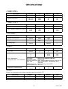
Page 4: Specifications
1-1 fl13.11sp specifications all items are measured across 8 Ω load at speaker output terminal with l.P.F. Description condition unit nominal limit 1. Aft pull-in range --- mhz ±2.3 ±2.1 2. Synchronizing sens. Tv.Ch.4 ca.Ch.31 ca.Ch.87 db μv db μv db μv 18 18 18 20 20 23 description condition unit n...
Page 5: Important Safety Precautions
2-1 ltvn_isp important safety precautions prior to shipment from the factory, our products are strictly inspected for recognized product safety and electrical codes of the countries in which they are to be sold. However, in order to maintain such compliance, it is equally important to implement the ...
Page 6
2-2 ltvn_isp 3. Design alteration warning - do not alter or add to the mechanical or electrical design of this tv receiver. Design alterations and additions, including, but not limited to circuit modifications and the addition of items such as auxiliary audio and/or video output connections, might a...
Page 7
2-3 ltvn_isp precautions during servicing a. Parts identified by the # symbol are critical for safety. Replace only with part number specified. B. In addition to safety, other parts and assemblies are specified for conformance with regulations applying to spurious radiation. These must also be repla...
Page 8
2-4 ltvn_isp safety check after servicing examine the area surrounding the repaired location for damage or deterioration. Observe that screws, parts and wires have been returned to original positions. Afterwards, perform the following tests and confirm the specified values in order to verify complia...
Page 9: Standard Notes For Servicing
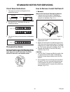
3-1 tvn_sn standard notes for servicing circuit board indications 1. The output pin of the 3 pin regulator ics is indicated as shown. 2. For other ics, pin 1 and every fifth pin are indicated as shown. 3. The 1st pin of every male connector is indicated as shown. Pb (lead) free solder pb free mark w...
Page 10
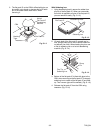
3-2 tvn_sn 3. The flat pack-ic on the cba is affixed with glue, so be careful not to break or damage the foil of each pin or the solder lands under the ic when removing it. With soldering iron: 1. Using desoldering braid, remove the solder from all pins of the flat pack-ic. When you use solder flux ...
Page 11
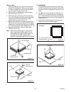
3-3 tvn_sn with iron wire: 1. Using desoldering braid, remove the solder from all pins of the flat pack-ic. When you use solder flux which is applied to all pins of the flat pack-ic, you can remove it easily. (fig. S-1-3) 2. Affix the wire to a workbench or solid mounting point, as shown in fig. S-1...
Page 12
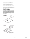
3-4 tvn_sn instructions for handling semi- conductors electrostatic breakdown of the semi-conductors may occur due to a potential difference caused by electrostatic charge during unpacking or repair work. 1. Ground for human body be sure to wear a grounding band (1 m Ω) that is properly grounded to ...
Page 13
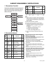
4-1 fl13.12_dc cabinet disassembly instructions 1. Disassembly flowchart this flowchart indicates the disassembly steps for the cabinet parts and the cba in order to gain access to items to be serviced. When reassembling, follow the steps in reverse order. Bend, route and dress the cables as they we...
Page 14
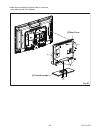
4-2 fl13.12_dc • make sure to replace the control plate to a new one when replacing the front cabinet. [1] stand assembly (s-2) [2] rear cover (s-1) (s-3) (s-3) fig. D1.
Page 15
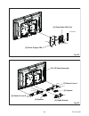
4-3 fl13.12_dc [3] power supply cba (s-5) [4] digital main cba unit (s-4) jack holder fig. D2 [5] stand bracket (s-6) [7] bottom cover l [6] speaker [8] bottom cover r (s-7) (s-8) (s-9) (s-10) [6] speaker [9] lcd panel assembly fig. D3.
Page 16
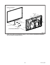
4-4 fl13.12_dc * 1 : make sure to read all the precautions on pages 4-1 and 4-2 when you disassemble/re-assemble the front cabinet or function cba unit. [11] function cba unit * 1 sensor lens *1 control plate *1 [10] front cabinet * 1 shield plate hook *1 (s-11) (s-11) (s-11) (s-11) blind label fig....
Page 17
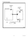
4-5 fl13.12_dc tv cable wiring diagram power supply cba function cba unit to lcd panel assembly to lcd panel assembly to ac cord to speaker digital main cba unit cn3801 cn4052 cn1001 cn601 cn501 cn3013 cn3101 cn3602 fig. D5.
Page 18
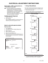
5-1 fl13.12ea electrical adjustment instructions general note: “cba” is abbreviation for “circuit board assembly.” note: electrical adjustments are required after replacing circuit components and certain mechanical parts. It is important to perform these adjustments only after all repairs and replac...
Page 19
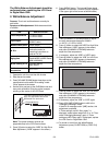
5-2 fl13.12ea the white balance adjustment should be performed when replacing the lcd panel or digital main cba. 2. White balance adjustment purpose: to mix red and blue beams correctly for pure white. Symptom of misadjustment: white becomes bluish or reddish. 1. Operate the unit for more than 60 mi...
Page 20
6-1 fl13.12_int how to initialize the lcd tv the purpose of initialization is to place the set in a new out of box condition. The customer will be prompted to select a language and program channels after the set has been initialized. To put the program back at the factory-default, initialize the lcd...
Page 21: Firmware Renewal Mode
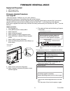
7-1 fl13.12fw firmware renewal mode equipment required a. Usb storage device b. Remote control unit firmware update procedure user upgrade (filename example: tvnb1012_00_ug_xx91_ba0.Bin) upgrade the firmware only. The setting values will not be initialized. The user upgrade and the firmware upgrade ...
Page 22
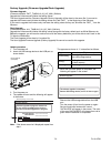
7-2 fl13.12fw factory upgrade (firmware upgrade/flash upgrade) firmware upgrade (filename example: fact_tvnb1012_00_ug_xx91_ba0.Bin) upgrade the firmware and initialize the setting values. The user upgrade and the firmware upgrade (factory upgrade) will be done by the same file. If you want to upgra...
Page 23: Troubleshooting
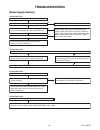
8-1 fl13.12atr troubleshooting [power supply section] the power cannot be turned on. The fuse blows out. Flow chart no.1 flow chart no.2 is normal state restored when once unplugged power cord is plugged again after several seconds? Check if there is any leak or short-circuit on the primary circuit ...
Page 24
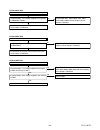
8-2 fl13.12atr no amp+13v is not output. Flow chart no.6 is approximately +12v voltage supplied to the cathode of d653(d655)? Yes check d653, d654, d655, c654, c655 and their periphery circuit. Repair it if defective. Check if there is any leak or short-circuit on the load circuit. Repair it if defe...
Page 25
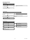
8-3 fl13.12atr [video signal section] no is the "l" pulse supplied to pin(5) of cn4052 when the remote control unit is activated? Yes is approximately +3.3v voltage supplied to pin(1) of cn4052? No flow chart no.2 check al+3.3v line and repair it if defective. Yes replace the digital main cba unit. ...
Page 26
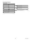
8-4 fl13.12atr [audio signal section] sp3801, sp3802 or cl3801 may be defective. Check and replace these parts. Audio is not output normally. Flow chart no.1 are the audio signals output to pin(1, 2, 3, 4) of cn3801? Replace the digital main cba unit. No yes is approximately +12v voltage supplied to...
Page 27: Block Diagrams
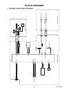
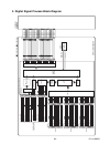
9-1 ic3001 (main micr o contr oller) digit al main cb a unit xout xin x3101 24mhz osc t o video/a udio block dia gram amp-mute amp-mute comp-det comp-det v ga-scl v ga-scl v ga-sd a v ga-sd a 194 195 67 212 127 133 213 66 cn3009 usb(+) usb(-) usb(+) usb(-) usb j a ck to led ba cklight drive block di...
Page 28
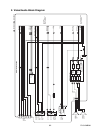
9-2 2. Video/audio block diagram fl13.12ablva digit al main cb a unit ic3801 (a udio amp) q3801 amp-mute comp-det t o system contr ol block dia gram sp3802 speaker r-ch cn3801 sp3801 speaker l-ch amp(l)-out amp(r)-out 3 sp(r)- 4 sp(r)+ 2 sp(l)- 1 sp(l)+ dif-out1 dif-out2 if-a gc t o digit al signal ...
Page 29
9-3 fl13.12abld digit al main cb a unit ic3001 (digit al signal pr ocess) cn3013 digit al signal pr ocess hdmi-in1 hdmi-in2 jk3003 d a t a0(+) d a t a0(-) d a t a1(+) d a t a1(-) d a t a2(+) d a t a2(-) hdmi-d a t a hdmi-clock 7 9 4 6 1 3 10 12 16 15 7 9 4 6 1 3 10 12 16 15 jk3002 clock(+) clock(-) ...
Page 30
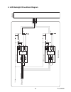
9-4 4. Led backlight drive block diagram ic1101 (led backlight driver) ov p drive q1101 contr ol logic 1 13 5 6 7 12 drive vreg fa il detect 11 17 15 vled1 1 iled1 2 q1102 po wer suppl y cb a lcd p anel assembl y pr o tect3 ba cklight -adj ba cklight -sw to system control block diagram p-on+21v cn10...
Page 31: Cold
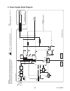
9-5 5. Power supply block diagram ho t cold po wer suppl y cb a hot circuit. Be careful. Q602 switching contr ol q621 o ver v o lt a ge pr o tect 1 4 3 2 t601 6 line fil ter l601 cn601 bridge rectifier d601- d604 4 5 12 11 10 9 8 7 1 q601 switching cn501 ic651 , q657 a c601 a c cord line fil ter l60...
Page 32
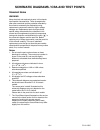
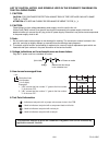
10-1 fl13.12sc schematic diagrams / cba and test points standard notes warning many electrical and mechanical parts in this chassis have special characteristics. These characteristics often pass unnoticed and the protection afforded by them cannot necessarily be obtained by using replacement compone...
Page 33
10-2 fl13.12sc list of caution, notes, and symbols used in the schematic diagrams on the following pages: 1. Caution: caution: for continued protection against risk of fire, replace only with same type_a,_v fuse. Attention: utiliser un fusible de rechange de mÊme type de_a,_v. 2. Caution: fixed volt...
Page 34
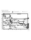
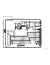
10-3 4 3 2 1 ic601 tlp781f open c603 l601 line filter ac601 ac cord 2.5a/250v f602 d653a open 1zb20bb d654 c654 470/16v 4.7k r663 open r664 c652 470/25v 1zb30bb d652 d650 sb3200bs 3.3k r661 3.9k r657 8.2k r667 2.7k r660 22k r659 180 r654 47k r668 10k r669 open c635 2200p/1kv c650 open d405 1 r651 d6...
Page 35
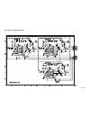
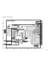
10-4 1/100v c1116 1/100v c1117 1k r1105 sk210td d1101 240k r1119 0 r1120 cn1001 1 vled1 2 iled1 1 c1103 1 c1104 100uh l1101 120 r1110 120 r1109 10 r1118 1ss400 d1103 47/100v c1113 47/100v c1112 open c1118 1 c1106 0.18/2w r1115 470/25v c1102 tfzvtr24b d1105 5.1k r1122 5.1k r1123 8 3 2 10 1 7 12 vcc u...
Page 36
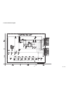
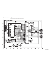
10-5 2 p-on+5v open c4055 6 key-in1 d4002 open 18k r4001 0.1 c4053 cn4052 1 al+3.3v sw4004 0.1 c4057 sw4005 10 c4051 r4055 open sw4006 3 light r4059 open 7 gnd 5 remote 4.7k r4003 sw4003 r4058 10k d4051 ltst-c190krkt 2.2k r4005 8.2k r4002 sw4002 r4056 10k 1000p c4052 1 2 3 4 5 6 ic4051 ph5502b2na1-e...
Page 37
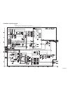
10-6 open r3045 open r3044 open r3047 open r3046 open c3057 p-on+21v vcom-pwm p-on+3.3v cell-pwr-ctrl open c3058 1 2 3 4 5 6 7 8 ic3201 mp1472gjc452z ss en comp fb gnd sw in bst 0.1 c3202 d3203 open 4.7 c3213 open c3210 4.7 c3211 open r3218 4.7 c3205 4.7 c3212 10k r3216 l3201 33uh 0.1 c3208 open c32...
Page 38
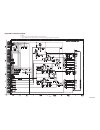
10-7 lvds-oclk(-) lvds-od0(+) lvds-od3(+) lvds-od2(-) lvds-od0(-) lvds-od2(+) lvds-od1(+) lvds-oclk(+) lvds-od3(-) lvds-od1(-) open r3931 open r3932 open r3933 open r3934 open r3935 4 cpv 17 gnd 11 llv4(+) 8 llv5(-) 28 gnd 26 pwr-ctrl 12 llv3(-) 1 stv 10 llv4(-) 13 llv3(+) 22 llv0(-) 29 lcd+12v 2 oe...
Page 39
10-8 ic3002 k4t51163qj-bce7 *a vdd j2 vref e2 nu k2 cke j8 ck k8 ck l8 cs k7 ras l7 cas k3 we l1 ba2/nu l3 ba1 l2 ba0 r2 a12 p7 a11 m2 a10/ap p3 a9 p8 a8 p2 a7 n7 a6 n3 a5 n8 a4 n2 a3 m7 a2 m3 a1 m8 a0 k9 odt *b vss a2 nu r8 a13 r7 nu r3 nu b7 udqs a8 udqs/nu b3 udm b9 mdqu7 c2 mdqu1 c8 mdqu0 f7 ldq...
Page 40
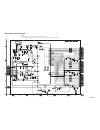
10-9 sp3801 speaker l-ch 3 sp(r)- 2 sp(l)- 4 sp(r)+ cn3801 1 sp(l)+ amp-mute al+3.3v p-on+5v amp+13v headphone jack jk3703 p-on+3.3v 1 2 3 4 27 28 26 25 22 24 23 21 6 5 8 7 10 11 12 9 13 14 18 20 15 19 16 17 control logic avcc power limit pwm logic drive gain control drive drive power limit pwm logi...
Page 41
10-10 6 p-on-h2 cn3601 1 led-cont(nu) 17 amp+13v 2 protect1 10 gnd 7 backlight-adj 11 gnd 15 amp+13v 14 gnd 21 p-on+21v 8 al+3.3v 22 p-on+21v 18 amp+13v 3 protect3 13 gnd 4 reset 23 p-on+21v 9 gnd 16 amp+13v 20 p-on+21v 12 gnd 5 backlight-sw 19 gnd 19 backlight-sw 21 protect3 8 amp+13v 2 p-on+21v 14...
Page 42
10-11 10k r3275 10k r3278 10k r3212 10k r3214 10k r3001 10k r3003 16 hdmi-data 12 clock(-) jk3004 1 data2(+) 6 data1(-) 3 data2(-) 14 arc 9 data0(-) 10 clock(+) 7 data0(+) 5 tmds data1 shield 17 gnd 18 +5v 13 hdmi-cec 15 hdmi-clock 19 hot plug detect 2 tmds data2 shield 4 data1(+) 11 tmds clock shie...
Page 43
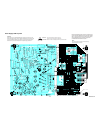
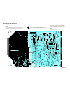
10-12 j132 gnd j134 gate1 j146 gnd js603 +b j71 p-on+21v j73 amp+13v j78 gnd j102 vled2 j136 gate3 uvlo1 protect3 gate2 protect3 isen2 ovp3 j126 bl-adj j138 isen3 j143 tc54_1 j144 ovp2 j150 gate2 j157 gnd j160 cs2 j162 gate3 j167 dimout3 j168 bl-sw r678 r679 c663 j602 j603 all-3.3v j87 amp+13v j88 a...
Page 44
10-13 t 2.5a l/250v ba3at0f0102 2 j126 bl-adj j127 q657 j128 gnd c1312 c1313 j130 j131 r601 j132 gnd r602 j133 j134 gate1 r605 j137 j138 isen3 r610 r611 j143 tc54_1 j144 ovp2 j146 gnd r619 r1115 cn601 j150 gate2 j151 r1315 j157 gnd l1201 j160 cs2 j162 gate3 j166 iled3 j167 dimout3 j168 bl-sw c602 c6...
Page 45: Wiring Diagram
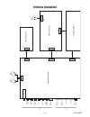
Fl13.12awi 11-1 wiring diagram 1 23 cn3602 1 51 cn3013 1 9 cn3101 digit al main cb a unit 14 cn3801 sp3801 speaker l-ch sp3802 speaker r-ch cl3801 tuner unit component -y/video-in component -pb-in component -pr-in audio(l)-in audio(r)-in rear digital audio-out (coaxial) hdmi- connector-1 hdmi- conne...
Page 46
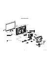
12-1 fl13.12-a_cex exploded views ssk1 sa1 see electrical parts list for parts with this mark. S7 a15 l24 l7 x6 b17 b18 a3 l23 b19 l35 l23 b23 l23 a13 a4-1 a4-2 l7 l7 l23 l23 b10 s7 a1 a16 b12 a9 a6 l7 l7 b18 b17 l7 l7 a21 function cba unit sp3801 sp3802 cl3801 cl3012 cl3101 l23 l7 power supply cba ...
Page 47
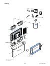
12-2 fl13.12-a_pex packing packing tape packing tape some ref. Numbers are not in sequence. S7 s4 s1 s8 s3 ssk1 x1 x4 x3 x12 x2 s7 x7 sa1 tape s3 x22 rear side rear side s6.
Page 48: Mechanical Parts
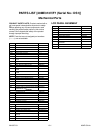
2013/07/19 13-1 a3ap1ca.Fm parts list [40me313v/f7 (serial no.: ds1)] mechanical parts product safety note: products marked with a # have special characteristics important to safety. Before replacing any of these components, read carefully the product safety notice in this service manual. Don't degr...
Page 49: Electrical Parts
2013/07/19 13-2 a3ap1el.Fm electrical parts product safety note: products marked with a # have special characteristics important to safety. Before replacing any of these components, read carefully the product safety notice in this service manual. Don't degrade the safety of the product through impro...
Page 50
2013/07/19 13-3 a3ap1el.Fm d661 switching diode 1ss400 te61 qd1z001ss400 d1101 diode schottky smd sk210td nd1z0sk210td d1103 switching diode 1ss400 te61 qd1z001ss400 d1104 switching diode 1ss400 te61 qd1z001ss400 d1105 zener diode smd tfzvtr24b qd1b00tfzv24 d1301 diode schottky smd sk210td nd1z0sk21...
Page 51
2013/07/19 13-4 a3ap1el.Fm r1321 res chip 1608 1/10w f 10.0k Ω rtw1002hh008 r1322 res chip 3216 1/4w j 5.1k Ω rrx4512hh034 r1323 res chip 3216 1/4w j 5.1k Ω rrx4512hh034 r1324 res chip 1608 1/10w j 1.0k Ω rrxa102hh013 r1325 res chip 1608 1/10w j 51 Ω rrxa510hh013 r1326 res chip 3216 1/4w f 1.00 Ω rt...
Page 52: Revision History
14-1 fl13.12rev revision history chassis fl13.12 • 2013/8/5 40me313v/f7 (serial no.: ds1) 1st draft added.
Page 53
Comparison list of model names chassis fl13.12 40me313v/f7 (ds1) a3ap1uh.

