- DL manuals
- Magnavox
- DVD Player
- sylvania DVC840F
- Service manual
Magnavox sylvania DVC840F Service manual
SERVICE MANUAL
Main Section
I
Specifications
I
Preparation for Servicing
I
Adjustment Procedures
I
Schematic Diagrams
I
CBA’s
I
Exploded Views
I
Parts List
When servicing the deck
mechanism, refer to MK14 Deck
Mechanism Section.
Deck Mechanism Part No.:
N2440FL, N2460FL
DVD PLAYER &
VIDEO CASSETTE RECORDER
DVC840F
MWD2205
DVC865F
Summary of sylvania DVC840F
Page 1
Service manual main section i specifications i preparation for servicing i adjustment procedures i schematic diagrams i cba’s i exploded views i parts list when servicing the deck mechanism, refer to mk14 deck mechanism section. Deck mechanism part no.: n2440fl, n2460fl dvd player & video cassette r...
Page 2: Important Safety Notice
Important safety notice proper service and repair is important to the safe, reliable operation of all funai equipment. The service procedures recommended by funai and described in this service manual are effective methods of performing service operations. Some of these service special tools should b...
Page 3: Main Section
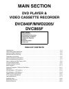
Main section dvd player & video cassette recorder dvc840f/mwd2205/ dvc865f table of contents specifications . . . . . . . . . . . . . . . . . . . . . . . . . . . . . . . . . . . . . . . . . . . . . . . . . . . . . . . . . . . . . . . . . . . . . . . . . . 1-1-1 laser beam safety precautions . . . . ...
Page 4: Specifications
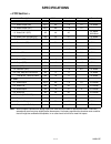
1-1-1 h9801sp specifications note: nominal specs represent the design specs. All units should be able to approximate these – some will exceed and some may drop slightly below these specs. Limit specs represent the absolute worst condition that still might be considered acceptable; in no case should ...
Page 5
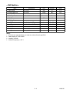
1-1-2 h9801sp notes: 1. All items are measured without pre-emphasis unless otherwise specified. 2. Power supply: ac 120 v, 60 hz 3. Load imp.: 100 k Ω 4. Ambient temperature: +25 °c item conditions unit nominal limit 1. Video output 75 Ω load vpp 1.0 ± 0.1 2. Coaxial digital out 75 Ω load mvpp 500 ±...
Page 6
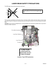
1-2-1 e6nlsp laser beam safety precautions this dvd player uses a pickup that emits a laser beam. The laser beam is emitted from the location shown in the figure. When checking the laser diode, be sure to keep your eyes at least 30 cm away from the pickup lens when the diode is turned on. Do not loo...
Page 7: Important Safety Precautions
1-3-1 dvdn_isp important safety precautions product safety notice some electrical and mechanical parts have special safety-related characteristics which are often not evident from visual inspection, nor can the protection they give necessarily be obtained by replacing them with components rated for ...
Page 8
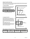
1-3-2 dvdn_isp safety check after servicing examine the area surrounding the repaired location for damage or deterioration. Observe that screws, parts, and wires have been returned to their original positions. Afterwards, do the following tests and confirm the specified values to verify compliance w...
Page 9: Standard Notes For Servicing
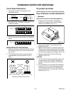
1-4-1 dvdn_sn standard notes for servicing circuit board indications 1. The output pin of the 3 pin regulator ics is indicated as shown. 2. For other ics, pin 1 and every fifth pin are indicated as shown. 3. The 1st pin of every male connector is indicated as shown. Instructions for connectors 1. Wh...
Page 10
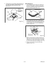
1-4-2 dvdn_sn 3. The flat pack-ic on the cba is affixed with glue, so be careful not to break or damage the foil of each pin or the solder lands under the ic when removing it. With soldering iron: 1. Using desoldering braid, remove the solder from all pins of the flat pack-ic. When you use solder fl...
Page 11
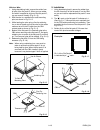
1-4-3 dvdn_sn with iron wire: 1. Using desoldering braid, remove the solder from all pins of the flat pack-ic. When you use solder flux which is applied to all pins of the flat pack-ic, you can remove it easily. (fig. S-1-3) 2. Affix the wire to a workbench or solid mounting point, as shown in fig. ...
Page 12
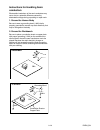
1-4-4 dvdn_sn instructions for handling semi- conductors electrostatic breakdown of the semi-conductors may occur due to a potential difference caused by electrostatic charge during unpacking or repair work. 1. Ground for human body be sure to wear a grounding band (1 m Ω) that is properly grounded ...
Page 13: Preparation For Servicing
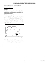
1-5-1 h9801pfs preparation for servicing how to enter the service mode about optical sensors caution: an optical sensor system is used for the tape start and end sensors on this equipment. Carefully read and follow the instructions below. Otherwise the unit may operate erratically. What to do for pr...
Page 14
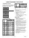
1-6-1 h9801dc cabinet disassembly instructions 1. Disassembly flowchart this flowchart indicates the disassembly steps to gain access to item(s) to be serviced. When reassembling, follow the steps in reverse order. Bend, route, and dress the cables as they were originally. 2. Disassembly method note...
Page 15
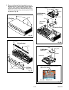
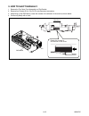
1-6-2 h9801dc 5. Before installing the deck assembly, be sure to place the pin of ld-sw on main cba as shown in fig. D6. Then, install the deck assembly while aligning the hole of cam gear with the pin of ld- sw, the shaft of cam gear with the hole of ld-sw as shown in fig. D6. (s-1) [1] top case fi...
Page 16
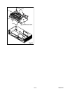
1-6-3 h9801dc fig. D5 (s-7) (s-7) (s-7) (s-8) [8] vcr chassis unit.
Page 17
1-6-4 h9801dc fig. D6 (s-9) (s-10) (s-11) [11] main cba [9] deck assembly [10] dvd open/close cba fe head cylinder assembly ace head assembly desolder lead with blue stripe from fe head bottom view lead connections of deck assembly and main cba desolder from capstan motor assembly printing side deso...
Page 18
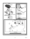
1-6-5 h9801dc 3. How to eject manually 1. Remove the top case, front assembly and top bracket. 2. Remove four screws (s-3) in fig. D3. Do not disconnect connectors. 3. While lifting up the dvd mecha, rotate the roulette in the direction of the arrow as shown below. 4. Pull the tray slowly with a han...
Page 19
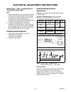
1-7-1 h9801ea electrical adjustment instructions general note: “cba” is abbreviation for “circuit board assembly.” note: 1. Electrical adjustments are required after replacing circuit components and certain mechanical parts. It is important to do these adjustments only after all repairs and replacem...
Page 20
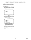
1-8-1 h9801int how to initialize the dvd player & vcr to put the program back at the factory-default, initialize the dvd player & vcr as the following procedure. 1. Press [dvd], [1], [2], [3], [4], and [display] buttons on the remote control unit in that order. Fig. A appears on the screen. 2. Press...
Page 21: Firmware Renewal Mode
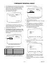
1-9-1 h9801fw firmware renewal mode 1. Turn the power on and remove the disc on the tray. 2. To put the dvd player into version up mode, press [dvd], [9], [8], [7], [6], and [search mode] buttons on the remote control unit in that order. The tray will open automatically. Fig. A appears on the screen...
Page 22: Function Indicator Symbols
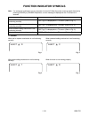
1-10-1 h9801fis function indicator symbols note: if a mechanical malfunction occurs, the power is turned off. When the power comes on again after that by pressing [power] or [standby-on] button, an error message is displayed on the tv screen for 5 seconds. Tv screen when reel or capstan mechanism is...
Page 23: Block Diagrams
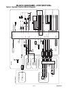
1-11-1 block diagrams servo / system control block diagram m loading motor sensor cba sensor cba capstan motor contr ol head cn502 cn504 ac head assembly main cba key- 2 rf-sw c-fg c-cont d-pfg st-s t-reel c-f/r key- 1 d-v sync c-sync v-env ctl(+) reset c-rota d-rec-h d-rec-h rec- saf-sw pg-delay au...
Page 24
1-11-2 video block diagram main cb a q391 tu701 video in vcr dvd output-select video out tp751 v-out 6 18 rec video signal pb video signal d v d video signal mode: sp/rec wf1 buffer sw ctl ic751 (output select) 15 1 2 9 10 11 to servo/system control block diagram dvd-video to dvd video/audio block d...
Page 25
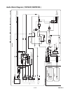
1-11-3 audio block diagram ( dvc840f, mwd2205 ) tu701 a udio out a udio in rec amp serial i/f 9 8 au t o bias 11 p-on+5v p-on+5v q421 bias osc q422 q426 (pb=on) q425 switching d-rec off 6 eq amp line amp mute lpf 10 sp/lp-on p r alc (a udio pr ocess) 76 80 78 tuner line 1 line 2 2 14 4 a u dio-pb/re...
Page 26
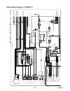
1-11-4 audio block diagram ( dvc865f ) tu701 sif out a udio in rec amp serial i/f 9 8 au t o bias 11 p-on+5v p-on+5v q421 bias osc q422 q426 (pb=on) q425 switching d-rec off 6 eq amp line amp mute lpf 10 sp/lp-on p r alc (a udio pr ocess) 76 80 78 tuner line 1 line 2 2 15 4 a u dio-pb/rec cn504 3 a-...
Page 27
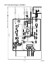
1-11-5 hi-fi audio block diagram ( dvc865f ) 57 48 47 13 14 69 71 6 7 9 r-ch insel l-ch insel nor sw serial data decoder output select vco lpf l-ch bpf r-ch pnr pilot det cont stereo pll stereo filter sap filter sap det sif demod sap demod l-r demod st/sap sw matrix l-ch pnr lim dev comp sw noise vc...
Page 28: Cold
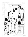
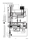
1-11-6 power supply block diagram ac1001 f1001 1a 250v line filter l1001 d1001 - d1004 bridge rectifier 2 4 q1001 q1003 q1008 8 7 1 2 3 4 ic1001 error voltage det t001 q055 q052 q056 main cba hot circuit. Be careful. 20 19 18 17 16 15 14 13 12 11 q1006 q1005 q1011 q031 1 ev+1.2v 2 ev+1.2v 3 ev+3.3v ...
Page 29: Block Diagrams
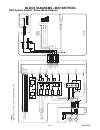
1-11-7 block diagrams h9801blsd dvd system control / servo block diagram remo te sensor rm2001 remo te-video main cb a 20 21 21 22 19 20 18 19 remo t e 2 2 dv d-open/close 24 23 t o ser v o/system contr o l block dia gram d v d-po wer cn401 cn1001 d v d-pla y 2 5 26 d v d-st op 26 27 d vd-po wer 23 ...
Page 30
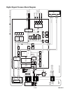
1-11-8 h9801bld digital signal process block diagram d a t a (video/a udio) signal d v d video signal d a t a(a udio) signal c1 6 d1 8 a1 7 b1 5 e1 4 f1 2 d vd-ld 8 cd-ld 10 pd-moni 7 fs(+) 2 fs(-) 3 ts(+) 1 ts(-) 4 cn201 cn201 cn201 ic201 (sw) ic501, ic502 (sdram) ic101 (micr o contr oller) fs fs(+...
Page 31
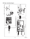
1-11-9 h9801blvd dvd video / audio block diagram ic601 (a udio d a c) 15 14 16 digit al a udio out jk1202 b uffer q1351 ic1201 q1201 q1202 +5v (amp) cn601 cn1601 13 13 d v d-a udio(l) 15 15 d v d-a udio(r) 14 14 dvd-a udio(r)-mute 7 6 8 4 3 2 5 t o d vd system contr ol /ser v o block dia gram t o di...
Page 32
1-12-1 d6n_sc schematic diagrams / cba’s and test points standard notes warning many electrical and mechanical parts in this chassis have special characteristics. These characteristics often pass unnoticed and the protection afforded by them cannot necessarily be obtained by using replacement compon...
Page 33
1-12-2 d6n_sc list of caution, notes, and symbols used in the schematic diagrams on the following pages: 1. Caution: for continued protection against fire hazard, replace only with the same type fuse. Attention: pour une protection continue les risqes d'incele n'utiliser que des fusible de mÊme type...
Page 34
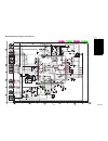
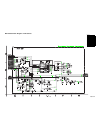
1-12-3 main 1/8 schematic diagram h9801scm1 main 1/8 ref no. Position ic501 c-3 q501 d-1 q506 a-2 cn501 a-4 cn502 f-4 cn504 a-4 vr501 b-4 tp505 b-2 tp513 b-4 ic connectors test points variable resistor transistors.
Page 35
1-12-4 main 2/8 & sensor schematic diagram h9801scm2 main 2/8 ref no. Position q563 h-3 q565 h-3 q566 h-2 q567 i-2 tp502 i-4 tp506 k-1 tp507 k-1 test points transistors.
Page 36
1-12-5 main 3/8 schematic diagram h9801scm3 main 3/8 ref no. Position ic301 o-2 q301 q-3 q302 q-4 q303 q-4 q421 n-1 q422 n-1 q425 n-1 q426 n-1 cn253 m-4 tp301 p-1 tp302 o-4 connector test points ic transistors.
Page 37
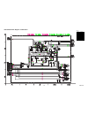
1-12-6 main 4/8 schematic diagram h9801scm4 main 4/8 ref no. Position ic1201 t-1 ic1402 u-3 q1201 u-1 q1202 u-1 q1204 u-1 q1351 v-1 q1385 s-2 cn1601 s-3 connector transistors ics.
Page 38
1-12-7 main 5/8 schematic diagram h9801scm5 main 5/8 ref no. Position ic751 z-3 q391 aa-3 q762 z-2 q763 z-2 tp751 aa-2 tp753 aa-2 tp754 aa-2 ic transistors test points.
Page 39
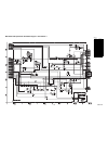
1-12-8 main 6/8 & dvd open/close schematic diagram h9801scm6 main 6/8 ref no. Position ic1002 ad-4 ic1004 ad-3 q052 ag-4 q055 af-3 q056 ag-3 q057 ae-3 q1004 ae-2 q1005 af-2 q1006 ag-2 q1011 ad-2 q2002 af-1 q2013 ad-1 cn1001 ac-3 cn2003 ag-1 connectors transistors ics.
Page 40
1-12-9 main 7/8 schematic diagram h9801scm7 caution ! Fixed voltage ( or auto voltage selectable ) power supply circuit is used in this unit. If main fuse(f1001)is blown , check to see that all components in the power supply circuit are not defective before you connect the ac plug to the ac power su...
Page 41
1-12-10 h9802scm8 main 8/8 schematic diagram ( dvc865f ).
Page 42
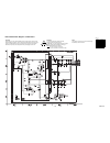
1-12-11 h9801scd1 dvd main 1/3 schematic diagram dvd main 1/3 ref no. Position ic201 c-1 ic202 d-4 ic301 d-3 ic461 f-1 ic462 e-1 q251 c-2 q252 b-2 q253 c-2 q254 b-2 cn201 a-3 cn301 a-1 cn401 f-3 transistors connectors ics 1 note: either ic461 or ic462 is used for dvd main cba unit..
Page 43
1-12-12 h9801scd2 dvd main 2/3 schematic diagram dvd main 2/3 ref no. Position ic101 h-4 cn702 g-2 ic connector.
Page 44
1-12-13 ic101 voltage chart pin.No play stop pin.No play stop pin.No play stop pin.No play stop 1 ~ ~ 33 ~ ~ 65 0 0 97 ----- ----- 2 ~ ~ 34 3.4 3.4 66 3.4 3.5 98 3.4 3.4 3 0 0 35 0 0 67 3.2 3.2 99 0.9 0.8 4 ~ ~ 36 ~ ~ 68 0 0 100 0 0 5 ~ ~ 37 ~ ~ 69 ----- ----- 101 2.4 2.4 6 3.4 3.4 38 0.4 0.3 70 3.4...
Page 45
1-12-14 h9801scd3 dvd main 3/3 schematic diagram dvd main 3/3 ref no. Position ic103 n-3 ic501 o-4 ic502 q-4 ic601 p-1 cn601 r-1 ics connector.
Page 46
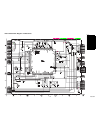
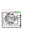
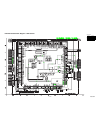
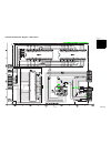
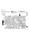
1-12-15 to sensor cba (start-sensor) v-out tp751 wf1 s-inh tp502 to sensor cba (end-sensor) bh9800f01011a main cba top view bh9800f01011c dvd open/close cba top view caution ! Fixed voltage ( or auto voltage selectable ) power supply circuit is used in this unit. If main fuse(f1001)is blown , check ...
Page 47
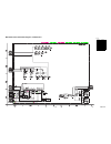
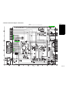
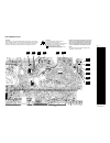
1-12-16 pin 2 of tu701 wf10 pin 6 of tu701 wf11 pin 11 of tu701 wf12 pin 12 of tu701 wf13 pin 14 of tu701 wf14 pin 18 of tu701 wf15 pin 8 of cn1601 pin 18 of cn1601 pin 13 of cn1601 pin 10 of cn1601 pin 15 of cn1601 wf6 wf5 wf4 wf8 wf7 wf6 wf7 wf5 wf4 wf8 wf9 pin 2 of ic751 main cba bottom view bh98...
Page 48: Waveforms
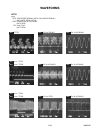
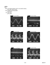
Waveforms wf1 wf3 wf1 upper wf2 wf2 lower tp751 tp751 tp302 upper lower tp302 tp301 wf4 wf6 pin 2 of ic751 wf5 video-y video-y 0.2v 0.2v 20 20 µs video-c video-c 0.2v 0.2v 20 20 µs video-cvbs video-cvbs 0.5v 0.5v 20 20 µs s wf7 audio-l audio-l 1v 1v 0.5ms 0.5ms wf8 audio-r audio-r 1v 1v wf9 spdif sp...
Page 49
Wf13 wf11 wf12 wf10 wf14 wf15 pin 2 of tu701 pin 14 of tu701 pin 12 of tu701 pin 11 of tu701 pin 6 of tu701 pin 18 of tu701 note: input vcr: color bar signal (with 1khz audio signal) (wf1~wf3, wf10~wf15) dvd: power on (stop) mode (wf4~wf6) cd: 1khz play (wf7~wf9) mod-a 0.5v 0.2ms mod-v 0.5v 20 µs pl...
Page 50: Wiring Diagram
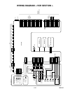
Wiring diagram ac head assembly audio head audio erase head control head m loading motor cylinder assembly ae-h 1 ae-h/fe-h 2 a-com 3 audio-pb/rec 4 ctl(+) 5 ctl(-) 6 hi-fi-audio(r) 7 hi-fi-com 8 hi-fi-audio(l) 9 video-com 5 video(r)-2 6 video(r)-1 1 video-com 2 video(l)-2 3 video(l)-1 4 p-on+5v 1 a...
Page 51: Wiring Diagram
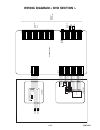
Wiring diagram dvd mecha dvd main cba unit to wiring diagram to main cba cn1001 to main cba cn1601 cn301 3 4 tra y -in gnd sl(-) 5 6 sp(-) 7 sp(+) 8 sl(+) tray-in drive cba m sled motor m spindle motor ev+1.2v ev+1.2v ev+3.3v ev+3.3v ev+3.3v dvd-p-on+3.3v dvd-p-on+5v ev+10v ev+10v gnd 2 3 4 5 6 7 8 ...
Page 52
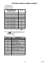
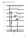
1-15-1 d6n4hti system control timing charts mode sw: ld-sw note: ej rs: loading fwd (lm-fwd / rev “h”) rs ej: loading rev (lm-fwd / rev “l”) stop (a) = loading stop (b) = unloading note: ld-sw position detection a/d input voltage limit (calculated voltage) symbol 3.76 v ~ 4.50 v (4.12 v) ej 4.51 v ~...
Page 53
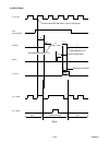
1-15-2 d6n4hti still/slow control frame advance timing chart 1) sp mode fig. 1 18 rf-sw f-ad (internal signal) c-drive pb ctl 27 c-f/r 79 h-a-sw 78 c-rota the first rise of rf-sw after a rise in f-ad signal acceleration detection (t1) at "h" "z" "h" "l" "l" stop detection (t2) st slow tracking value...
Page 54
1-15-3 d6n4hti 2) lp/slp mode fig. 2 18 rf-sw f-ad (internal signal) c-drive pb ctl 27 c-f/r 79 h-a-sw 78 c-rota "h" "z" "h" "l" "l" still still at st bl stop detection (t2) acceleration detection (t1) slow tracking value reversal limit value frame advance the first rise of rf-sw after a rise in f-a...
Page 55
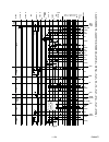
1-15-4 d6n4hti fig. 3 1. Eject (po w er off) -> cassette in (po wer on) -> st op(b) -> st op(a) -> pla y -> rs -> fs -> pla y -> still -> pla y -> st op(a) eject cass.Load st-s/ end-s "off" play rew ff play play stop /eject 0.2s 0.7s 0.4s 0.2s ld-fwd stop(a) stop(a) ld-fwd ld-rev 0.2s ld-fwd ld-fwd ...
Page 56
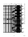
1-15-5 d6n4hti fig. 4 pin no . Ld-sw cl/ss lm-fwd "m" /rev c-drive "z" on on c-f/r dr um r o t a tion p-on-l a-mute-h d-rec-h d-pb ej au rs sf sm tl fb al sb 68 21 27 22 7 24 vcr/tv 77 displa y st-s/ end-s "on" rec rew ff stop /eject 0.5s 1.0s 0.2s 0.5s 0.2s 0.5s 0.5s 0.5s 0.2s 0.2s 0.2s 1.5s 2.5s s...
Page 57
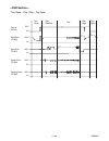
1-15-6 d6n4hti tray in (tl221) sled drive (tp303) disc drive (tp301) focus drive (tp304) tracking drive (tp302) 0v 3.3v 0v 1.65v 0v 0v 0v 1.65v 1.65v 1.65v tray close ~ play / play ~ tray open tray close disc rotation play disc stop tray open.
Page 58
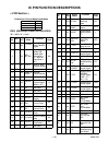
1-16-1 h9801pin ic pin function descriptions comparison chart of models and marks ic501 (servo/system control/osd) “h” ≥ 4.5 v, “l” ≤ 1.0 v model mark dvc840f a mwd2205 b dvc865f c pin no. Mark in/ out signal name function active level 1 in p-down -l power voltage down detector signal l 2 in rec- sa...
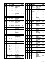
Page 59
1-16-2 h9801pin 38 out video- out composite video signal output - 39 - vss2 vss2 - 40 in video-in composite video signal input - 41 in c-sync composite synchronized pulse pulse 42 - vdd2 vdd2 - 43 in afcc low path filter input signal for afc - 44 out afclpf low path filter output signal for afc - 45...
Page 60
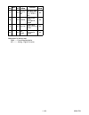
1-16-3 h9801pin notes: abbreviation for active level: pwm ----- pulse wide modulation a/d -------- analog - digital converter 77 out vcr/tv- ind rf conv. On/ off signal (tv = “l” / vcr = “h”) h/l 78 out c-rota color phase rotary changeover signal h/l 79 out h-a-sw video head amp switching pulse h/l ...
Page 61: Lead Identifications
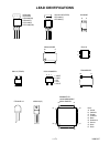
1-17-1 h9801le lead identifications 60 21 40 41 20 1 80 61 e c b e c b a k c e 1 4 8 5 16 9 8 1 e c b1 e b2 c1 c2 4 5 3 1 2 pq1lax95mspq 1: vref 2: gnd 3: vc 4: vin 5: vout ba5888fp-e2 la72670bm-mpb-e mn101d08dek note: a: anode k: cathode e: emitter c: collector b: base r: reference s: source g: gat...
Page 62
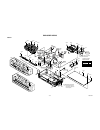
1-18-1 h9801cex exploded views cabinet a22 a22 2b2 2l051 2l051 2l051 2b3 2l011 2l012 1b1 2l071 2l071 2l071 2l071 a2 2l041 2l041 2l041 2l041 2b40 2l022 2l022 2l021 2l021 2l021 1b2 l0-9 l0-9 dvd main cba unit sensor cba sensor cba a4 a5 ac1001 2b11 2b15 2b15 rm2001 dvd open/close cba w002 w011 2l091 2...
Page 63
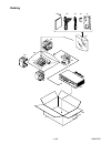
1-18-2 h9801pex packing s2 s2 s2 s2 s1 unit a14 s3 x1 x4 x20 x5 x2 x3.
Page 64: Mechanical Parts List
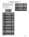
20050114 1-19-1 h9801ca mechanical parts list product safety note: products marked with a # have special characteristics important to safety. Before replacing any of these components, read carefully the product safety notice in this service manual. Don't degrade the safety of the product through imp...
Page 65: Electrical Parts List
20050114 1-20-1 h9801el electrical parts list product safety note: products marked with a # have special characteristics important to safety. Before replacing any of these components, read carefully the product safety notice in this service manual. Don't degrade the safety of the product through imp...
Page 66
20050114 1-20-2 h9801el c455 c electrolytic cap. 22 µf/6.3v m h7 ce0kmavsl220 c456 c electrolytic cap. 10 µf/16v m h7 ce1cmavsl100 c457 c electrolytic cap. 4.7 µf/25v m h7 ce1emavsl4r7 c458 c chip ceramic cap. B k 0.01 µf/50v chd1jkb0b103 c459 c electrolytic cap. 22 µf/6.3v m h7 ce0kmavsl220 c460 c ...
Page 67
20050114 1-20-3 h9801el c1394 electrolytic cap. 47 µf/6.3v m h7 ce0kmassl470 c1395 electrolytic cap. 470 µf/6.3v m ce0kmasdl471 c1421 chip ceramic cap. B k 0.01 µf/50v chd1jkb0b103 c1422 chip ceramic cap. B k 0.1 µf/25v chd1ekb0b104 c1441 chip ceramic cap. B k 0.33 µf/10v chd1akb0b334 c1442 electrol...
Page 68
20050114 1-20-4 h9801el q1004 transistor ktc3203(y) nqsy0ktc3203 q1005 transistor ktc3199(y) nqsy0ktc3199 q1006 transistor kta1267(y) nqsy0kta1267 q1008 transistor ktc3199(y) nqsy0ktc3199 q1011 transistor ktc3203(y) nqsy0ktc3203 q1201 transistor ktc3199(y) nqsy0ktc3199 q1202 transistor ktc3199(y) nq...
Page 69
20050114 1-20-5 h9801el r527 chip res.(1608) 1/10w j 1k Ω rrxajb5z0102 r528 carbon res. 1/4w j 10k Ω rcx4jatz0103 r530 carbon res. 1/4w j 1k Ω rcx4jatz0102 r531 carbon res. 1/6w g 4.7k Ω rcx6gatz0472 r532 carbon res. 1/6w g 1.5k Ω rcx6gatz0152 r533 carbon res. 1/6w g 22k Ω rcx6gatz0223 r534 carbon r...
Page 70
20050114 1-20-6 h9801el dvd open/close cba sensor cba r1461 chip res.(1608) 1/10w f 75 Ω rrxafb5h75r0 r1462 chip res.(1608) 1/10w j 75 Ω rrxajb5z0750 r1481 chip res.(1608) 1/10w f 75 Ω rrxafb5h75r0 r1482 chip res.(1608) 1/10w j 75 Ω rrxajb5z0750 r1490 chip res.(1608) 1/10w 0 Ω rrxazb5z0000 r1521 b c...
Page 71
Dvc840f/mwd2205/dvc865f h9801ud/h98k0ud/h9802ud 2005-01-28.

