- DL manuals
- N.A.T.
- Switch
- NAT-MCH
- Technical Reference
N.A.T. NAT-MCH Technical Reference
Summary of NAT-MCH
Page 1
Nat-mch clock-module – technical reference manual nat-mch clock-module technical reference manual v 1.4 clk module hw revision 2.1 and revision 2.3.
Page 2: N.A.T. Gmbh
Nat-mch clock-pcb – technical reference manual version 1.4 © n.A.T. Gmbh 2 the nat-mch has been designed by: n.A.T. Gmbh kamillenweg 22 d-53757 sankt augustin phone: ++49/2241/3989-0 fax: ++49/2241/3989-10 e-mail: support@nateurope.Com internet: http://www.Nateurope.Com.
Page 3: Disclaimer
Nat-mch clock-pcb – technical reference manual version 1.4 © n.A.T. Gmbh 3 disclaimer the following documentation, compiled by n.A.T. Gmbh (henceforth called n.A.T.), repre- sents the current status of the product’s development. The documentation is updated on a regular basis. Any changes which migh...
Page 4: Table of Contents
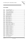
Nat-mch clock-pcb – technical reference manual version 1.4 © n.A.T. Gmbh 4 table of contents conventions................................................................................................................................................... 8 1 board specification ...........................
Page 5: List of Figures
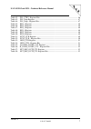
Nat-mch clock-pcb – technical reference manual version 1.4 © n.A.T. Gmbh 5 11.3.7 source selection 1 register ...................................................................................................... 33 11.3.8 source selection 2 register ....................................................
Page 6: List of Tables
Nat-mch clock-pcb – technical reference manual version 1.4 © n.A.T. Gmbh 6 list of tables table 1: list of used abbreviations ..................................................................................... 8 table 2: nat-mch clk module features ....................................................
Page 7
Nat-mch clock-pcb – technical reference manual version 1.4 © n.A.T. Gmbh 7 table 42: pll_ctr2 - register bits ................................................................................... 46 table 43: pll_outp register ..............................................................................
Page 8: Conventions
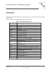
Nat-mch clock-pcb – technical reference manual version 1.4 © n.A.T. Gmbh 8 conventions if not otherwise specified, addresses and memory maps are written in hexadecimal notation, identified by 0x. Table 1: gives a list of the abbreviations used in this document: table 1: list of used abbreviations ab...
Page 9: 1 Board
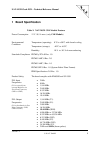
Nat-mch clock-pcb – technical reference manual version 1.4 © n.A.T. Gmbh 9 1 board specification table 2: nat-mch clk module features power consumption 12 v / 0.5 a max. (only clk module) environmental conditions temperature (operating): temperature (storage): humidity: 0°c to +50°c with forced cool...
Page 10
Nat-mch clock-pcb – technical reference manual version 1.4 © n.A.T. Gmbh 10 2 statement on environmental protection 2.1 compliance to rohs directive directive 2002/95/ec of the european commission on the "restriction of the use of certain hazardous substances in electrical and electronic equipment" ...
Page 11
Nat-mch clock-pcb – technical reference manual version 1.4 © n.A.T. Gmbh 11 as n.A.T. Products are solely sold to industrial customers, by special arrangement at time of purchase the customer agreed to take the responsibility for a weee compliant disposal of the used n.A.T. Product. Moreover, all n....
Page 12: 3 Installation
Nat-mch clock-pcb – technical reference manual version 1.4 © n.A.T. Gmbh 12 3 installation 3.1 safety note to ensure proper functioning of the nat-mch clk module during its usual lifetime take refer to the safety note section of the nat-mch basic- module technical reference manual before handling th...
Page 13: 4 Introduction
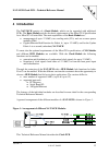
Nat-mch clock-pcb – technical reference manual version 1.4 © n.A.T. Gmbh 13 4 introduction the nat-mch consists of a basic-module, which can be expanded with additional pcbs. The basic-module satisfies the basic requirements of the microtca specification for a microtca carrier hub. The main capabili...
Page 14: 5 Clk Module Basics
Nat-mch clock-pcb – technical reference manual version 1.4 © n.A.T. Gmbh 14 5 clk module basics the clk module can be mounted on the nat-mch basic-pcb. With the clk module, the 2 nd tongue of the nat-mch connector to the microtca backplane is installed. The nat-mch clk module implements the followin...
Page 15
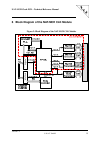
Nat-mch clock-pcb – technical reference manual version 1.4 © n.A.T. Gmbh 15 6 block diagram of the nat-mch clk module figure 2: block diagram of the nat-mch clk module ba ck pl an e c onn ec tor conn ec tor to ba si c-p c b conn ec tor to pcie hub-pcb.
Page 16: 7 Board Features
Nat-mch clock-pcb – technical reference manual version 1.4 © n.A.T. Gmbh 16 7 board features • pll the board is equipped with a zarlink zl30105 stratum 3 pll, which provides various typical telecom frequencies in the range from 8 khz to 65.536 mhz. Especially to the two frequencies 8 khz and 19.44 m...
Page 17
Nat-mch clock-pcb – technical reference manual version 1.4 © n.A.T. Gmbh 17 • interface to other nat-mch pcbs basic pcb: - the microprocessor on the clk module can be programmed by the coldfire on the basic-module via a spi interface. Normal communication between the microprocessor and the coldfire ...
Page 18: 8 Functional
Nat-mch clock-pcb – technical reference manual version 1.4 © n.A.T. Gmbh 18 8 functional blocks the nat-mch clk module is divided into a number of functional blocks, which are described in the following paragraphs. 8.1 stratum 3 pll the zl30105 supports the telcordia gr-1244-core stratum 3/4e/4 spec...
Page 19: 8.2 Microprocessor
Nat-mch clock-pcb – technical reference manual version 1.4 © n.A.T. Gmbh 19 8.2 microprocessor an atmel 8-bit microprocessor resides on the clk module. With the help of this microprocessor, the coldfire of the base board can configure all multiplexers implemented in the fpga and enable the m-lvds/hc...
Page 20
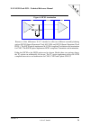
Nat-mch clock-pcb – technical reference manual version 1.4 © n.A.T. Gmbh 20 figure 4: hcsl termination because of this differences n.A.T. Decided to offer two different assembly/ordering options sscm (spread spectrum clock m-lvds) and ssch (spread spectrum clock hcsl). The sscm option implements m-l...
Page 21: 9 Location
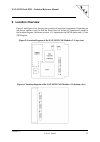
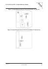
Nat-mch clock-pcb – technical reference manual version 1.4 © n.A.T. Gmbh 21 9 location overview figure 5 and figure 6 areshowing the position of important components. Depending on the chosen options it may be that the board does not include all components named in the location diagram. Hardware revi...
Page 22
Nat-mch clock-pcb – technical reference manual version 1.4 © n.A.T. Gmbh 22 figure 7: location diagram of the nat-mch clk module v2.3 (top-view) figure 8: location diagram of the nat-mch clk module v2.3 (bottom-view).
Page 23: 10 Connectors
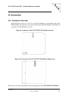
Nat-mch clock-pcb – technical reference manual version 1.4 © n.A.T. Gmbh 23 10 connectors 10.1 connector overview since hardware revision v2.1 and v2.3 of the clk module are compatible to the other mch modules all connectors are at the same position. Therefore figure 9 and figure 10 are guilty for b...
Page 24
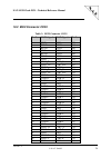
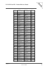
Nat-mch clock-pcb – technical reference manual version 1.4 © n.A.T. Gmbh 24 10.2 mch connector con1 table 3: mch connector con1 pin no. Mch-signal mch-signal pin no. 1 gnd gnd 170 2 rsvd rsvd 169 3 rsvd rsvd 168 4 gnd gnd 167 5 rsvd rsvd 166 6 rsvd rsvd 165 7 gnd gnd 164 8 clk3_tx+ clk3_rx+ 163 9 cl...
Page 25
Nat-mch clock-pcb – technical reference manual version 1.4 © n.A.T. Gmbh 25 pin no. Mch-signal mch-signal pin no. 38 clk3-3+ clk3-9+ 133 39 clk3-3- clk3-9- 132 40 gnd gnd 131 41 clk3-4+ clk3-10+ 130 42 clk3-4- clk3-10- 129 43 gnd gnd 128 44 clk3-5+ clk3-11+ 127 45 clk3-5- clk3-11- 126 46 gnd gnd 125...
Page 26
Nat-mch clock-pcb – technical reference manual version 1.4 © n.A.T. Gmbh 26 pin no. Mch-signal mch-signal pin no. 79 gnd gnd 92 80 clk1-11+ clk2-11+ 91 81 clk1-11- clk2-11- 90 82 gnd gnd 89 83 clk1-12+ clk2-12+ 88 84 clk1-12- clk2-12- 87 85 gnd gnd 86 10.3 connector con2: interface to basic-pcb conn...
Page 27
Nat-mch clock-pcb – technical reference manual version 1.4 © n.A.T. Gmbh 27 10.4 connector con3: interface to hub-pcb connector con3 connects the clk module with the hub-pcb. Table 5: connector to hub-pcb con3 pin no. Signal signal pin no. 1 +12v +12v 2 3 +12v +12v 4 5 pcieclk_p +3.3v mp 6 7 pcieclk...
Page 28: 11.1 Spi Interface
Nat-mch clock-pcb – technical reference manual version 1.4 © n.A.T. Gmbh 28 11 nat-mch clk module programming notes 11.1 spi interface the spi interface on the clk module is used only for maintenance purposes, e.G. Updating the microcontroller firmware. 11.2 i²c interface the i²c interface is the ma...
Page 29
Nat-mch clock-pcb – technical reference manual version 1.4 © n.A.T. Gmbh 29 11.3.1 board identifier register the board identifier register contains the board id that identifies the board as nat-mch clk module. Table 7: board identifier register board identifier - address 0x00 default value 0xb4 bit ...
Page 30
Nat-mch clock-pcb – technical reference manual version 1.4 © n.A.T. Gmbh 30 11.3.4 fpga revision register the fpga revision register contains the revision code of the altera fpga. Table 10: fpga revision register fpga revision - address 0x03 default value # of running fpga revision bit 7 6 5 4 3 2 1...
Page 31
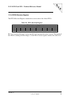
Nat-mch clock-pcb – technical reference manual version 1.4 © n.A.T. Gmbh 31 11.3.5 reference 0 selection register the value of the reference 0 selection register decides which source is connected to ref0 of the pll. Table 11: ref0_sel register reference 0 selection - address 0x04 default value 0x00 ...
Page 32
Nat-mch clock-pcb – technical reference manual version 1.4 © n.A.T. Gmbh 32 11.3.6 reference 1 selection register the value of the reference 1 selection register decides which source is connected to ref1 of the pll. Table 13: ref1_sel register reference 1 selection - address 0x05 default value 0x00 ...
Page 33
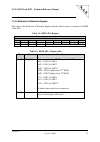
Nat-mch clock-pcb – technical reference manual version 1.4 © n.A.T. Gmbh 33 11.3.7 source selection 1 register the value of the source selection 1 register decides which output (of the pll) is connected to the clk1 transceiver. Table 15: src_sel1 register source selection 1 - address 0x06 default va...
Page 34
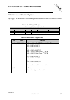
Nat-mch clock-pcb – technical reference manual version 1.4 © n.A.T. Gmbh 34 11.3.8 source selection 2 register the value of the source selection 2 register decides which output (of the pll) is connected to the clk2 transceiver. Table 17: src_sel2 register source selection 2 – address 0x07 default va...
Page 35
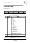
Nat-mch clock-pcb – technical reference manual version 1.4 © n.A.T. Gmbh 35 11.3.9 source selection 3 register the value of the source selection 3 register decides which output (of the pll) is connected to the clk3 transceiver. Table 19: src_sel3 register source selection 3 – address 0x08 default va...
Page 36
Nat-mch clock-pcb – technical reference manual version 1.4 © n.A.T. Gmbh 36 11.3.10 source selection clk1 update register the value of the source selection clk1 update register decides which output (of the pll) is connected to the update clk1 transceiver. Table 21: src_sel_clk1_ud register source se...
Page 37
Nat-mch clock-pcb – technical reference manual version 1.4 © n.A.T. Gmbh 37 11.3.11 source selection clk3 update register the value of the source selection clk3 update register decides which output (of the pll) is connected to the update clk3 transceiver. Table 23: src_sel_clk3_ud register source se...
Page 38
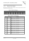
Nat-mch clock-pcb – technical reference manual version 1.4 © n.A.T. Gmbh 38 11.3.12 transceiver control 1 register the value of the transceiver control 1 register controls the receive function of all m-lvds transceiver and the transmit function of the update m-lvds transceiver. Table 25: transc_ctl1...
Page 39
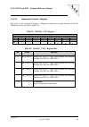
Nat-mch clock-pcb – technical reference manual version 1.4 © n.A.T. Gmbh 39 11.3.13 transceiver control 2 register the value of the transceiver control 2 register controls the transmit function of the m- lvds transceiver for clk1, amc1-8. Table 27: transc_ctl2 register transceiver control 2 - addres...
Page 40
Nat-mch clock-pcb – technical reference manual version 1.4 © n.A.T. Gmbh 40 11.3.14 transceiver control 3 register the value of the transceiver control 3 register controls the transmit function of the m- lvds transceiver for clk1, amc9-12. Table 29: transc_ctl3 register transceiver control 3 - addre...
Page 41
Nat-mch clock-pcb – technical reference manual version 1.4 © n.A.T. Gmbh 41 11.3.15 transceiver control 4 register the value of the transceiver control 4 register controls the transmit function of the m- lvds transceiver for clk2, amc1-8. Table 31: transc_ctl4 register transceiver control 4 - addres...
Page 42
Nat-mch clock-pcb – technical reference manual version 1.4 © n.A.T. Gmbh 42 11.3.16 transceiver control 5 register the value of the transceiver control 5 register controls the transmit function of the m- lvds transceiver for clk2, amc9-12. Table 33: transc_ctl5 register transceiver control 5 - addre...
Page 43
Nat-mch clock-pcb – technical reference manual version 1.4 © n.A.T. Gmbh 43 11.3.17 transceiver control 6 register the value of the transceiver control 6 register controls the transmit function of the m- lvds transceiver for clk3, amc1-8. Table 35: transc_ctl6 register transceiver control 6 - addres...
Page 44
Nat-mch clock-pcb – technical reference manual version 1.4 © n.A.T. Gmbh 44 11.3.18 transceiver control 7 register the value of the transceiver control 7 register controls the transmit function of the m- lvds transceiver for clk3, amc9-12. Table 37: transc_ctl7 register transceiver control 7 - addre...
Page 45
Nat-mch clock-pcb – technical reference manual version 1.4 © n.A.T. Gmbh 45 11.3.19 pll control 1 register the pll control 1 register manages together with the pll_ctr2 register the control inputs of the zarlink pll. Table 39: pll_ctr1 register pll control 1 - address 0x12 default value 0x00 bit 7 6...
Page 46
Nat-mch clock-pcb – technical reference manual version 1.4 © n.A.T. Gmbh 46 11.3.20 pll control 2 register the pll control 2 register manages together with the pll_ctr1 register the control inputs of the zarlink pl l. Table 41: pll_ctr2 register pll control 2 - address 0x13 default value 0x00 bit 7 ...
Page 47
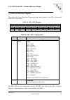
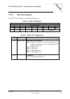
Nat-mch clock-pcb – technical reference manual version 1.4 © n.A.T. Gmbh 47 11.3.21 pll output signals register the pll output signals register shows the state of the pll output signals. Table 43: pll_outp register pll output signals - address 0x14 default value 0x00 bit 7 6 5 4 3 2 1 0 access r r r...
Page 48
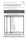
Nat-mch clock-pcb – technical reference manual version 1.4 © n.A.T. Gmbh 48 11.3.22 reserved register the reserved register bytes are used for n.A.T. Internal tests. Do not change the value of these registers. Table 45: res_1 register reserved 1 - address 0x15 default value 0x00 bit 7 6 5 4 3 2 1 0 ...
Page 49
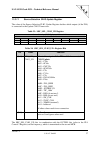
Nat-mch clock-pcb – technical reference manual version 1.4 © n.A.T. Gmbh 49 table 50: res_6 register reserved 6 - address 0x1a default value 0x00 bit 7 6 5 4 3 2 1 0 access r/w r/w r/w r/w r/w r/w r/w r/w func - - - - - - - - 11.3.23 synchronized clock register the synchronized clock register contai...
Page 50
Nat-mch clock-pcb – technical reference manual version 1.4 © n.A.T. Gmbh 50 table 52: sync_clk - register bits bit name function [4..0] sync_clk_ sel the sync clock selection bits control the sync_clk multiplexer. The output of this multiplexer can be selected as a source for the clk1-3. 0x01 – c19o...
Page 51
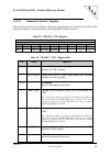
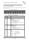
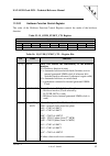
Nat-mch clock-pcb – technical reference manual version 1.4 © n.A.T. Gmbh 51 11.3.24 led2 control register the led2 control register selects the led2 function. Table 53: led2_ctr register led2 control - address 0x1c default value 0x00 bit 7 6 5 4 3 2 1 0 access r r r r r r/w r/w r/w func - - - - - le...
Page 52
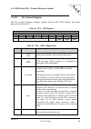
Nat-mch clock-pcb – technical reference manual version 1.4 © n.A.T. Gmbh 52 11.3.25 holdover function control register the value of the holdover function control register controls the mode of the holdover function. Table 55: h_over_funkt_ctl register holdover function control - address 0x2d default ...
Page 53
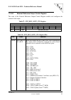
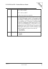
Nat-mch clock-pcb – technical reference manual version 1.4 © n.A.T. Gmbh 53 11.3.26 external reference output control register the value of the external reference output control register enables and configures the external clock outpu. Table 57: ext_ref_outp_ctl register external referenceoutput con...
Page 54
Nat-mch clock-pcb – technical reference manual version 1.4 © n.A.T. Gmbh 54 0x31 – clk1 of amc1 0x32 – clk1 of amc2 : 0x3c – clk1 of amc12 all other values result in no connection 6 high-ampl selects the amplitude of the output signal the clk-module output connects via two signals to the base-module...
Page 55: Known Bugs / Restrictions
Nat-mch clock-pcb – technical reference manual version 1.4 © n.A.T. Gmbh 55 known bugs / restrictions none.
Page 56
Nat-mch clock-pcb – technical reference manual version 1.4 © n.A.T. Gmbh 56 appendix a: reference documentation [1] zarlink, zl30105 t1/e1/sdh stratum 3 redundant system clock synchronizer for advancedtca™ and h.110, 11/05.
Page 57
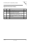
Nat-mch clock-pcb – technical reference manual version 1.4 © n.A.T. Gmbh 57 appendix b: document’s history revision date description author 1.0 12.02.2008 initial revision ks 1.1 13.02.2008 changed sync_clk register description ks 1.2 05.06.2008 12.08.2008 added description of holdover function and ...


