- DL manuals
- National
- Computer Hardware
- CP3BT26
- User manual
National CP3BT26 User manual
©2004 National Semiconductor Corporation
www.national.com
CP3BT26 Connectivity Pr
ocessor with
Bluetooth and Dual CAN Interfaces
PRELIMINARY
MAY 2004
CP3BT26 Reprogrammable Connectivity Processor with
Bluetooth
®
, USB, and CAN Interfaces
1.0
General Description
The CP3BT26 connectivity processor combines high perfor-
mance with the massive integration needed for embedded
Bluetooth applications. A powerful RISC core with on-chip
SRAM and Flash memory provides high computing band-
width, hardware communications peripherals provide high-
I/O bandwidth, and an external bus provides system ex-
pandability.
On-chip communications peripherals include: Bluetooth
Lower Link Controller, Universal Serial Bus (USB) 1.1 node,
CAN, Microwire/Plus, SPI, ACCESS.bus, quad UART, 12-bit
A/D converter, and Advanced Audio Interface (AAI). Addi-
tional on-chip peripherals include Random Number Gener-
ator (RNG), DMA controller, CVSD/PCM conversion
module, Timing and Watchdog Unit, Versatile Timer Unit,
Multi-Function Timer, and Multi-Input Wake-Up (MIWU)
unit.
Bluetooth hand-held devices can be both smaller and lower
in cost for maximum consumer appeal. The low voltage and
advanced power-saving modes achieve new design points
in the trade-off between battery size and operating time for
handheld and portable applications.
In addition to providing the features needed for the next gen-
eration of embedded Bluetooth products, the CP3BT26 is
backed up by the software resources designers need for
rapid time-to-market, including an operating system, Blue-
tooth protocol stack implementation, peripheral drivers, ref-
erence designs, and an integrated development
environment. Combined with a Bluetooth radio transceiver
such as National’s LMX5252, the CP3BT26 provides a com-
plete Bluetooth system solution.
National Semiconductor offers a complete and industry-
proven application development environment for CP3BT26
applications, including the IAR Embedded Workbench,
iSYSTEM winIDEA and iC3000 Active Emulator, Bluetooth
Development Board, Bluetooth Protocol Stack, and Applica-
tion Software.
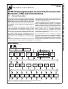
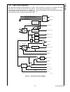
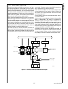
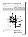
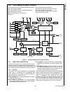
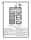
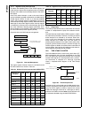
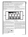
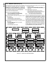
Block Diagram
CPU Core Bus
12 MHz and 32 kHz
Oscillator
Peripheral Bus
PLL and Clock
Generator
Power-on-Reset
Bus
Interface
Unit
Peripheral
Bus
Controller
Serial
Debug
Interface
DMA
Controller
Interrupt
Control
Unit
CVSD/PCM
Converter
Power
Manage-
ment
Timing and
Watchdog
Unit
8-Channel
12-bit ADC
Versatile
Timer Unit
Muti-Func-
tion Timer
Multi-Input
Wake-Up
GPIO
Audio
Interface
Microwiire/
SPI
Quad UART
Clock Generator
Protocol
Core
RF Interface
Bluetooth Lower
Link Controller
4.5K Bytes
Data RAM
1K Byte
Sequencer RAM
DS202
256K Bytes
Flash
Program
Memory
8K Bytes
Flash
Data
32K Bytes
Static
RAM
CR16C
CPU Core
ACCESS
.bus
CAN 2.0B
Controller
Random
Number
Generator
USB
Bluetooth is a registered trademark of Bluetooth SIG, Inc. and is used under license by National Semiconductor.
TRI-STATE is a registered trademark of National Semiconductor Corporation.
Summary of CP3BT26
Page 1
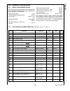
©2004 national semiconductor corporation www.National.Com cp3bt26 connectivity pr ocessor with bluetooth and dual can interfaces preliminary may 2004 cp3bt26 reprogrammable connectivity processor with bluetooth ® , usb, and can interfaces 1.0 general description the cp3bt26 connectivity processor co...
Page 2
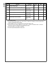
Www.National.Com 2 cp3bt26 table of contents 1.0 general description . . . . . . . . . . . . . . . . . . . . . . . . . . 1 2.0 features . . . . . . . . . . . . . . . . . . . . . . . . . . . . . . . . . . . . 3 3.0 device overview . . . . . . . . . . . . . . . . . . . . . . . . . . . . . 4 3.1 cr16c ...
Page 3
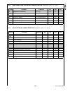
3 www.National.Com cp3 bt26 2.0 features cpu features fully static risc processor core, capable of operating from 0 to 24 mhz with zero wait/hold states minimum 41.7 ns instruction cycle time with a 24-mhz in- ternal clock frequency, based on a 12-mhz external input 47 independently vectored p...
Page 4
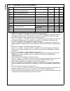
Www.National.Com 4 cp3bt26 3.0 device overview the cp3bt26 connectivity processor is a complete micro- computer with all system timing, interrupt logic, program memory, data memory, and i/o ports included on-chip, mak- ing it well-suited to a wide range of embedded applications. The block diagram on...
Page 5
5 www.National.Com cp3 bt26 3.7 bluetooth llc the integrated hardware bluetooth lower link controller (llc) complies to the bluetooth specification version 1.1 and integrates the following functions: 4.5k-byte dedicated bluetooth data ram 1k-byte dedicated bluetooth sequencer ram support of al...
Page 6
Www.National.Com 6 cp3bt26 3.14 random number generator rng peripheral for use in trusted computer peripheral ap- plications (tcpa) to improve the authenticity, integrity, and privacy of internet-based communication and commerce. 3.15 microwire/spi the microwire/spi (mwspi) interface module supports...
Page 7
7 www.National.Com cp3 bt26 3.21 power management the power management module (pmm) improves the effi- ciency of the device by changing the operating mode and power consumption to match the required level of activity. The device can operate in any of four power modes: — active: the device operates a...
Page 8
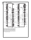
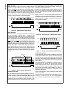
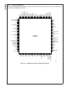
Www.National.Com 8 cp3bt26 4.0 signal descriptions figure 1. Cp3bt26 device signals some pins may be enabled as general-purpose i/o-port pins or as alternate functions associated with specific pe- ripherals or interfaces. These pins may be individually con- figured as port pins, even when the associ...
Page 9
9 www.National.Com cp3 bt26 table 2 cp3bt26 lqfp-128 signal descriptions name pins i/o primary function alternate name alternate function x1cki 1 input 12 mhz oscillator input bbclk bb reference clock for the rf interface x1cko 1 output 12 mhz oscillator output none none x2cki 1 input 32 khz oscilla...
Page 10
Www.National.Com 10 cp3bt26 adc3 1 i/o adc input channel 3 tsy- touchscreen y- contact adc4 1 i/o adc input channel 4 muxout0 analog multiplexer output 0 adc5 1 i/o adc input channel 5 muxout1 analog multiplexer output 1 adc6 1 input adc input channel 6 none none adc7 1 input adc input channel 7 adc...
Page 11
11 www.National.Com cp3 bt26 pg4 1 i/o generic i/o sdat bt serial i/f data pg5 1 i/o generic i/o sle bt serial i/f load enable output pg6 1 i/o generic i/o wui10 multi-input wake-up channel 10 btseq2 bluetooth sequencer status pg7 1 i/o generic i/o ta multi function timer port a btseq3 bluetooth seq...
Page 12
Www.National.Com 12 cp3bt26 table 3 cp3bt26 lqfp-144 signal descriptions name pins i/o primary function alternate name alternate function x1cki 1 input 12 mhz oscillator input bbclk bb reference clock for the rf interface x1cko 1 output 12 mhz oscillator output none none x2cki 1 input 32 khz oscilla...
Page 13
13 www.National.Com cp3 bt26 adc3 1 i/o adc input channel 3 tsy- touchscreen y- contact adc4 1 i/o adc input channel 4 muxout0 analog multiplexer output 0 adc5 1 i/o adc input channel 5 muxout1 analog multiplexer output 1 adc6 1 input adc input channel 6 none none adc7 1 input adc input channel 7 ad...
Page 14
Www.National.Com 14 cp3bt26 pf6 1 i/o generic i/o std aai transmit data output tio7 versatile timer channel 7 pf7 1 i/o generic i/o srd aai receive data input tio8 versatile timer channel 8 pg0 1 i/o generic i/o rfsync bt ac correlation/tx enable output pg1 1 i/o generic i/o rfce bt rf chip enable o...
Page 15
15 www.National.Com cp3 bt26 5.0 cpu architecture the cp3bt26 uses the cr16c third-generation 16-bit compactrisc processor core. The cpu implements a re- duced instruction set computer (risc) architecture that al- lows an effective execution rate of up to one instruction per clock cycle. For a detai...
Page 16
Www.National.Com 16 cp3bt26 5.2.4 interrupt base register (intbase) the intbase register holds the address of the dispatch ta- ble for exceptions. The dispatch table can be located any- where in the cpu address space. When loading the intbase register, bits 31 to 24 and bit 0 must written with 0. 5....
Page 17
17 www.National.Com cp3 bt26 5.4 configuration register (cfg) the cfg register is used to enable or disable various oper- ating modes and to control optional on-chip caches. Be- cause the cp3bt26 does not have cache memory, the cache control bits in the cfg register are reserved. All cfg bits are cl...
Page 18
Www.National.Com 18 cp3bt26 5.5 addressing modes the cr16c cpu core implements a load/store architec- ture, in which arithmetic and logical instructions operate on register operands. Memory operands are made accessible in registers using load and store instructions. For efficient implementation of i...
Page 19
19 www.National.Com cp3 bt26 5.6 stacks a stack is a last-in, first-out data structure for dynamic stor- age of data and addresses. A stack consists of a block of memory used to hold the data and a pointer to the top of the stack. As more data is pushed onto a stack, the stack grows downward in memo...
Page 20
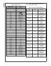
Www.National.Com 20 cp3bt26 table 5 instruction set summary mnemonic operands description movi rsrc/imm, rdest move movxb rsrc, rdest move with sign extension movzb rsrc, rdest move with zero extension movxw rsrc, rpdest move with sign extension movzw rsrc, rpdest move with zero extension movd imm, ...
Page 21
21 www.National.Com cp3 bt26 ashud rsrc/imm, rpdest arithmetic left/right shift lshi rsrc/imm, rdest logical left/right shift lshd rsrc/imm, rpdest logical left/right shift sbiti iposition, disp(rbase) set a bit in memory (because this instruction treats the destination as a read- modify-write opera...
Page 22
Www.National.Com 22 cp3bt26 retx return from exception push imm, rsrc, ra push “imm” number of registers on user stack, starting with rsrc and possibly including ra pop imm, rdest, ra restore “imm” number of registers from user stack, starting with rdest and possibly including ra popret imm, rdest, ...
Page 23
23 www.National.Com cp3 bt26 stormp imm3 store 1 to 8 registers (r2-r5, r8-r11) to memory starting at (r7,r6) di disable maskable interrupts ei enable maskable interrupts eiwait enable maskable interrupts and wait for interrupt nop no operation wait wait for interrupt table 5 instruction set summary...
Page 24
Www.National.Com 24 cp3bt26 6.0 memory the cp3bt26 supports a uniform 16m-byte linear address space. Table 6 lists the types of memory and peripherals that occupy this memory space. Unlisted address ranges are reserved and must not be read or written. The biu zones are regions of the address space t...
Page 25
25 www.National.Com cp3 bt26 6.2 bus interface unit (biu) the biu controls the interface between the cpu core bus and those on-chip modules which are mapped into biu zones. These on-chip modules are the flash program mem- ory and the i/o zone. The biu controls the configured pa- rameters for bus acc...
Page 26
Www.National.Com 26 cp3bt26 6.4.2 i/o zone configuration register (iocfg) the iocfg register is a word-wide, read/write register that controls the timing and bus characteristics of accesses to the 256-byte i/o zone memory space (ff fb00h to ff fbffh). The registers associated with port b and port c ...
Page 27
27 www.National.Com cp3 bt26 ipre the preliminary idle bit controls whether an idle cycle is inserted prior to the current bus cycle, when the new bus cycle accesses a dif- ferent zone. No idle cycles are required for on- chip accesses. 0 – no idle cycle (recommended). 1 – idle cycle inserted. 6.4.4...
Page 28
Www.National.Com 28 cp3bt26 fre the fast read enable bit controls whether fast read bus cycles are used. A fast read op- eration takes one clock cycle. A normal read operation takes at least two clock cycles. 0 – normal read cycles. 1 – fast read cycles. Ipst the post idle bit controls whether an id...
Page 29
29 www.National.Com cp3 bt26 7.0 system configuration registers the system configuration registers control and provide sta- tus for certain aspects of device setup and operation, such as indicating the states sampled from the env[2:0] inputs. The system configuration registers are listed in table 9....
Page 30
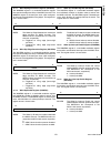
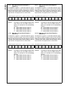
Www.National.Com 30 cp3bt26 7.2 module status register (mstat) the mstat register is a byte-wide, read-only register that indicates the general status of the device. The mcfg regis- ter format is shown below. Oenv2:0 the operating environment bits hold the states sampled from the env[2:0] input pins...
Page 31
31 www.National.Com cp3 bt26 8.0 flash memory the flash memory consists of the flash program memory and the flash data memory. The flash program memory is further divided into the boot area and the code area. A special protection scheme is applied to the lower portion of the flash program memory, ca...
Page 32
Www.National.Com 32 cp3bt26 8.2.1 main block 0 and 1 main block 0 and main block 1 hold the 256k-byte program space, which consists of the boot area and code area. Each block consists of sixteen 8k-byte sections. Write ac- cess by the cpu to main block 0 and main block 1 is con- trolled by the corre...
Page 33
33 www.National.Com cp3 bt26 8.3.3 main block page erase a flash erase operation sets all of the bits in the erased re- gion. Pages of a main block can be individually erased if their write enable bits are set. This method cannot be used to erase the boot area, if defined. Each page in main block 0 ...
Page 34
Www.National.Com 34 cp3bt26 8.4 information block words two words in the information blocks are dedicated to hold settings that affect the operation of the system: the function word in information block 0 and the protection word in in- formation block 1. 8.4.1 function word the function word resides...
Page 35
35 www.National.Com cp3 bt26 rdprot the rdprot field controls the global read protection mechanism for the on-chip flash program memory. If a majority of the three rdprot bits are clear, the flash program memory is protected against read access from the serial debug interface or an external flash pr...
Page 36
Www.National.Com 36 cp3bt26 8.5.1 flash memory information block address register (fmibar/fsmibar) the fmibar register specifies the 8-bit address for read or write access to an information block. Because only word ac- cess to the information blocks is supported, the least signif- icant bit (lsb) of...
Page 37
37 www.National.Com cp3 bt26 8.5.5 flash data memory 0 write enable register (fsm0wer) the fsm0wer register controls write protection for the flash data memory. The data block is divided into 16 512- byte sections. Each bit in the fsm0wer register controls write protection for one of these sections....
Page 38
Www.National.Com 38 cp3bt26 8.5.7 flash memory status register (fmstat/ fsmstat) this register reports the currents status of the on-chip flash memory. The flsr register is clear after device reset. The cpu bus master has read/write access to this register. Eerr the erase error bit indicates whether...
Page 39
39 www.National.Com cp3 bt26 8.5.10 flash memory transition time reload register (fmtran/fsmtran) the fmtran/fmstran register is a byte-wide read/write register that controls some program/erase transition times. Software must not modify this register while program/erase operation is in progress (fmb...
Page 40
Www.National.Com 40 cp3bt26 8.5.16 flash memory recovery time reload register (fmrcv/fsmrcv) the fmrcv/fsmrcv register is a byte-wide read/write register that controls the recovery delay time between two flash memory accesses. Software must not modify this reg- ister while a program/erase operation ...
Page 41
41 www.National.Com cp3 bt26 9.0 dma controller the dma controller (dmac) has a register-based program- ming interface, as opposed to an interface based on i/o control blocks. After loading the registers with source and destination addresses, as well as block size and type of op- eration, a dmac cha...
Page 42
Www.National.Com 42 cp3bt26 direct mode supports two bus policies: intermittent and con- tinuous. In intermittent mode, the dmac gives bus master- ship back to the cpu after every cycle. In continuous mode, the dmac remains bus master until the transfer is complet- ed. The maximum bus throughput in ...
Page 43
43 www.National.Com cp3 bt26 if the dmastat.Vld bit is clear: 1. The transfer operation terminates. 2. The channel sets the dmastat.Ovr bit. 3. The dmastat.Chac bit is cleared. 4. An interrupt is generated if enabled by the dmacntln.Eovr bit. The dmacntln.Chen bit must be cleared before loading the ...
Page 44
Www.National.Com 44 cp3bt26 9.6.1 device a address counter register (adcan) the device a address counter register is a 32-bit, read/ write register. It holds the current 24-bit address of either the source data item or the destination location, depending on the state of the dir bit in the cntln regi...
Page 45
45 www.National.Com cp3 bt26 9.6.6 block length register (bltrn) the block length register is a 16-bit, read/write register. It holds the number of dma transfers to be performed for the next block. Writing this register automatically sets the dm- astat.Vld bit. Note: 0000h is interpreted as 2 16 -1 ...
Page 46
Www.National.Com 46 cp3bt26 9.6.8 dma status register (dmastat) the dma status register is a byte-wide, read register that holds the status information for the dma channel n. This register is cleared at reset. The reserved bits always return zero when read. The vld, ovr and tc bits are sticky (once ...
Page 47
47 www.National.Com cp3 bt26 10.0 interrupts the interrupt control unit (icu) receives interrupt requests from internal and external sources and generates interrupts to the cpu. Interrupts from the timers, uarts, microwire/ spi interface, and multi-input wake-up module are all maskable interrupts. T...
Page 48
Www.National.Com 48 cp3bt26 10.3.1 interrupt vector register (ivct) the ivct register is a byte-wide read-only register which re- ports the encoded value of the highest priority maskable in- terrupt that is both asserted and enabled. The valid range is from 10h to 3fh. The register is read by the cp...
Page 49
49 www.National.Com cp3 bt26 10.3.4 interrupt enable and mask register 0 (ienam0) the ienam0 register is a word-wide read/write register which holds bits that individually enable and disable the maskable interrupt sources irq1 through irq15. The reg- ister is initialized to ffffh at reset. Iena each...
Page 50
Www.National.Com 50 cp3bt26 10.4 maskable interrupt sources table 20 shows the interrupts assigned to various on-chip maskable interrupts. The priority of simultaneous maskable interrupts is linear, with irq47 having the highest priority. Table 20 maskable interrupts assignment all reserved interrup...
Page 51
51 www.National.Com cp3 bt26 11.0 triple clock and reset the triple clock and reset module generates a 12 mhz main clock and a 32.768 khz slow clock from external crystal networks or external clock sources. It provides vari- ous clock signals for the rest of the chip. It also provides the main syste...
Page 52
Www.National.Com 52 cp3bt26 11.1 external crystal network an external crystal network is connected to the x1cki and x1cko pins to generate the main clock, unless an external clock signal is driven on the x1cki pin. A similar external crystal network may be used at pins x2cki and x2cko for the slow c...
Page 53
53 www.National.Com cp3 bt26 choose capacitor component values in the tables to obtain the specified load capacitance for the crystal when com- bined with the parasitic capacitance of the trace, socket, and package (which can vary from 0 to 8 pf). As a guideline, the load capacitance is: c2 > c1 c1 ...
Page 54
Www.National.Com 54 cp3bt26 11.5 system clock the system clock drives most of the on-chip modules, in- cluding the cpu. Typically, it is driven by the main clock, but it can also be driven by the pll. In either case, the clock sig- nal is passed through a programmable divider (scale factors from ÷1 ...
Page 55
55 www.National.Com cp3 bt26 fclk bit cannot be cleared until the pll clock has stabilized. After reset this bit is set. 0 – pll is active. 1 – pll is powered down. Ace1 when the auxiliary clock enable bit is set and a stable main clock is provided, the auxiliary clock 1 prescaler is enabled and gen...
Page 56
Www.National.Com 56 cp3bt26 12.0 power management the power management module (pmm) improves the effi- ciency of the cp3bt26 by changing the operating mode (and therefore the power consumption) according to the re- quired level of device activity. The device implements four power modes: active p...
Page 57
57 www.National.Com cp3 bt26 12.3 idle mode in idle mode, the system clock is disabled and therefore the clock is stopped to most modules of the device. The pll and the high-frequency oscillator may be disabled as con- trolled by register bits. The low-frequency oscillator remains active. The power ...
Page 58
Www.National.Com 58 cp3bt26 halt the halt mode bit indicates whether the de- vice is in halt mode. Before entering halt mode, the wbpsm bit must be set. When the halt bit is written with 1, the device enters the halt mode at the execution of the next wait instruction. When in halt mode, the pmm stop...
Page 59
59 www.National.Com cp3 bt26 12.6.2 power management status register (pmmsr) the management status register (pmmr) is a byte-wide, read/write register that provides status signals for the vari- ous clocks. The reset value of pmsr register bits 0 to 2 de- pend on the status of the clock sources monit...
Page 60
Www.National.Com 60 cp3bt26 12.7.2 entering idle mode entry into idle mode is performed by writing a 1 to the pm- mcr.Idle bit and then executing a wait instruction. The pmmcr.Wbpsm bit must be set before the wait instruc- tion is executed. Idle mode can be entered only from the ac- tive or power sa...
Page 61
61 www.National.Com cp3 bt26 13.0 multi-input wake-up the multi-input wake-up (miwu) unit consists of two iden- tical 16-channel modules. Each module can assert a wake- up signal for exiting from a low-power mode, and each can assert an interrupt request on any of four interrupt control unit (icu) c...
Page 62
Www.National.Com 62 cp3bt26 13.1 multi-input wake-up registers table 28 lists the miwu registers. Table 27 miwu sources miwu channel source wui0 twm t0out wui1 access.Bus wui2 canrx wui3 mwcs wui4 uart0 cts wui5 uart0 rxd wui6 bluetooth llc wui7 aai sfs wui8 usb wake-up wui9 pj7 wui10 pg6 wui11 ph0 ...
Page 63
63 www.National.Com cp3 bt26 13.1.1 wake-up edge detection register (wk0edg) the wk0edg register is a word-wide read/write register that controls the edge sensitivity of the miwu channels. The wk0edg register is cleared upon reset, which configures all channels to be triggered on rising edges. The r...
Page 64
Www.National.Com 64 cp3bt26 13.1.7 wake-up interrupt control register 1 (wk0ictl1) the wk0ictl1 register is a word-wide read/write register that selects the interrupt request signal for the associated miwu channels wui7:0. At reset, the wk0ictl1 register is cleared, which selects miwu interrupt requ...
Page 65
65 www.National.Com cp3 bt26 13.1.11 wake-up pending register (wk0pnd) the wk0pnd register is a word-wide read/write register in which the multi-input wake-up module latches any detect- ed trigger conditions. The cpu can only write a 1 to any bit position in this register. If the cpu attempts to wri...
Page 66
Www.National.Com 66 cp3bt26 13.2 programming procedures to set up and use the multi-input wake-up function, use the following procedure. Performing the steps in the order shown will prevent false triggering of a wake-up condition. This same procedure should be used following a reset be- cause the wa...
Page 67
67 www.National.Com cp3 bt26 14.0 input/output ports each device has up to 54 software-configurable i/o pins, or- ganized into 8-bit ports (not all bits are used in some ports). The ports are named port b, port c, port e, port f, port g, port h, and port j. In addition to their general-purpose i/o c...
Page 68
Www.National.Com 68 cp3bt26 in the descriptions of the ports and port registers, the lower- case letter “x” represents the port designation, either b, c, e, f, g, h, or j. For example, “pxdir register” means any one of the port direction registers: pbdir, pcdir, pedir, pfdir, pgdir, phdir, or pjdir....
Page 69
69 www.National.Com cp3 bt26 all of the port registers are byte-wide read/write registers, except for the port data input registers, which are read-only registers. Each register bit controls the function of the cor- responding port pin. For example, pgdir.2 (bit 2 of the pgdir register) controls the...
Page 70
Www.National.Com 70 cp3bt26 14.1.6 port high drive strength register (pxhdrv) the pxhdrv register is a byte-wide, read/write register that controls the slew rate of the corresponding pins. The high drive strength function is enabled when the corresponding bits of the pxhdrv register are set. In both...
Page 71
71 www.National.Com cp3 bt26 14.2 open-drain operation a port pin can be configured to operate as an inverting open-drain output buffer. To do this, the cpu must clear the bit in the data output register (pxdout) and then use the port direction register (pxdir) to set the value of the port pin. With...
Page 72
Www.National.Com 72 cp3bt26 15.0 bluetooth controller the integrated hardware bluetooth lower link controller (llc) complies to the bluetooth specification version 1.1 and integrates the following functions: 4.5k-byte dedicated bluetooth data ram 1k-byte dedicated bluetooth sequencer ram suppo...
Page 73
73 www.National.Com cp3 bt26 transmitter circuit of the radio chip is enabled, correspond- ing to the settings of the power control register in the radio chip. The rfsync signal is the alternate function of the general- purpose i/o pin pg0. At reset, this pin is in tri-state mode. Software must enab...
Page 74
Www.National.Com 74 cp3bt26 write operation when the r/w bit is clear, the 16 bits of the data field are shifted out of the cp3bt26 on the falling edge of sclk. Data is sampled by the radio chip on the rising edge of sclk. When sle is high, the 16-bit data are copied into the radio chip register on ...
Page 75
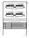
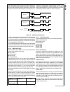
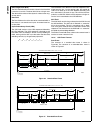
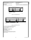
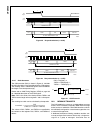
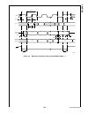
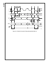
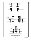
75 www.National.Com cp3 bt26 figure 18. 32-bit write timing figure 19. 32-bit read timing an example of a 32-bit write is shown in table 31. In this ex- ample, the 32-bit value ffff dc04h is written to register address 0ah. In cycle 1, the high word (ffffh) is written. In the first part of cycle 2, ...
Page 76
Www.National.Com 76 cp3bt26 15.3 lmx5251 power-up sequence to power-up a bluetooth system based on the cp3bt26 and lmx5251 devices, the following sequence must be per- formed: 1. Apply vdd to the lmx5251. 2. Apply iovcc and vcc to the cp3bt26. 3. Drive the reset# pin of the lmx5251 high a minimum of...
Page 77
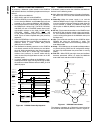
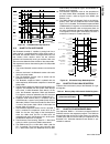
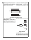
77 www.National.Com cp3 bt26 figure 22. Lmx5252 power-up sequence 15.5 bluetooth sleep mode the bluetooth controller is capable of putting itself into a sleep mode for a specified number of slow clock cycles. In this mode, the controller clocks are stopped internally. The only circuitry which remain...
Page 78
Www.National.Com 78 cp3bt26 15.8 bluetooth shared data ram the shared data ram is a 4.5k memory-mapped section of ram that contains the link control data, rf programming look-up table, and the link payload. This ram can be read and written in the same way as the static ram space and can also be read...
Page 79
79 www.National.Com cp3 bt26 16.0 12-bit analog to digital converter the integrated 12-bit adc provides the following features: 8-input analog multiplexer 8 single-ended channels or 4 differential channels external filtering capability 12-bit resolution with 11-bit accuracy sign bit 15-m...
Page 80
Www.National.Com 80 cp3bt26 the output of the input multiplexer is available externally as the muxout0 and muxout1 signals. In single-ended mode, only muxout0 is used. In differential mode, muxout0 is the positive side and muxout1 is the nega- tive side. The muxout0 and muxout1 outputs and the adcin...
Page 81
81 www.National.Com cp3 bt26 16.2 touchscreen interface the adc provides an interface for 4-wire resistive touch- screens with the resolution necessary for applications such as signature analysis. A typical touchscreen configuration is shown in figure 25. Figure 25. Touchscreen interface a touchscre...
Page 82
Www.National.Com 82 cp3bt26 16.2.2 measuring pen force figure 27 shows equivalent circuits for the driver modes used to measure the x, y, and z coordinates, in which z rep- resents pen force. In this discussion, the ohmic resistance of the drivers is neglected (see section 16.2.3), and series resist...
Page 83
83 www.National.Com cp3 bt26 3. By extension, the adc negative voltage reference can be internally connected to the tsy- terminal, to recover the full 4096 values. The global configuration register (adcgcr) provides the flexibility to implement any of these techniques. 16.3 adc operation in power-sa...
Page 84
Www.National.Com 84 cp3bt26 16.5.1 adc global configuration register (adcgcr) the adcgcr register controls the basic operation of the in- terface. The cpu bus master has read/write access to the adcgcr register. After reset this register is set to 0000h. Clken the clock enable bit controls whether t...
Page 85
85 www.National.Com cp3 bt26 pref_cfg the positive voltage reference configuration field specifies the source of the adc positive voltage reference, according to the following table: nref_cfg the negative voltage reference configura- tion field specifies the source of the adc neg- ative voltage refe...
Page 86
Www.National.Com 86 cp3bt26 16.5.3 adc conversion control register (adccntrl) the adccntrl register specifies the trigger conditions for an adc conversion. Pol the async polarity bit specifies the polarity of edges which trigger adc conversions. 0 – async input is sensitive to rising edges. 1 – asyn...
Page 87
87 www.National.Com cp3 bt26 16.5.6 adc result register (adcreslt) the adcreslt register includes the software-visible end of a 4-word fifo. Conversion results are loaded into the fifo from the 12-bit adc and unloaded when software reads the adcreslt register. The adcreslt register is read-only. Wit...
Page 88
Www.National.Com 88 cp3bt26 17.0 random number generator (rng) the rng unit is a hardware “true random” number genera- tor. When enabled, this unit provides up to 800 random bits per second. The bits are available for reading from a 16-bit register. The rng unit includes two oscillators which operat...
Page 89
89 www.National.Com cp3 bt26 17.2 random number generator register set table 34 lists the rng registers. 17.2.1 rng control and status register (rngcst) the rngcst register provides control and status bits for the rng module. This register is cleared at reset. Rnge the random number generator enable...
Page 90
Www.National.Com 90 cp3bt26 18.0 usb controller the cr16 usb node is an integrated usb node controller that features enhanced dma support with many automatic data handling features. It is compatible with usb specifica- tion versions 1.0 and 1.1. It integrates the required usb transceiver, a serial i...
Page 91
91 www.National.Com cp3 bt26 18.2 endpoint operation 18.2.1 address detection packets are broadcast from the host controller to all nodes on the usb network. Address detection is implemented in hardware to allow selective reception of packets and to per- mit optimal use of cpu bandwidth. One functio...
Page 92
Www.National.Com 92 cp3bt26 bidirectional control endpoint fifo0 operation fifo0 should be used for the bidirectional control endpoint 0. It can be configured to receive data sent to the default ad- dress with the def bit in the epc0 register. Isochronous transfers are not supported for the control ...
Page 93
93 www.National.Com cp3 bt26 receive endpoint fifo operation (rxfifo1, rxfifo2, rxfifo3) the receive fifos for endpoints 2, 4, and 6 support bulk, interrupt, and isochronous usb packet transfers larger than the actual fifo size. If the packet length exceeds the fifo size, software must read the fifo...
Page 94
Www.National.Com 94 cp3bt26 18.3.1 main control register (mcntrl) the mcntrl register controls the main functions of the cr16 usb node. The mcntrl register provides read/write access from the cpu bus. Reserved bits must be written with 0, and they return 0 when read. It is clear after reset. Usben t...
Page 95
95 www.National.Com cp3 bt26 nat the node attached indicates that this node is ready to be detected as attached to usb. When clear, the transceiver forces se0 on the usb node controller to prevent the hub (to which this node is connected) from detecting an attach event. After reset or when the usb n...
Page 96
Www.National.Com 96 cp3bt26 18.3.3 main event register (maev) the main event register summarizes and reports the main events of the usb transactions. This register provides read- only access. The maev register is clear after reset. Warn the warning event bit indicates whether one of the unmasked bit...
Page 97
97 www.National.Com cp3 bt26 sd3 the suspend detect 3 ms bit is set after 3 ms of idle have been detected on the upstream port, indicating that the device should be sus- pended. The suspend occurs under software control by writing the suspend value to the node functional state (nfsr) register. This ...
Page 98
Www.National.Com 98 cp3bt26 18.3.9 receive event register (rxev) the rxev register reports the current status of the fifo, used by the three receive endpoints. The rxev register is clear after reset. It provides read-only access from the cpu bus. Rxfifo the receive fifo n are set whenever either rx_...
Page 99
99 www.National.Com cp3 bt26 18.3.13 fifo warning event register (fwev) the fwev register signals whether a receive or transmit fifo has reached its warning limit. It reports the status for all fifos, except for the endpoint 0 fifo, as no warning limit can be specified for this fifo. The fwev regist...
Page 100
Www.National.Com 100 cp3bt26 mf the missed sof bit is set when the frame number in a valid received sof does not match the expected next value, or when an sof is not received within 12060 bit times. The mf bit provides read-only access. On re- set, this bit is set. This bit is set by the hard- ware ...
Page 101
101 www.National.Com cp3 bt26 dtgl the dma toggle bit is used to determine the initial state of automatic dma (adma) opera- tions. Software initially sets this bit if starting with a data1 operation, and clears this bit if starting with a data0 operation. Writes to this bit also update the ntgl bit ...
Page 102
Www.National.Com 102 cp3bt26 18.3.20 dma mask register (dmamsk) any set bit in the dmamsk register enables automatic set- ting of the dma bit in the altev register when the respec- tive event in the dmaev register occurs. Otherwise, setting the dma bit is disabled. For a description of bits 0 to 3, ...
Page 103
103 www.National.Com cp3 bt26 receive the next packet. The erroneous packet is ignored and not transferred via dma. If this bit is cleared, automatic error handling ceases. 18.3.24 endpoint control 0 register (epc0) the epc0 register controls the mandatory endpoint 0. It is clear after reset. Reserv...
Page 104
Www.National.Com 104 cp3bt26 flush writing a 1 to the flush fifo bit flushes all data from the control endpoint fifos, resets the endpoint to idle state, clears the fifo read and write pointer, and then clears itself. If the endpoint is currently using the fifo0 to transfer data on usb, flushing is ...
Page 105
105 www.National.Com cp3 bt26 flush writing 1 to the flush bit flushes all data from the control endpoint fifos, resets the end- point to idle state, clears the fifo read and write pointer, and then clears itself. If the end- point is currently using fifo0 to transfer data on usb, flushing is delaye...
Page 106
Www.National.Com 106 cp3bt26 ack_stat the acknowledge status bit is valid when the tx_done bit is set. The meaning of the ack_stat bit differs depending on whether iso or non-iso operation is used (as selected by the iso bit in the epcn register). non-isochronous mode — this bit indi- cates the ac...
Page 107
107 www.National.Com cp3 bt26 tfwl the transmit fifo warning limit bits specify how many more bytes can be transmitted from the respective fifo before an underrun con- dition occurs. If the number of bytes remaining in the fifo is equal to or less than the select- ed warning limit, the txwarn bit in...
Page 108
Www.National.Com 108 cp3bt26 18.3.36 receive command register n (rxcn) each of the receive endpoints (2, 4, and 6) has one rxcn register. The registers provide read/write access from the cpu bus. Reading reserved bits returns undefined data. Af- ter reset, it is clear. Rx_en the receive enable bit e...
Page 109
109 www.National.Com cp3 bt26 19.0 can module the can module contains a full can class, can (control- ler area network) serial bus interface for low/high speed ap- plications. It supports reception and transmission of extended frames with a 29-bit identifier, standard frames with an 11-bit identifie...
Page 110
Www.National.Com 110 cp3bt26 figure 34. Can block diagram 19.2 basic can concepts this section provides a generic overview of the basic con- cepts of the controller area network (can). The can protocol is a message-based protocol that allows a total of 2032 (2 11 - 16) different messages in the stan...
Page 111
111 www.National.Com cp3 bt26 the can protocol allows several transmitting modules to start a transmission at the same time as soon as they detect the bus is idle. During the start of transmission, every node monitors the bus line to detect whether its message is over- written by a message with a hi...
Page 112
Www.National.Com 112 cp3bt26 data length code (dlc) the dlc field indicates the number of bytes in the data field. It consists of four bits. The data field can be of length zero. The admissible number of data bytes for a data frame rang- es from 0 to 8. Data field the data field consists of the data...
Page 113
113 www.National.Com cp3 bt26 a can data frame consists of the following fields: start of frame (sof) arbitration field + extended arbitration control field data field cyclic redundancy check field (crc) acknowledgment field (ack) end of frame (eof) remote frame figure 38 shows the str...
Page 114
Www.National.Com 114 cp3bt26 error frame as shown in figure 40, the error frame consists of the error flag and the error delimiter bit fields. The error flag field is built up from the various error flags of the different nodes. Therefore, its length may vary from a minimum of six bits up to a maxim...
Page 115
115 www.National.Com cp3 bt26 figure 42. Interframe space 19.2.4 error types bit error a can device which is currently transmitting also monitors the bus. If the monitored bit value is different from the trans- mitted bit value, a bit error is detected. However, the recep- tion of a “dominant” bit i...
Page 116
Www.National.Com 116 cp3bt26 error active an error active unit can participate in bus communication and may send an active (“dominant”) error flag. Error warning the error warning state is a sub-state of error active to in- dicate a heavily disturbed bus. The can module behaves as in error active mo...
Page 117
117 www.National.Com cp3 bt26 19.2.6 bit time logic in the bit time logic (btl), the can bus speed and the synchronization jump width can be configured by software. The can module divides a nominal bit time into three time segments: synchronization segment, time segment 1 (tseg1), and time segment 2...
Page 118
Www.National.Com 118 cp3bt26 figure 45. Resynchronization (e > sjw) figure 46. Resynchronization (e 19.2.7 clock generator the can prescaler (psc) is shown is figure 47. It divides the cki input clock by the value defined in the ctim register. The resulting clock is called time quanta clock and defi...
Page 119
119 www.National.Com cp3 bt26 independent filtering procedure, which provides the possi- bility to establish a basic-can path. For reception of data frame or remote frames, the can module follows a “receive on first match” rule which means that a given message is only received by one buffer: the fir...
Page 120
Www.National.Com 120 cp3bt26 buffer status field. With this lock function, software has the capability to save several messages with the same identifier or same identifier group into more than one buffer. For ex- ample, a buffer with the second highest priority will receive a message if the buffer w...
Page 121
121 www.National.Com cp3 bt26 all contents of the hidden receive buffer are always copied into the respective receive buffer. This includes the received message id as well as the received data length code (dlc); therefore when some mask bits are set to don’t care, the id field will get the received ...
Page 122
Www.National.Com 122 cp3bt26 figure 54. Buffer read routine (bufflock disabled) the first step is only applicable if polling is used to get the status of the receive buffer. It can be deleted for an interrupt driven receive routine. 1. Read the status (cnstat) of the receive buffer. If the status is...
Page 123
123 www.National.Com cp3 bt26 cnstat status section will be 0101b, as the buffer was rx_full (0100b) before. After finally reading the last re- ceived message, the cpu can reset the buffer to rx_ready. 19.6 transmit structure to transmit a can message, software must configure the message buffer by c...
Page 124
Www.National.Com 124 cp3bt26 ity is combined by the 4-bit txpri value and the 4-bit buffer number (0...14) as shown below. The lowest resulting num- ber results in the highest transmit priority. Table 47 shows the transmit priority configuration if the pri- ority is txpri = 0 for all transmit buffer...
Page 125
125 www.National.Com cp3 bt26 19.6.4 tx buffer states the transmission process can be started after software has loaded the buffer registers (data, id, dlc, pri) and set the buffer status from tx_not_active to tx_once, tx_rtr, or tx_once_rtr. When the cpu writes tx_once, the buffer will be tx_busy a...
Page 126
Www.National.Com 126 cp3bt26 19.7.1 highest priority interrupt code to reduce the decoding time for the cipnd register, the buffer interrupt request with the highest priority is placed as interrupt status code into the ist[3:0] section of the cstp- nd register. Each of the buffer interrupts as well ...
Page 127
127 www.National.Com cp3 bt26 19.9 memory organization the can module occupies 144 words in the memory ad- dress space. This space is organized as 15 banks of 8 words per bank (plus one reserved bank) for the message buffers and 14 words (plus 2 reserved words) for control and status. 19.9.1 cpu acc...
Page 128
Www.National.Com 128 cp3bt26 19.10 can controller registers table 51 lists the can module registers. 19.10.1 buffer status/control register (cnstat) the buffer status (st), the buffer priority (pri), and the data length code (dlc) are controlled by manipulating the con- tents of the buffer status/co...
Page 129
129 www.National.Com cp3 bt26 table 52 buffer status section of the cnstat register st3 (dir) st2 st1 st0 (busy) buffer status 0 0 0 0 rx_not_active 0 0 0 1 reserved for rx_busy. (this condition indicates that soft- ware wrote rx_not_active to a buffer when the data copy process is still active.) 0 ...
Page 130
Www.National.Com 130 cp3bt26 pri the transmit priority code field holds the software-defined transmit priority code for the message buffer. Dlc the data length code field determines the number of data bytes within a received/trans- mitted frame. For transmission, these bits need to be set according ...
Page 131
131 www.National.Com cp3 bt26 19.10.3 storage of messages with less than 8 data bytes the data bytes that are not used for data transfer are “don’t cares”. If the object is transmitted, the data within these bytes will be ignored. If the object is received, the data with- in these bytes will be over...
Page 132
Www.National.Com 132 cp3bt26 19.10.5 storage of remote messages during remote frame transfer, the buffer registers data0– data3 are “don’t cares”. If a remote frame is transmitted, the contents of these registers are ignored. If a remote frame is received, the contents of these registers will be ove...
Page 133
133 www.National.Com cp3 bt26 19.10.6 can global configuration register (cgcr) the can global configuration register (cgcr) is a 16-bit wide register used to: enable/disable the can module. configure the bufflock function for the message buff- er 0..14. enable/disable the time stamp synchroniz...
Page 134
Www.National.Com 134 cp3bt26 figure 61. Data direction bit clear setting the ddir bit will cause the direction of the data stor- age to be reversed — the last byte received is stored at the highest address and the first byte is stored at the lowest ad- dress, as shown in figure 62. Figure 62. Data d...
Page 135
135 www.National.Com cp3 bt26 internal if the internal function is enabled, the cantx and canrx pins of the can module are inter- nally connected to each other. This feature can be used in conjunction with the loop- back mode. This means that the can mod- ule can receive its own sent messages withou...
Page 136
Www.National.Com 136 cp3bt26 tseg1 the time segment 1 field configures the length of the time segment 1 (tseg1). It is not recommended to configure the time seg- ment 1 to be smaller than 2 time quanta. (see table 59). Tseg2 the time segment 2 field specifies the num- ber of time quanta (tq) for pha...
Page 137
137 www.National.Com cp3 bt26 19.10.9 basic mask register (bmskb/bmskx) the bmskb and bmskx registers allow masking the buffer 14, or “don’t care” the incoming extended/standard identifier bits, rtr/xrtr, and ide. Throughout this document, the two 16-bit registers bmskb and bmskx are referenced to a...
Page 138
Www.National.Com 138 cp3bt26 19.10.12 can interrupt clear register (ciclr) the ciclr register bits individually clear can interrupt pending flags caused by the message buffers and from the error management logic. Do not modify this register with in- structions that access the register as a read-modi...
Page 139
139 www.National.Com cp3 bt26 19.10.15 can error counter register (canec) the canec register reports the values of the can receive error counter and the can transmit error counter. Rec the can receive error counter field reports the value of the receive error counter. Tec the can transmit error coun...
Page 140
Www.National.Com 140 cp3bt26 drive the drive bit shows the output value on the cantx pin at the time of the error. Note that a receiver will not drive the bus except during ack and during an active error flag. 19.10.17 can timer register (ctmr) the ctmr register reports the current value of the time...
Page 141
141 www.National.Com cp3 bt26 the critical path derives from receiving a remote frame, which triggers the transmission of one or more data frames. There are a minimum of four bit times in-between two con- secutive frames. These bit times start at the validation point of received frame (reception of ...
Page 142
Www.National.Com 142 cp3bt26 19.12 usage hint under certain conditions, the can module receives a frame sent by itself, even though the loopback feature is disabled. Two conditions must be true to cause this malfunction: a transmit buffer and at least one receive buffer are con- figured with the s...
Page 143
143 www.National.Com cp3 bt26 20.0 advanced audio interface the advanced audio interface (aai) provides a serial syn- chronous, full duplex interface to codecs and similar serial devices. The transmit and receive paths may operate asyn- chronously with respect to each other. Each path uses a 3- wire...
Page 144
Www.National.Com 144 cp3bt26 20.2.2 synchronous mode in synchronous mode, the receive and transmit paths of the audio interface use the same shift clock and frame sync sig- nal. The bit shift clock and frame sync signal for both paths are derived from the same set of clock prescalers. 20.2.3 normal ...
Page 145
145 www.National.Com cp3 bt26 on the receiver side, only the valid data bits which were re- ceived during the slots assigned to this interface are copied into the receive fifo or dma registers. The assignment of slots to the receiver is specified by the receive slot assign- ment bits (rxsa) in the a...
Page 146
Www.National.Com 146 cp3bt26 figure 69. Accessing three devices in network mode 20.3 bit clock generation an 8-bit prescaler is provided to divide the audio interface input clock down to the required bit clock rate. Software can choose between two input clock sources, a primary and a secondary clock...
Page 147
147 www.National.Com cp3 bt26 figure 70 shows the interrupt structure of the aai. Figure 70. Aai interrupt structure 20.5.3 normal mode in normal mode, each frame sync signal marks the begin- ning of a new frame and also the beginning of a new slot, since each frame only consists of one slot. All 16...
Page 148
Www.National.Com 148 cp3bt26 20.5.6 network mode in network mode, each frame sync signal marks the begin- ning of new frame. Each frame can consist of up to four slots. The audio interface operates in a similar way to nor- mal mode, however, in network mode the transmitter and re- ceiver can be assi...
Page 149
149 www.National.Com cp3 bt26 if the corresponding frame sync select (fss) bit in the au- dio control and status register is set, the receive and/or transmit path generates or recognizes long frame sync puls- es. For 8-bit data, the frame sync pulse generated will be 6 bit shift clock periods long, ...
Page 150
Www.National.Com 150 cp3bt26 20.6.4 iom-2 mode the aai can operate in a special iom-2 compatible mode to allow to connect to an external isdn controller device. In this iom-2 mode, the aai can only operate as a slave, i.E. The bit clock and frame sync signal is provided by the isdn controller. The a...
Page 151
151 www.National.Com cp3 bt26 20.6.6 freeze mode the audio interface provides a freeze input, which allows to freeze the status of the audio interface while a develop- ment system examines the contents of the fifos and reg- isters. When the freeze input is asserted, the audio interface be- haves as ...
Page 152
Www.National.Com 152 cp3bt26 20.7.1 audio receive fifo register (arfr) the audio receive fifo register shows the receive fifo location currently addressed by the receive fifo read pointer (rrp). The receive fifo receives 8-bit or 16-bit data from the audio receive shift register (arsr), when the ars...
Page 153
153 www.National.Com cp3 bt26 20.7.5 audio global configuration register (agcr) the agcr register controls the basic operation of the inter- face. The cpu bus master has read/write access to the agcr register. After reset, this register is clear. Ass the asynchronous/synchronous mode se- lect bit co...
Page 154
Www.National.Com 154 cp3bt26 iom2 the iom-2 mode bit selects the normal pcm interface mode or a special iom-2 mode used to connect to external isdn controller devic- es. The aai can only operate as a slave in the iom-2 mode, i.E. The bit clock and frame sync signals are provided by the isdn controll...
Page 155
155 www.National.Com cp3 bt26 20.7.7 audio receive status and control register (arscr) the arscr register is used to control the operation of the receiver path of the audio interface. It also holds bits which report the current status of the receive fifo. The cpu bus master has read/write access to ...
Page 156
Www.National.Com 156 cp3bt26 20.7.8 audio transmit status and control register (atscr) the ascr register controls the basic operation of the inter- face. It also holds bits which report the current status of the audio communication. The cpu bus master has read/write access to the ascr register. At r...
Page 157
157 www.National.Com cp3 bt26 20.7.9 audio clock control register (accr) the accr register is used to control the bit timing of the au- dio interface. After reset, this register is clear. Css the clock source select bit selects one out of two possible clock sources for the audio inter- face. After r...
Page 158
Www.National.Com 158 cp3bt26 21.0 cvsd/pcm conversion module the cvsd/pcm module performs conversion between cvsd data and pcm data, in which the cvsd encoding is as defined in the bluetooth specification and the pcm en- coding may be 8-bit µ-law, 8-bit a-law, or 13-bit to 16-bit linear. The cvsd co...
Page 159
159 www.National.Com cp3 bt26 if the module is only used for pcm conversions, the cvsd clock can be disabled by clearing the cvsd clock enable bit (clken) in the control register. 21.3 cvsd conversion the cvsd/pcm converter module transforms either 8-bit logarithmic or 13- to 16-bit linear pcm sampl...
Page 160
Www.National.Com 160 cp3bt26 the cvsd/pcm module only supports indirect dma trans- fers. Therefore, transferring pcm data between the cvsd/ pcm module and another on-chip module requires two bus cycles. The trigger for dma may also trigger an interrupt if the cor- responding enable bits in the cvctr...
Page 161
161 www.National.Com cp3 bt26 21.9.5 logarithmic pcm data input register (login) the login register is an 8-bit wide write-only register. It is used to receive 8-bit logarithmic pcm data from the periph- eral bus and convert it into 13-bit linear pcm data. 21.9.6 logarithmic pcm data output register...
Page 162
Www.National.Com 162 cp3bt26 dmapi the dma enable for pcm in bit enables hard- ware dma control for writing pcm data into the pcmin register. If cleared, dma support is disabled. After reset, this bit is clear. 0 – pcm input dma disabled. 1 – pcm input dma enabled. Cvsdconv the cvsd to pcm conversio...
Page 163
163 www.National.Com cp3 bt26 22.0 uart modules the cp3bt26 provides four uart modules. Each uart module is a full-duplex universal asynchronous receiver/ transmitter that supports a wide range of software-pro- grammable baud rates and data formats. It handles auto- matic parity generation and sever...
Page 164
Www.National.Com 164 cp3bt26 data bits are sensed by taking a majority vote of three sam- ples latched near the midpoint of each baud (bit time). Nor- mally, the position of the samples within the baud is determined automatically, but software can override the au- tomatic selection by setting the us...
Page 165
165 www.National.Com cp3 bt26 22.2.2 synchronous mode the synchronous mode of the uart enables the device to communicate with other devices using three communication signals: transmit, receive, and clock. In this mode, data bits are transferred synchronously with the uart clock signal. Data bits are...
Page 166
Www.National.Com 166 cp3bt26 parity bit is generated and transmitted following the eight data bits. Figure 80. 8-bit data frame options the format shown in figure 81 consists of one start bit, nine data bits, and one or two stop bits. This format also supports the uart attention feature. When operat...
Page 167
167 www.National.Com cp3 bt26 figure 82 shows a diagram of the interrupt sources and as- sociated enable bits. Figure 82. Uart interrupts the interrupts can be individually enabled or disabled using the enable transmit interrupt (ueti), enable receive inter- rupt (ueri), and enable receive error int...
Page 168
Www.National.Com 168 cp3bt26 22.3 uart registers software interacts with the uart modules by accessing the uart registers, as listed in table 70. Table 70 uart registers name address description u0rbuf ff f202h uart0 receive data buffer u0tbuf ff f200h uart0 transmit data buffer u0psr ff f20eh uart0...
Page 169
169 www.National.Com cp3 bt26 22.3.1 uart receive data buffer (unrbuf) the unrbuf register is a byte-wide, read/write register used to receive each data byte. 22.3.2 uart transmit data buffer (untbuf) the untbuf register is a byte-wide, read/write register used to transmit each data byte. 22.3.3 uar...
Page 170
Www.National.Com 170 cp3bt26 upen the parity enable bit enables or disables par- ity generation and parity checking. When the uart is configured to transmit nine data bits per frame, there is no parity bit and the un- pen bit is ignored. 0 – parity generation and checking disabled. 1 – parity genera...
Page 171
171 www.National.Com cp3 bt26 ubkd the break detect bit indicates when a line break condition occurs. This condition is de- tected if rxd remains low for at least ten bit times after a missing stop bit has been detect- ed at the end of a frame. The hardware auto- matically clears the ubkd bit on rea...
Page 172
Www.National.Com 172 cp3bt26 22.3.10 uart mode select register 2 (unmdsl2) the unmdsl2 register is a byte-wide, read/write register that controls the sample mode used to recover asynchro- nous data. At reset, the unovr register is cleared. The reg- ister format is shown below. Usmd the usmd bit cont...
Page 173
173 www.National.Com cp3 bt26 22.4.2 synchronous mode synchronous mode is only available for the uart0 module. When synchronous mode is selected and the ucks bit is set, the uart operates from a clock received on the ckx pin. When the ucks bit is clear, the uart uses the clock from the internal baud...
Page 174
Www.National.Com 174 cp3bt26 table 72 baud rate programming baud rate sys_clk = 8 mhz sys_clk = 6 mhz sys_clk = 5 mhz sys_clk = 4 mhz o n p %err o n p %err o n p %err o n p %err 300 7 401 9.5 0.00 16 1250 1.0 0.00 11 202 7.5 0.01 12 202 5.5 0.01 600 12 1111 1.0 0.01 16 625 1.0 0.00 11 101 7.5 0.01 1...
Page 175
175 www.National.Com cp3 bt26 23.0 microwire/spi interface microwire/plus is a synchronous serial communications protocol, originally implemented in national semiconduc- tor's cop8 ® and hpc families of microcontrollers to mini- mize the number of connections, and therefore the cost, of communicatin...
Page 176
Www.National.Com 176 cp3bt26 figure 84. Microwire block diagram 23.1.2 reading the enhanced microwire interface implements a double buffer on read. As illustrated in figure 84, the double read buffer consists of the 16-bit shifter and a buffer, called the read buffer. The 16-bit shifter loads the re...
Page 177
177 www.National.Com cp3 bt26 23.2 master mode in master mode, the msk pin is an output for the shift clock, msk. When data is written to the mwdat register, eight or sixteen msk clocks, depending on the mode selected, are generated to shift the 8 or 16 bits of data, and then msk goes idle again. Th...
Page 178
Www.National.Com 178 cp3bt26 23.3 slave mode in slave mode, the msk pin is an input for the shift clock msk. Mdido is placed in tri-state mode when mwcs is inactive. Data transfer is enabled when mwcs is active. The slave starts driving mdido when mwcs is active. The most significant bit (lower byte...
Page 179
179 www.National.Com cp3 bt26 23.5 microwire interface registers software interacts with the microwire interface by accessing the microwire registers. There are three such registers: 23.5.1 microwire data register (mwdat) the mwdat register is a word-wide, read/write register used to transmit and re...
Page 180
Www.National.Com 180 cp3bt26 mwdat register is transmitted on mdido, whether or not the data is valid. 0 – echo back disabled. 1 – echo back enabled. Eio the enable interrupt on overrun bit enables or disables the overrun error interrupt. When set, an interrupt is generated when the re- ceive overru...
Page 181
181 www.National.Com cp3 bt26 24.0 access.Bus interface the access.Bus interface module (acb) is a two-wire se- rial interface compatible with the access.Bus physical lay- er. It permits easy interfacing to a wide range of low-cost memories and i/o devices, including: eeproms, srams, timers, a/d con...
Page 182
Www.National.Com 182 cp3bt26 acknowledge cycle the acknowledge cycle consists of two signals: the ac- knowledge clock pulse the master sends with each byte transferred, and the acknowledge signal sent by the receiv- ing device (figure 93). Figure 93. Access.Bus data transaction the master generates ...
Page 183
183 www.National.Com cp3 bt26 24.2 acb functional description the acb module provides the physical layer for an ac- cess.Bus compliant serial interface. The module is config- urable as either a master or slave device. As a slave, the acb module may issue a request to become the bus mas- ter. 24.2.1 ...
Page 184
Www.National.Com 184 cp3bt26 master bus stall the acb module can stall the access.Bus between trans- fers while waiting for the core’s response. The access.Bus is stalled by holding the scl signal low after the acknowl- edge cycle. Note that this is interpreted as the beginning of the following bus ...
Page 185
185 www.National.Com cp3 bt26 power down when this device is in power save, idle, or halt mode, the acb module is not active but retains its status. If the acb is enabled (acbctl2.Enable = 1) on detection of a start condition, a wake-up signal is issued to the miwu module. Use this signal to switch ...
Page 186
Www.National.Com 186 cp3bt26 negack the negative acknowledge bit is set by hard- ware when a transmission is not acknowl- edged on the ninth clock. (in this case, the sdast bit is not set.) writing 1 to negack clears it. It is also cleared when the module is disabled. Writing 0 to the negack bit is ...
Page 187
187 www.National.Com cp3 bt26 gcmtch the global call match bit is set in slave mode when the acbctl1.Gcmen bit is set and the address byte (the first byte transferred after a start condition) is 00h. It is cleared by a start condition or repeated start and stop condi- tion (including illegal start o...
Page 188
Www.National.Com 188 cp3bt26 inten the interrupt enable bit controls generating acb interrupts. When the inten bit is cleared acb interrupt is disabled. When the inten bit is set, interrupts are enabled. 0 – acb interrupts disabled. 1 – acb interrupts enabled. An interrupt is generated (the interrup...
Page 189
189 www.National.Com cp3 bt26 24.3.7 acb own address register 1 (acbaddr1) the acbaddr1 register is a byte-wide, read/write register that holds the module’s first access.Bus address. After re- set, its value is undefined. Addr the own address field holds the first 7-bit ac- cess.Bus address of this ...
Page 190
Www.National.Com 190 cp3bt26 24.4.1 avoiding bus error during write transaction a bus error (ber) may occur during a write transaction if the data register is written at a very specific time. The mod- ule generates one system-clock cycle setup time of sda to scl vs. The minimum time of the clock div...
Page 192
Www.National.Com 192 cp3bt26 25.0 timing and watchdog module the timing and watchdog module (twm) generates the clocks and interrupts used for timing periodic functions in the system; it also provides watchdog protection over soft- ware execution. The twm is designed to provide flexibility in system...
Page 193
193 www.National.Com cp3 bt26 25.3 watchdog operation the watchdog is an 8-bit down counter that operates on the rising edge of a specified clock source. At reset, the watch- dog is disabled; it does not count and no watchdog signal is generated. A write to either the watchdog count (wdcnt) register...
Page 194
Www.National.Com 194 cp3bt26 25.4.1 timer and watchdog configuration register (twcfg) the twcfg register is a byte-wide, read/write register that selects the watchdog clock input and service method, and also allows the watchdog registers to be selectively locked. A locked register cannot be read or ...
Page 195
195 www.National.Com cp3 bt26 25.4.4 twmt0 control and status register (t0csr) the t0csr register is a byte-wide, read/write register that controls timer t0 and shows its current status. At reset, the non-reserved bits of the register are cleared. The register format is shown below. Rst the restart ...
Page 196
Www.National.Com 196 cp3bt26 26.0 multi-function timer the multi-function timer module contains a pair of 16-bit timer/counters. Each timer/counter unit offers a choice of clock sources for operation and can be configured to oper- ate in any of the following modes: processor-independent pulse widt...
Page 197
197 www.National.Com cp3 bt26 counter clock source select there are two clock source selectors that allow software to independently select the clock source for each of the two 16-bit counters from any one of the following sources: no clock (which stops the counter) prescaled system clock exter...
Page 198
Www.National.Com 198 cp3bt26 26.2.1 mode 1: processor-independent pwm mode 1 is the processor-independent pulse width modula- tion (pwm) mode, which generates pulses of a specified width and duty cycle, and which also provides a separate general-purpose timer/counter. Figure 100 is a block diagram o...
Page 199
199 www.National.Com cp3 bt26 26.2.2 mode 2: dual input capture mode 2 is the dual input capture mode, which measures the elapsed time between occurrences of external events, and which also provides a separate general-purpose timer/ counter. Figure 101 is a block diagram of the multi-function timer ...
Page 200
Www.National.Com 200 cp3bt26 26.2.3 mode 3: dual independent timer/counter mode 3 is the dual independent timer mode, which gener- ates system timing signals or counts occurrences of exter- nal events. Figure 102 is a block diagram of the multi-function timer configured to operate in mode 3. The tim...
Page 201
201 www.National.Com cp3 bt26 26.2.4 mode 4: input capture plus timer mode 4 is the single input capture and single timer mode, which provides one external event counter and one system timer. Figure 103 is a block diagram of the multi-function timer configured to operate in mode 4. This mode offers ...
Page 202
Www.National.Com 202 cp3bt26 26.3 timer interrupts the multi-function timer unit has four interrupt sources, designated a, b, c, and d. Interrupt sources a, b, and c are mapped into a single system interrupt called timer interrupt 1, while interrupt source d is mapped into a system interrupt called ...
Page 203
203 www.National.Com cp3 bt26 26.5 timer registers table 79 lists the cpu-accessible registers used to control the multi-function timers. 26.5.1 clock prescaler register (tprsc) the tprsc register is a byte-wide, read/write register that holds the current value of the 5-bit clock prescaler (clkps). ...
Page 204
Www.National.Com 204 cp3bt26 26.5.5 reload/capture a register (tcra) the tcra register is a word-wide, read/write register that holds the reload or capture value for timer/counter 1. The register contents are not affected by a reset and are un- known after power-up. 26.5.6 reload/capture b register ...
Page 205
205 www.National.Com cp3 bt26 26.5.8 timer interrupt control register (tictl) the tictl register is a byte-wide, read/write register that contains the interrupt enable bits and interrupt pending bits for the four timer interrupt sources, designated a, b, c, and d. The condition that causes each type...
Page 206
Www.National.Com 206 cp3bt26 27.0 versatile timer unit (vtu) the versatile timer unit (vtu) contains four fully indepen- dent 16-bit timer subsystems. Each timer subsystem can operate either as dual 8-bit pwm timers, as a single 16-bit pwm timer, or as a 16-bit counter with 2 input capture chan- nel...
Page 207
207 www.National.Com cp3 bt26 27.1.1 dual 8-bit pwm mode each timer subsystem may be configured to generate two fully independent pwm waveforms on the respective tiox pins. In this mode, the counter countx is split and oper- ates as two independent 8-bit counters. Each counter incre- ments at the ra...
Page 208
Www.National.Com 208 cp3bt26 the two i/o pins associated with a timer subsystem function as independent pwm outputs in the dual 8-bit pwm mode. If a pwm timer is stopped using its associated mode.Txrun bit the following actions result: the associated tiox pin will return to its default value as de...
Page 209
209 www.National.Com cp3 bt26 figure 108 illustrates the configuration of a timer subsystem while operating in capture mode. The numbering in figure 108 refers to timer subsystem 1 but equally applies to the other three timer subsystems. Figure 108. Vtu dual 16-bit capture mode 27.1.4 low power mode...
Page 210
Www.National.Com 210 cp3bt26 27.2 vtu registers the vtu contains a total of 19 user accessible registers, as listed in table 81. All registers are word-wide and are initial- ized to a known value upon reset. All software accesses to the vtu registers must be word accesses. 27.2.1 mode control regist...
Page 211
211 www.National.Com cp3 bt26 27.2.2 i/o control register 1 (io1ctl) the i/o control register 1 (io1ctl) is a word-wide read/ write register. The register controls the function of the i/o pins tio1 through tio4 depending on the selected mode of operation. The register is clear after reset. Cxedg the...
Page 212
Www.National.Com 212 cp3bt26 ixcen the timer x interrupt c enable bit controls in- terrupt requests triggered on the correspond- ing ixcpd bit being set. The associated ixcpd bit will be updated regardless of the value of the ixcen bit. 0 – disable system interrupt request for the ixcpd pending bit....
Page 213
213 www.National.Com cp3 bt26 27.2.8 counter register n (countx) the counter (countx) registers are word-wide read/write registers. There are a total of four registers called count1 through count4, one for each of the four timer sub- systems. Software may read the registers at any time. Reading the ...
Page 214
Www.National.Com 214 cp3bt26 28.0 register map table 82 is a detailed memory map showing the specific memory address of the memory, i/o ports, and registers. The table shows the starting address, the size, and a brief description of each memory block and register. For detailed information on using t...
Page 215
215 www.National.Com cp3 bt26 wtptc_1slot word 0e f1b0h write-only wtptc_3slot word 0e f1b2h write-only wtptc_5slot word 0e f1b4h write-only seq_reset byte 0e f1b6h write-only seq_continue byte 0e f1b7h write-only rx_status byte 0e f1b8h read-only chip_id byte 0e f1bah read-only int_vector byte 0e f...
Page 216
Www.National.Com 216 cp3bt26 dmaev byte ff fdaah read/write 00h dmamsk byte ff fdach read/write 00h mir byte ff fdaeh read/write 1fh dmacnt byte ff fdb0h read/write 00h dmaerr byte ff fdb2h read/write 00h epc0 byte ff fdc0h read/write 00h txd0 byte ff fdc2h read/write xxh txs0 byte ff fdc4h read/wri...
Page 217
217 www.National.Com cp3 bt26 can module message buffers cmb0_cnstat word 0e f000h read/write xxxxh cmb0_tstp word 0e f002h read/write xxxxh cmb0_data3 word 0e f004h read/write xxxxh cmb0_data2 word 0e f006h read/write xxxxh cmb0_data1 word 0e f008h read/write xxxxh cmb0_data0 word 0e f00ah read/wri...
Page 218
Www.National.Com 218 cp3bt26 can registers cgcr word 0e f100h read/write 0000h ctim word 0e f102h read/write 0000h gmskx word 0e f104h read/write 0000h gmskb word 0e f106h read/write 0000h bmskx word 0e f108h read/write 0000h bmskb word 0e f10ah read/write 0000h cien word 0e f10ch read/write 0000h c...
Page 219
219 www.National.Com cp3 bt26 bltc1 word ff f830h read/write 0000h bltr1 word ff f834h read/write 0000h dmacntl1 word ff f83ch read/write 0000h dmastat1 byte ff f83eh read/write 00h adca2 double word ff f840h read/write 0000 0000h adra2 double word ff f844h read/write 0000 0000h adcb2 double word ff...
Page 220
Www.National.Com 220 cp3bt26 system configuration mcfg byte ff f910h read/write 00h dbgcfg byte ff f912h read/write 00h mstat byte ff f914h read only env2:0 pins swreset byte ff f918h write only n/a flash program memory interface fmibar word ff f940h read/write 0000h fmibdr word ff f942h read/write ...
Page 221
221 www.National.Com cp3 bt26 fsmtran byte ff f754h read/write 30h fsmprog byte ff f756h read/write 16h fsmperase byte ff f758h read/write 04h fsmmerase0 byte ff f75ah read/write eah fsmend byte ff f75eh read/write 18h fsmmend byte ff f760h read/write 3ch fsmrcv byte ff f762h read/write 04h fsmar0 w...
Page 222
Www.National.Com 222 cp3bt26 power management pmmcr byte ff fc60h read/write 00h pmmsr byte ff fc62h read/write 0000 0xxxb multi-input wake-up 0 wk0edg word ff fc80h read/write 00h wk0ena word ff fc82h read/write 00h wk0ictl1 word ff fc84h read/write 00h wk0ictl2 word ff fc86h read/write 00h wk0pnd ...
Page 223
223 www.National.Com cp3 bt26 pcdir byte ff fb12h read only 00h pcdin byte ff fb14h read/write xxh pcdout byte ff fb16h read/write xxh pcwpu byte ff fb18h read/write 00h pchdrv byte ff fb1ah read/write 00h pcalts byte ff fb1ch read/write 00h pealt byte ff fcc0h read/write 00h pedir byte ff fcc2h rea...
Page 224
Www.National.Com 224 cp3bt26 pjdin byte ff f344h read only xxh pjdout byte ff f346h read/write xxh pjwpu byte ff f348h read/write 00h pjhdrv byte ff f34ah read/write 00h pjalts byte ff f34ch read/write 00h advanced audio interface arfr word ff fd40h read only 0000h ardr0 word ff fd42h read only 0000...
Page 225
225 www.National.Com cp3 bt26 microwire/spi interface mwdat word ff f3a0h read/write xxxxh mwctl1 word ff f3a2h read/write 0000h mwstat word ff f3a4h read only all imple- mented bits are 0 uart0 u0tbuf byte ff f200h read/write xxh u0rbuf byte ff f202h read only xxh u0ictrl byte ff f204h read/write 0...
Page 226
Www.National.Com 226 cp3bt26 uart2 u2tbuf byte ff f240h read/write xxh u2rbuf byte ff f242h read only xxh u2ictrl byte ff f244h read/write 01h bits 0:1 read only u2stat byte ff f246h read only 00h u2frs byte ff f248h read/write 00h u2mdsl1 byte ff f24ah read/write 00h u2baud byte ff f24ch read/write...
Page 227
227 www.National.Com cp3 bt26 access.Bus acbsda byte ff f2a0h read/write xxh acbst byte ff f2a2h read/write 00h acbcst byte ff f2a4h read/write 00h acbctl1 byte ff f2a6h read/write 00h acbaddr byte ff f2a8h read/write xxh acbctl2 byte ff f2aah read/write 00h acbaddr2 byte ff f2ach read/write xxh acb...
Page 228
Www.National.Com 228 cp3bt26 versatile timer unit mode word ff ff80h read/write 0000h io1ctl word ff ff82h read/write 0000h io2ctl word ff ff84h read/write 0000h intctl word ff ff86h read/write 0000h intpnd word ff ff88h read/write 0000h clk1ps word ff ff8ah read/write 0000h count1 word ff ff8ch rea...
Page 229
229 www.National.Com cp3 bt26 rng rngcst word ff f280h read/write 0000h rngd word ff f282h read/write 0000h rngdivh word ff f284h read/write 0000h rngdivl word ff f286h read/write 0000h register name size address access type value after reset comments.
Page 230
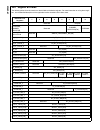
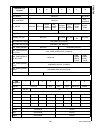
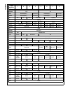
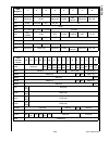
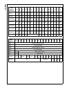
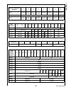
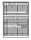
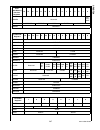
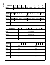
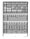
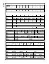
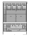
Www.National.Com 230 cp3bt26 29.0 register bit fields the following tables show the functions of the bit fields of the device registers. For more information on using these regis- ters, see the detailed description of the applicable function elsewhere in this data sheet. Bluetooth llc registers 7 6 ...
Page 231
231 www.National.Com cp3 bt26 wtptc_5slot[15:8] wtptc_5slot[15:8] seq_reset reserved seq_reset seq_continue reserved seq_ continue rx_status reserved hec error header error correction am_ addr error payload crc error payload error correction payload length error packet_ done chip_id reserved chip_id...
Page 232
Www.National.Com 232 cp3bt26 nakev out in nakmsk out in fwev rxwarn[3:1] reserved txwarn[3:1] reserved fwmsk rxwarn[3:1] reserved txwarn[3:1] reserved fnh mf ul rfc reserved fn[10:8] fnl fn[7:0] dmacntrl den ignrxtgl dtgl adma dmod dsrc dmaev reserved ntgl ardy dsiz dcnt derr dshlt dmamsk reserved d...
Page 233
233 www.National.Com cp3 bt26 rxs2 rx_err setup toggle rx_last rcount rxc2 reserved rfwl reserved flush ign_ setup reserved rx_en epc5 stall reserved iso ep_en ep txd3 txfd txs3 tx_urun ack_stat tx_done tcount txc3 ign_ isomsk tfwl rff flush toggle last tx_en epc6 stall reserved iso ep_en ep rxd3 rx...
Page 234
Www.National.Com 234 cp3bt26 can memory registers 15 14 13 12 11 10 9 8 7 6 5 4 3 2 1 0 cmbn.Id1 xi28 id10 xi27 id9 xi26 id8 xi25 id7 xi24 id6 xi23 id5 xi22 id4 xi21 id3 xi20 id2 xi19 id1 xi18 id0 srr rtr ide xi17 xi16 xi15 cmbn.Id0 xi14 xi13 xi12 xi11 xi10 xi9 xi8 xi7 xi6 xi5 xi4 xi3 xi2 xi1 xi0 rt...
Page 235
235 www.National.Com cp3 bt26 system configuration registers 7 6 5 4 3 2 1 0 mcfg reserved mem_io_ speed misc_io_ speed usb_ enable sclkoe mclkoe pllclkoe exioe dbgcfg reserved freeze on mstat isprst wdrst reserved dpgm busy pgmbusy oenv2 oenv1 oenv0 biu registers 15 12 11 10 9 8 7 6 5 4 3 2 1 0 bcf...
Page 236
Www.National.Com 236 cp3bt26 fmprog reserved ftprog fmperase reserved ftper fmmerase0 reserved ftmer fmend reserved ftend fmmend reserved ftmend fmrcv reserved ftrcv fmar0 reserved usb_ en- able fmar1 wrprot rdprot ispe empty bootarea fmar2 cadr15:0 flash program memory interface registers 15 14 13 ...
Page 237
237 www.National.Com cp3 bt26 fsmar0 reserved usb_ en- able fsmar1 wrprot rdprot ispe empty bootarea fsmar2 cadr15:0 flash data memory interface registers 15 14 13 12 11 10 9 8 7 6 5 4 3 2 1 0 cvsd/pcm registers 15 14 13 12 11 10 9 8 7 6 5 4 3 2 1 0 cvsdin cvsdin cvsdout cvsdout pcmin pcmin pcmout p...
Page 238
Www.National.Com 238 cp3bt26 pmm register 7 6 5 4 3 2 1 0 pmmcr hcch hccm dhc dmc wbpsm halt idle psm pmmsr reserved ohc omc olc miwu16 registers 15 14 13 12 11 10 9 8 7 6 5 4 3 2 1 0 wkedg wked wkena wken wkictl1 wkintr7 wkintr6 wkintr5 wkintr4 wkintr3 wkintr2 wkintr1 wkintr0 wkictl2 wkintr15 wkint...
Page 239
239 www.National.Com cp3 bt26 atdr1 atdh atdl atdr2 atdh atdl atdr3 atdh atdl agcr clk en aai en iom2 ifs fsl ctf crf iebc fss iefs scs lpb dwl ass aiscr reserved tx eic tx ic rx eic rx ic tx eip tx ip rx eip rx ip tx eie tx ie rx eie rx ie arscr rxfwm rxdsa rxsa rxo rxe rxf rx af atscr txfwm txdsa ...
Page 240
Www.National.Com 240 cp3bt26 mwspi16 registers 15 . . . 9 8 7 6 5 4 3 2 1 0 mwdat mwdat mwctl1 scdv scidl scm eiw eir eio echo mod mns mwen mwstat reserved ovr rbf bsy acb registers 7 6 5 4 3 2 1 0 acbsda data acbst slvstp sdast ber negack stastr nmatch master xmit acbcst arpmatch matchaf tgscl tsda...
Page 241
241 www.National.Com cp3 bt26 vtu registers 15 14 13 12 11 10 9 8 7 6 5 4 3 2 1 0 mode tmod4 t8 run t7 run tmod3 t6 run t5 run tmod2 t4 run t3 run tmod1 t2 run t1 run io1ctl p4 pol c4edg p3 pol c3edg p2 pol c2edg p1 pol c1edg io2ctl p7 pol c7edg p6 pol c6edg p5 pol c5edg p5 pol c5edg intctl i4den i4...
Page 242
Www.National.Com 242 cp3bt26 rng registers 15 14 13 12 11 10 9 8 7 6 5 4 3 2 1 0 rngcst reserved imsk reserved dvalid rnge rngd rngd rngdivh reserved rngdiv17:16 rngdivl rngdiv15:0
Page 243
243 www.National.Com cp3 bt26 30.0 electrical characteristics 30.1 absolute maximum ratings if military/aerospace specified devices are required, please contact the national semiconductor sales office/distribu- tors for availability and specifications. Note: absolute maximum ratings indicate limits ...
Page 244
Www.National.Com 244 cp3bt26 i o(off) output leakage current (i/o pins in input mode) 0v ≤ vout ≤ vcc -2.0 2.0 µa icca1 digital supply current active mode b vcc = 2.75v, iovcc=3.63v 20 ma iccprog digital supply current active mode c vcc = 2.75v, iovcc = 3.63v 20 ma iccps digital supply current power...
Page 245
245 www.National.Com cp3 bt26 30.3 usb transceiver electrical characteristics (temperature: -40°c ≤ t a ≤ +85°c) 30.4 adc electrical characteristics (temperature: -40°c ≤ t a ≤ +85°c) symbol parameter conditions min max units v di differential input sensitivity (d+) - (d-) -0.2 0.2 v v cm differenti...
Page 246
Www.National.Com 246 cp3bt26 30.5 flash memory on-chip programming symbol parameter conditions min max units t start program/erase to nvstr setup time a (nvstr = non-volatile storage a. Program/erase to nvstr setup time is determined by the following equation: t start = t clk × (ftdiv + 1) × (ftstar...
Page 247
247 www.National.Com cp3 bt26 30.6 output signal levels all output signals are powered by the digital supply (vcc). Table 83 summarizes the states of the output signals during the reset state (when vcc power exists in the reset state) and during the power save mode. The reset and nmi input pins are ...
Page 248
Www.National.Com 248 cp3bt26 figure 110. Clock timing figure 111. Nmi signal timing figure 112. Non-power-on reset figure 113. Power-on reset x1cki t x1h t x1l t x1p x2cki t x2h t x2l t x2p ds095 clk t iw t lh t ls nmi ds096 clk t rst reset ds097 vcc 0.9 vcc 0.1 vcc t ds115 r.
Page 249
249 www.National.Com cp3 bt26 30.8 uart timing figure 114. Uart asynchronous mode timing table 85 uart signals symbol figure description reference min (ns) max (ns) uart input signals t is 114 input setup time rxd (asynchronous mode) before rising edge (re) on clk - t ih 114 input hold time rxd (asy...
Page 250
Www.National.Com 250 cp3bt26 30.9 i/o port timing figure 115. I/o port timing table 86 i/o port signals symbol figure description reference min (ns) max (ns) i/o port input signals t is 115 input setup time before rising edge (re) on system clock - t ih 115 input hold time after re on system clock -...
Page 251
251 www.National.Com cp3 bt26 30.10 advanced audio interface (aai) timing figure 116. Receive timing, short frame sync table 87 advanced audio interface (aai) signals symbol figure description reference min (ns) max (ns) aai input signals t rds 116, 118 receive data setup time before falling edge (f...
Page 252
Www.National.Com 252 cp3bt26 figure 117. Transmit timing, short frame sync figure 118. Receive timing, long frame sync figure 119. Transmit timing, long frame sync 0 std sck sfs ds117 1 0 1 2 t tdv 0 srd srclk srfs ds118 1 0 1 2 t fsvh t fsvl t rdh t rds n 0 std sck sfs ds119 1 0 1 2 t tdv n.
Page 253
253 www.National.Com cp3 bt26 30.11 microwire/spi timing table 88 microwire/spi signals symbol figure description reference min (ns) max (ns) microwire/spi input signals t mskh 120 microwire clock high at 2.0v (both edges) 80 - t mskl 120 microwire clock low at 0.8v (both edges) 80 - t mskp 120 micr...
Page 254
Www.National.Com 254 cp3bt26 figure 120. Microwire transaction timing, normal mode, scidl = 0 t mdov 120 microwire data out valid normal mode: after fe on msk 25 alternate mode: after re on msk t mitop 124 mdodi to mdido (slave only) propagation time value is the same in all clocking modes of the mi...
Page 255
255 www.National.Com cp3 bt26 figure 121. Microwire transaction timing, normal mode, scidl = 1 lsb msb t mskp t mskh t mdlh t mdls t mcss t mcsh t msks t mdof t mdov t mdof t mdoh data in msk lsb msb mdodo (master) lsb msb mdido (slave) t mskh mcs (slave) t mskhd ds102.
Page 256
Www.National.Com 256 cp3bt26 figure 122. Microwire transaction timing, alternate mode, scidl = 0 msk lsb msb data in lsb msb mdodo (master) lsb msb mdido (slave) mcs (slave) t mskp t mskh t mdlh t mdls t mcss t mcsh t msks t mdof t mdov t mdof t mdoh t mskl t mskhd ds103.
Page 257
257 www.National.Com cp3 bt26 figure 123. Microwire transaction timing, alternate mode, scidl = 1 figure 124. Microwire transaction timing, data echoed to output, normal mode, scidl = 0, echo = 1, slave mode lsb msb t mskp t mskh t mdlh t mdls t mcss t skd t mcsh t msks t mdof t mdov t mdoff t mdoh ...
Page 258
Www.National.Com 258 cp3bt26 30.12 access.Bus timing table 89 access.Bus signals symbol figure description reference min (ns) max (ns) access.Bus input signals t bufi 126 bus free time between stop and start condition t sclhigho - t cstosi 126 scl setup time before stop condition (8 × t clk ) - t sc...
Page 259
259 www.National.Com cp3 bt26 figure 125. Acb signals (sda and scl) timing figure 126. Acb start and stop condition timing figure 127. Acb start condition timing scl 0.7vcc note: in the timing tables the parameter name is added with an "o" for output signal timing and "i" for input signal timing. 0....
Page 260
Www.National.Com 260 cp3bt26 figure 128. Acb data timing t scavo t sdah t csllow t sdasi t sclhigh scl sda note: in the timing tables the parameter name is added with an "o" for output signal timing and "i" for input signal timing. Unless the parameter already includes the suffix. Ds109.
Page 261
261 www.National.Com cp3 bt26 30.13 usb port ac characteristics 30.14 multi-function timer (mft) timing figure 129. Multi-function timer input timing table 90 usb port signals symbol description conditions a min typ max units t r rise time c l = 50 pf 4 20 ns t f fall time c l = 50 pf 4 20 ns t rfm ...
Page 262
Www.National.Com 262 cp3bt26 30.15 versatile timing unit (vtu) timing figure 130. Versatile timing unit input timing table 92 versatile timing unit input signals symbol figur e description reference min (ns) max (ns) t tioh 129 tiox input high time rising edge (re) on clk 1.5 × t clk + 5ns t tiol 12...
Page 263
263 www.National.Com cp3 bt26 30.16 external bus timing table 93 external bus signals symbol figure description reference min (ns) max (ns) external bus input signals t 1 131, 133, 134, 135 input setup time d[15:0] before rising edge (re) on clk 8 t 2 131, 133, 134, 135 output hold time d[15:0] afte...
Page 264
Www.National.Com 264 cp3bt26 figure 131. Early write between normal read cycles (no wait states) t1 t2 t1 t2 t3 t1 t2 a[21:0] a22 ('13 only) clk normal read normal read early write selx d[15:0] in in out t 4 t 4 , t 12 sely (y ≠ x) rd wr[1:0] t 5 , t 12 t 5 , t 12 t 5 , t 12 t 8 , t 12 t 3 t 9 t 5 ,...
Page 265
265 www.National.Com cp3 bt26 figure 132. Late write between normal read cycles (no wait states) t1 t2 t1 t2 t1 t2 clk selx d[15:0] in in out (y ≠ x) rd normal read normal read late write t 4 , t 12 t 5 , t 12 t 5 , t 12 t 5 , t 12 t 5 , t 12 t 8 , t 12 t 3 t 11 t 5 , t 12 t 6 , t 13 t 6 , t 13 t 5 ...
Page 266
Www.National.Com 266 cp3bt26 figure 133. Consecutive normal read cycles (burst, no wait states) t1 t2 t2b t1 t2 t2b normal read normal read clk selx sely wr[1:0] d[15:0] in in in in (y ≠ x) (y ≠ x) rd t 5 , t 12 t 5 , t 12 t 4 , t 12 t 4 , t 12 t 4 t 5 , t 12 t 5 , t 12 t 7 t 5 , t 12 t 5 , t 12 t 2...
Page 267
267 www.National.Com cp3 bt26 figure 134. Normal read cycle (wait cycle followed by hold cycle) t1 tw t2 th clk d[15:0] seln, selio wr[1:0] rd t 4 t 5 , t 12 t 5 , t 12 t 5 , t 12 t 5 , t 12 t 2 t 1 t 4 , t 12 a21:0 a22 ('13 only) bus state ds127.
Page 268
Www.National.Com 268 cp3bt26 figure 135. Early write between fast read cycles t idle t1-2 t1 t1 t2 t3 t1-2 fast read early write clk selx sely wr[1:0] d[15:0] (y ≠ x) (y ≠ x) rd fast read t 5 , t 12 t 5 , t 12 t 2 t 1 t 5 , t 12 t 5 , t 12 t 4 , t 12 t 4 a[21:0] a22 ('13 only) bus state ds128 in in ...
Page 269
269 www.National.Com cp3 bt26 31.0 pin assignments 31.1 lqfp-128 package for 128-pin devices, figure 136 provides a pinout diagram, and table 94 provides the pin assignments. The physical di- mensions are provided in section 33.0. Figure 136. Cp3bt26 in the lqfp-128 package (top view) ds181 cp3bt26 ...
Page 270
Www.National.Com 270 cp3bt26 avcc 29 pwr adgnd 90 pwr advcc 89 pwr uvcc 62 pwr ugnd 63 pwr x2cki 30 i x2cko 31 o env2 slowclk 34 i/o env1 cpuclk 35 i/o env0 pllclk 36 i/o reset 100 i tms 101 i tdi 102 i tck 103 i tdo 106 o rdy 108 o rfdata 68 i/o d- 61 i/o d+ 60 i/o scl 81 i/o sda 82 i/o adc0 tsx+ 9...
Page 271
271 www.National.Com cp3 bt26 pc5 d13 5 gpio pc6 d14 3 gpio pc7 d15 2 gpio pe0 rxd0 87 gpio pe1 txd0 83 gpio pe2 rts 86 gpio pe3 cts 88 gpio pe4 ckx/tb 40 gpio pe5 srfs/nmi 120 gpio pf0 msk/tio1 111 gpio pf1 mdido/tio2 114 gpio pf2 mdodi/tio3 116 gpio pf3 mwcs/tio4 109 gpio pf4 sck/tio5 122 gpio pf5...
Page 272
Www.National.Com 272 cp3bt26 31.2 lqfp-144 package for 144-pin devices, figure 137 provides a pinout diagram, and table 95 provides the pin assignments. The physical di- mensions are provided in section 33.0. Figure 137. Cp3bt26 in the lqfp-144 package (top view) ds182 1 pc7 pc6 iognd pc5 pc4 iovcc ...
Page 273
273 www.National.Com cp3 bt26 table 95 pin assignments for lqfp-144 package pin name alternate function(s) pin number type gnd 23, 32, 58, 85, 91, 121 pwr vcc 24, 31, 57, 86, 90, 122 pwr iognd 3, 9, 16, 43, 46, 49, 55, 66, 84, 117, 130 pwr iovcc 6, 12, 20, 41, 44, 51, 63, 80, 126, 140 pwr agnd 27 pw...
Page 274
Www.National.Com 274 cp3bt26 pb4 d4 17 gpio pb5 d5 15 gpio pb6 d6 14 gpio pb7 d7 13 gpio pc0 d8 11 gpio pc1 d9 10 gpio pc2 d10 8 gpio pc3 d11 7 gpio pc4 d12 5 gpio pc5 d13 4 gpio pc6 d14 2 gpio pc7 d15 1 gpio pe0 rxd0 93 gpio pe1 txd0 89 gpio pe2 rts 92 gpio pe3 cts 94 gpio pe4 ckx/tb 37 gpio pe5 sr...
Page 275
275 www.National.Com cp3 bt26 a22 62 o a21 61 o a20 60 o a19 54 o a18 53 o a17 45 o a16 42 o a15 40 o a14 39 o a13 143 o a12 142 o a11 141 o a10 139 o a9 132 o a8 131 o a7 129 o a6 128 o a5 125 o a4 124 o a3 119 o a2 118 o a1 116 o a0 114 o sel0 79 o sel1 81 o sel2 82 o selio 83 o rd 65 o wr0 67 o w...
Page 276
Www.National.Com 276 cp3bt26 32.0 revision history table 96 revision history date major changes from previous version 4/3/03 original release. 5/26/03 fixed maximum boot area in section 8. Fixed names of clock signals in figures 5 and 6. Fixed addresses of fsmarx registers in register map section. A...
Page 277
277 www.National.Com cp3 bt26 33.0 physical dimensions (millimeters) unless otherwise noted figure 138. Lqfp-128 package figure 139. Lqfp-144 package.
Page 278
National semiconductor americas customer support center email: new.Feedback@nsc.Com tel: 1-800-272-9959 national semiconductor europe customer support center fax: +49 (0) 180-530 85 86 email: europe.Support@nsc.Com deutsch tel: +49 (0) 69 9508 6208 english tel: +44 (0) 870 24 0 2171 français tel: +3...

