- DL manuals
- National Instruments
- Transceiver
- NI 5791R
- User Manual And Specifications
National Instruments NI 5791R User Manual And Specifications
USER MANUAL AND SPECIFICATIONS
NI 5791R
RF Transceiver Adapter Module
The NI 5791 is an RF transceiver adapter module designed to work in conjunction with your
NI FlexRIO
™
FPGA module. The NI 5791 features the following connectors and chips:
•
2-channel, 130 MS/s analog-to-digital converter (ADC) with 14-bit accuracy
•
2-channel, 130 MS/s (520 MS/s after interpolation) digital-to-analog converter (DAC)
with 16-bit accuracy
•
LO input and LO output connectors to support LO sharing for multiple-channel
applications
•
Timing chip with clocking options from the backplane and the front panel
•
Programmable attenuators
•
Selectable receive and transmit filters
•
The following front panel connectors:
–
RX IN
–
LO OUT
–
CLK IN
–
CLK OUT
–
LO IN
–
TX OUT
The NI 5791 can upconvert and downconvert RF signals ranging from 200 MHz to 4.4 GHz.
This document contains signal information and lists the specifications of the NI 5791R, which
is composed of the NI FlexRIO FPGA module and the NI 5791. This document also contains
Summary of NI 5791R
Page 1
User manual and specifications ni 5791r rf transceiver adapter module the ni 5791 is an rf transceiver adapter module designed to work in conjunction with your ni flexrio ™ fpga module. The ni 5791 features the following connectors and chips: • 2-channel, 130 ms/s analog-to-digital converter (adc) w...
Page 2
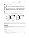
Tutorial sections that demonstrate how to acquire data using a labview fpga example vi and how to create and run your own labview project with the ni 5791r. Note ni 5791r refers to the combination of your ni 5791 adapter module and your ni flexrio fpga module. Ni 5791 refers to your ni 5791 adapter ...
Page 3
Using your ni 5791r with a labview fpga example vi.................................................13 using the included streaming example..........................................................................14 creating a labview project..............................................................
Page 4
Furthermore, any modifications to the product not expressly approved by national instruments could void your authority to operate it under your local regulatory rules. Caution to ensure the specified emc performance, operate this product only with shielded cables and accessories. Caution to ensure t...
Page 5
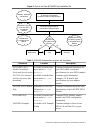
Figure 2. How to use your ni flexrio documentation set. Labview fpga module help ni flexrio help labview examples install hardware and software connect signals and learn about your adapter module learn about labview fpga module program your ni flexrio system in labview fpga module ni flexrio fpga mo...
Page 6
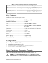
Table 1. Ni flexrio documentation locations and descriptions (continued) document location description ipnet ni.Com/ipnet contains labview fpga functions and intellectual property to share. Ni flexrio product page ni.Com/flexrio contains product information and data sheets for ni flexrio devices. Ke...
Page 7
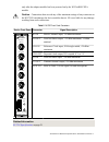
Only after the adapter module has been powered on by the ni flexrio fpga module. Caution connections that exceed any of the maximum ratings of any connector on the ni 5791r can damage the device and the chassis. Ni is not liable for any damage resulting from such connections. Table 2. Ni 5791 front ...
Page 8
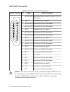
Aux i/o connector table 3. Ni 5791 aux i/o connector pin assignments aux i/o connector pin signal signal description 18 16 14 12 10 8 6 4 2 19 17 1 3 5 7 9 11 13 15 1 dio port 0 (0) bidirectional single-ended (se) digital i/o (dio) data channel. 2 gnd ground reference for signals. 3 dio port 0 (1) b...
Page 9
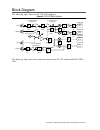
Block diagram the following figure shows the ni 5791 block diagram. Figure 3. Ni 5791 block diagram adc 14 bit ti ads4246 noise reject lpf 4.4 ghz lpf 4.4 ghz lpf tx rf filter bank 44 mhz hpf noise reject lpf 52 mhz lpf 204 mhz lpf 204 mhz lpf 52 mhz lpf tx lo filter bank adc 14 bit ti ads4246 dac 1...
Page 10
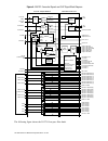
Figure 4. Ni 5791 connector signals and clip signal block diagram ni 5791 adapter module from rf mixer to rf mixer dio port 0 (0) from rf lo rf filters rf lo and attenuators spi dio port 0 (1) dio port 0 (2) dio port 0 (3) dio port 1 (0) dio port 1 (1) dio port 1 (2) dio port 1 (3) pfi 0 pfi 1 pfi 2...
Page 11
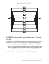
Figure 5. Low-pass filter (lpf) bank 3600 mhz lpf 2400 mhz lpf 1600 mhz lpf 1066 mhz lpf 711 mhz lpf 474 mhz lpf 316 mhz lpf 4400 mhz lpf ni 5791 component-level intellectual property (clip) the labview fpga module includes component-level intellectual property (clip) for hdl ip integration. Ni flex...
Page 12
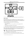
Figure 6. Clip and fpga vi relationship adapter module clip socket labview fpga vi user-defined clip ni flexrio fpga module fpga exter nal i/o connector adapter module socketed clip user-defined clip fixed i/o dram 0 clip socket socketed clip dram 1 clip socket socketed clip fix ed i/o fix ed i/o dr...
Page 13
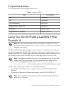
Programmable chips you can program the following chips from the clip. Table 4. Programmable chips chip part number adc ti ads4246 dac ti dac3482 clock distribution adi ad9511 frequency/phase adjust dac adi ad5541 eeprom sst25vf080b programmable rf attenuator peregrine pe43703 using your ni 5791r wit...
Page 14
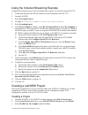
Using the included streaming example complete the following steps to run an example that acquires a waveform using the ni 5791. 1. Connect an antenna to the rx in connector on the front panel of the ni 5791. 2. Launch labview. 3. Select file»open project. 4. Navigate to \examples\instri579x\stream...
Page 15
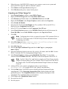
4. Either discover a labview fpga target in your system or create a new system and specify an fpga target for which to construct a project. 5. Click finish in the project preview dialog box. 6. Click file»save and specify a name for the project. Creating an fpga target vi 1. In the project explorer ...
Page 16
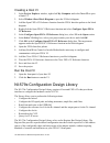
Creating a host vi 1. In the project explorer window, right-click my computer and select new»vi to open a blank vi. 2. Select window»show block diagram to open the vi block diagram. 3. Add the open fpga vi reference function from the fpga interface palette to the block diagram. 4. Right-click the op...
Page 17
The ni-579x configuration design library host vis all require a register bus object for the device you want to configure. Create the register bus object using open session.Vi, or use ni579x open.Vi. For more information about how to use the ni-579x configuration design library, refer to the example ...
Page 18
Devices are ±180 degrees out of phase. If the devices are zero degrees out of phase, device alignment offset is also zero degrees. Note for the best synchronization results, minimize the phase offset between devices. Caution before attempting to synchronize your ni flexrio devices, notice the follow...
Page 19
Host-driven synchronization host-driven synchronization allows you to perform the following actions: • decouple the sample clock and the reference clock • use an external sample clock • set the cptr period manually host-driven synchronization requires an additional fpga i/o line and host involvement...
Page 20
The edge is synchronized at the next cptr edge. After all the device cptrs are aligned, an edge sent out on the fpga i/o lines is read at the same clock cycle across all the devices. Note the quality of synchronization is only as good as the quality of sample clock locking. Some static skew may exis...
Page 21
– run the synchronization vi. – refer to the example fpga code at \examples\instri579x\streaming . • fpga vi: – configure the cptr period. The synchronization library ensures that the cptr period is the same on the host and the fpga. – refer to the example fpga code at \examples\instri579x\strea...
Page 22
Information about rf device applications, visit to contact a national instruments branch office. Specifications describe the warranted product performance over ambient temperature ranges of 0 °c to 55 °c, unless otherwise noted. Specifications are subject to change without notice. For the most recen...
Page 23
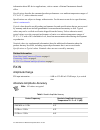
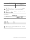
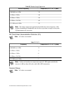
Table 6. Absolute amplitude accuracy (continued) center frequency absolute amplitude accuracy, temperature 23 °c ± 5 °c (db) >3 ghz to 3.9 ghz 1.3 >3.9 ghz to 4.4 ghz 1.5 note absolute amplitude accuracy uses a correction coefficient in eeprom to improve performance. Performance is verified over the...
Page 24
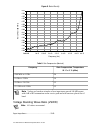
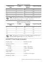
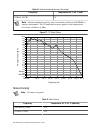
Figure 9. Noise density frequency (hz) noise floor (dbm/hz) –168 –167 –166 –165 –164 –163 –162 –161 –160 –159 –158 –157 –156 –155 –154 –153 1.0 g 1.50 g 2.0 g 2.5 g 3.0 g 3.5 g 4.0 g 4.4 g 200.0 m table 8. Gain compression (nominal) frequency gain compression, temperature 23 °c ± 5 °c (dbm) >200 mhz...
Page 25
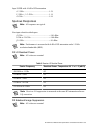
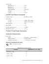
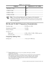
Input vswr with 10 db of rx attenuation .................................................................... 1.5:1 .................................................................... 1.3 ghz f 1.1:1 .................................................................... >3 ghz 1.9:1 spurious responses...
Page 26
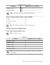
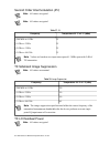
Table 10. Sideband image suppression center frequency temperature 23 °c ± 5 °c (dbc) >200 mhz to 1 ghz -39 >1 ghz to 2 ghz -58 >2 ghz to 3 ghz -54 >3 ghz to 3.9 ghz -45 >3.9 ghz to 4.4 ghz -35 note the image suppression specifications hold at the center frequency of the acquired instantaneous bandwi...
Page 27
Table 12. Dynamic range at 900 mhz reference level (dbm) ip 3 (dbm) noise floor (dbm/hz) dynamic range (db) 5 24 -135 106 -5 14 -145 106 -15 4 -155 106 -25 0 -163 109 note the signal level of each tone is set to 6 db less than the reference level to prevent overload. Dynamic range = 2/3 × (imd 3 – n...
Page 28
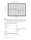
Figure 10. Lo output power 0 1 2 3 4 5 6 7 8 9 10 1e+09 500 m 1.5e+09 2e+09 2.5e+09 3e+09 3.5e+09 4e+09 4.5e+09 5e+09 0 lo frequency (hz) lo output p ow er (dbm) note for frequencies above 2.8 ghz, the gain is chain up to eight channels of adapter modules below 2.8 ghz without external amplification...
Page 29
Interface logic .................................................................... Maximum v ol 0.55 v .................................................................... Minimum v oh 2.7 v .................................................................... Maximum v oh 3.6 v ......................
Page 30
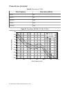
Table 14. Absolute amplitude accuracy (continued) frequency temperature 23 °c ±5 °c (db) 3 ghz to 4.4 ghz 1.8 note absolute amplitude accuracy uses a correction coefficient in eeprom to improve performance. The tx amplitude accuracy applies to the output power level from -12 dbm to -4 dbm. Figure 11...
Page 31
Table 15. Noise density (continued) frequency temperature 23 °c ±5 °c (dbm/hz) >2 ghz to 3 ghz -130 >3 ghz to 4.4 ghz -130 note performance is measured with 0 db of tx attenuation. Output voltage standing wave ratio (vswr) ............................................................................ ...
Page 32
Second order intermodulation (ip 2 ) note all values are typical. Note all values are typical. Table 17. Ip 2 frequency temperature 23 °c ±5 °c (dbm) >200 mhz to 1 ghz 25 >1 ghz to 2 ghz 25 >2 ghz to 3 ghz 25 >3 ghz to 4.4 ghz 35 note values are based on two input tones spaced 1.3 mhz apart with 5 d...
Page 33
Table 19. Tx lo residual power frequency temperature 23 °c ±5 °c (dbm) >200 mhz to 1 ghz -48 >1 ghz to 2 ghz -48 >2 ghz to 3 ghz -48 >3 ghz to 4.4 ghz -45 note this specification holds at the center frequency of the transmitted instantaneous bandwidth, 100 mhz maximum after the device performs a rec...
Page 34
Phase noise (nominal) table 20. Phase noise at 2.4 ghz offset frequency phase noise (dbc/hz) 1 khz -90 10 khz -94 100 khz -104 1 mhz -130 10 mhz -140 figure 12. Phase noise (900 mhz, 2.4 ghz, 4.4 ghz) offset frequency (hz) phase noise (dbc/hz) –90 –80 –100 –70 –50 –60 –110 –130 –120 –140 –40 100 1 k...
Page 35
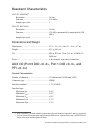
Baseband characteristics adc (ti ads4246) 4 .................................................................... Resolution 14 bits .................................................................... Data rate 130 ms/s 5 .................................................................... Samples p...
Page 36
.................................................................... Z out 50 Ω ± 20% .................................................................... I out (dc) ±2 ma ............................................................................ Pull-down resistor 150 kΩ ............................
Page 37
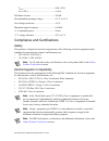
Ce compliance this product meets the essential requirements of applicable european directives, as follows: • 2006/95/ec; low-voltage directive (safety) • 2004/108/ec; electromagnetic compatibility directive (emc) online product certification to obtain product certifications and the doc for this prod...
Page 38
Operating environment ............................................................................ Ambient temperature range 0 °c to 55 °c (tested in accordance with iec-60068-2-1 and iec-60068-2-2.) ............................................................................ Relative humidity range...
Page 39
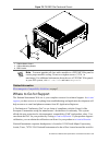
Figure 13. Pxi emc filler panels and chassis 1 1 3 2 1. Captive screw covers 2. Captive mounting screws 3. Emc gasket note you must populate all slots with a module or a pxi emc filler panel to ensure proper module cooling. Do not over tighten screws (2.5 lb · in maximum). For additional information...
Page 40
Help address your support needs. For telephone support in the united states, create your service request at ni.Com/support and follow the calling instructions or dial 512 795 8248. For telephone support outside the united states, visit the worldwide offices section of ni.Com/ niglobal to access the ...

