- DL manuals
- National Instruments
- Computer Hardware
- PCI-6503
- User Manual
National Instruments PCI-6503 User Manual
Summary of PCI-6503
Page 1
Daq pci-dio-96/pxi-6508/pci-6503 user manual 96-bit and 24-bit parallel digital i/o interface for pci, pxi, and compactpci pci-dio-96/pxi-6508/pci-6503 user manual march 2009 374938b-01.
Page 2
Support worldwide technical support and product information ni.Com national instruments corporate headquarters 11500 north mopac expressway austin, texas 78759-3504 usa tel: 512 683 0100 worldwide offices australia 1800 300 800, austria 43 662 457990-0, belgium 32 (0) 2 757 0020, brazil 55 11 3262 3...
Page 3: Important Information
Important information warranty the pci-dio-96, pxi-6508, and pci-6503 are warranted against defects in materials and workmanship for a period of one year from the date of shipment, as evidenced by receipts or other documentation. National instruments will, at its option, repair or replace equipment ...
Page 4: Contents
© national instruments corporation v pci-dio-96/pxi-6508/pci-6503 user manual contents about this manual conventions ...................................................................................................................Ix related documentation...............................................
Page 5
Contents pci-dio-96/pxi-6508/pci-6503 user manual vi ni.Com chapter 4 theory of operation functional overview ..................................................................................................... 4-1 pci interface circuitry................................................................
Page 6
Contents © national instruments corporation vii pci-dio-96/pxi-6508/pci-6503 user manual port c status-word bit definitions for bidirectional data path (port a only) .................................................................B-27 interrupt handling ................................................
Page 7
Contents pci-dio-96/pxi-6508/pci-6503 user manual viii ni.Com figure b-10. Control word to configure port a as mode 2 bidirectional data bus .......................................................................... B-26 figure b-11. Port c pin assignments on i/o connector when port c is configured ...
Page 8: About This Manual
© national instruments corporation ix pci-dio-96/pxi-6508/pci-6503 user manual about this manual this manual describes the electrical and mechanical aspects of the pci-dio-96, pxi-6508, and pci-6503 and contains information concerning their installation, operation, and programming. The pci-dio-96 an...
Page 9: Related Documentation
About this manual pci-dio-96/pxi-6508/pci-6503 user manual x ni.Com monospace text in this font denotes text or characters that you should enter from the keyboard, sections of code, programming examples, and syntax examples. This font is also used for the proper names of disk drives, paths, director...
Page 10: Introduction
© national instruments corporation 1-1 pci-dio-96/pxi-6508/pci-6503 user manual 1 introduction this chapter describes the pci-dio-96, pxi-6508, and pci-6503; lists what you need to get started, software programming choices, and optional equipment; describes custom cabling options; and explains how t...
Page 11: Using Pxi With Compactpci
Chapter 1 introduction pci-dio-96/pxi-6508/pci-6503 user manual 1-2 ni.Com using pxi with compactpci using pxi-compatible products with standard compactpci products is an important feature provided by the pxi specification , revision 1.0. If you use a pxi-compatible plug-in device in a standard comp...
Page 12: Optional Equipment
Chapter 1 introduction © national instruments corporation 1-3 pci-dio-96/pxi-6508/pci-6503 user manual optional equipment national instruments offers a variety of products to use with your dio board, including cables, connector blocks, and other accessories, as follows: • cables and cable assemblies...
Page 13: Unpacking
Chapter 1 introduction pci-dio-96/pxi-6508/pci-6503 user manual 1-4 ni.Com the mating connector for the pci-6503 is a 50-position, polarized ribbon socket connector with strain relief. National instruments uses a polarized (keyed) connector to prevent inadvertent upside-down connections. Recommended...
Page 14: Software Installation
© national instruments corporation 2-1 pci-dio-96/pxi-6508/pci-6503 user manual 2 installation and configuration this chapter describes how to install and configure your pci-dio-96, pxi-6508, or pci-6503 board. Software installation before installing your dio device, you must install the software yo...
Page 15: Board Configuration
Chapter 2 installation and configuration pci-dio-96/pxi-6508/pci-6503 user manual 2-2 ni.Com 3. Remove the expansion slot cover on the back panel of the computer. 4. Touch the metal part inside your computer to discharge any static electricity that might be on your clothes or body. 5. Insert the pci...
Page 16: Signal Connections
© national instruments corporation 3-1 pci-dio-96/pxi-6508/pci-6503 user manual 3 signal connections this chapter describes how to make input and output signal connections to your pci-dio-96, pxi-6508, and pci-6503 via the board i/o connector. Caution connections that exceed any of the maximum ratin...
Page 17
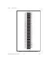
Chapter 3 signal connections pci-dio-96/pxi-6508/pci-6503 user manual 3-2 ni.Com figure 3-1. Pci-dio-96 and pxi-6508 connector pin assignments gnd +5 v bpa0 apa0 bpa1 apa1 bpa2 apa2 bpa3 apa3 bpa4 apa4 bpa5 apa5 bpa6 apa6 bpa7 apa7 bpb0 apb0 bpb1 apb1 bpb2 apb2 bpb3 apb3 bpb4 apb4 bpb5 apb5 bpb6 apb...
Page 18
Chapter 3 signal connections © national instruments corporation 3-3 pci-dio-96/pxi-6508/pci-6503 user manual cable assembly connectors the optional r1005050 cable assembly you can use with the pci-dio-96 or pxi-6508 is an assembly of two 50-pin cables and three connectors. Both cables are joined to ...
Page 19
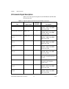
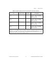
Chapter 3 signal connections pci-dio-96/pxi-6508/pci-6503 user manual 3-4 ni.Com i/o connector signal descriptions table 3-1 lists the signal descriptions for the pci-dio-96 and pxi-6508 i/o connector pins. Table 3-1. Signal descriptions for pci-dio-96 and pxi-6508 i/o connectors pin signal name alt...
Page 20
Chapter 3 signal connections © national instruments corporation 3-5 pci-dio-96/pxi-6508/pci-6503 user manual 67, 69, 71, 73, 75, 77, 79, 81 cpb 7 bidirectional data lines for port b of ppi c—cpb7 is the msb, cpb0 is the lsb. 68, 70, 72, 74, 76, 78, 80, 82 dpb 10 bidirectional data lines for port b o...
Page 21: I/o Connector (Pci-6503)
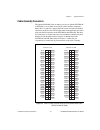
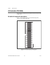
Chapter 3 signal connections pci-dio-96/pxi-6508/pci-6503 user manual 3-6 ni.Com i/o connector (pci-6503) the pci-6503 has 50 pins that you can connect to 50-pin accessories with the nb1 cable. Pci-6503 i/o connector pin descriptions figure 3-3 shows the pin assignments for the pci-6503 digital i/o ...
Page 22: Port C Pin Assignments
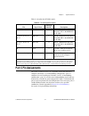
Chapter 3 signal connections © national instruments corporation 3-7 pci-dio-96/pxi-6508/pci-6503 user manual table 3-2 describes the pci-6503 signals. Port c pin assignments the signals assigned to port c vary depending on how the 82c55a is configured. In mode 0—or no handshaking configuration—port ...
Page 23
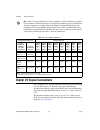
Chapter 3 signal connections pci-dio-96/pxi-6508/pci-6503 user manual 3-8 ni.Com note table 3-3 shows both the port c signal assignments and the terminology correlation between different documentation sources. The 82c55a terminology refers to the different 82c55a configurations as modes whereas ni-d...
Page 24
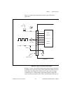
Chapter 3 signal connections © national instruments corporation 3-9 pci-dio-96/pxi-6508/pci-6503 user manual figure 3-4 depicts signal connections for three typical digital i/o applications. Figure 3-4. Digital i/o connections block diagram in figure 3-4, port a of one ppi is configured for digital ...
Page 25: Power Connections
Chapter 3 signal connections pci-dio-96/pxi-6508/pci-6503 user manual 3-10 ni.Com power connections pin 49 and, on the pci-dio-96 and pxi-6508, pin 99 of the i/o connector supply +5 v from the computer power supply via a self-resetting fuse. The fuse resets automatically within a few seconds after t...
Page 26
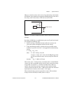
Chapter 3 signal connections © national instruments corporation 3-11 pci-dio-96/pxi-6508/pci-6503 user manual however, ensure the resistor value is not so large that leakage current from the dio line along with the current from the 100 k Ω pull-up resistor drives the voltage at the resistor above a ...
Page 27
Chapter 3 signal connections pci-dio-96/pxi-6508/pci-6503 user manual 3-12 ni.Com low dio power-up state (pxi-6508, pci-6503 only) if you select pulled-low mode, each dio line will be pulled to gnd (0 vdc) using a 100 k Ω resistor. If you want to pull a specific line high, connect a pull-up resistor...
Page 28
Chapter 3 signal connections © national instruments corporation 3-13 pci-dio-96/pxi-6508/pci-6503 user manual this resistor value, 5.7 k Ω , provides a maximum of 2.8 v on the dio line at power up. You can substitute smaller resistor values to lower the voltage drop or to provide a margin for v cc v...
Page 29: Theory of Operation
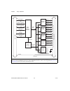
© national instruments corporation 4-1 pci-dio-96/pxi-6508/pci-6503 user manual 4 theory of operation this chapter contains a functional overview of the pci-dio-96, pxi-6508, and pci-6503 and explains the operation of each functional unit. Functional overview the block diagram in figure 4-1 illustra...
Page 30
Chapter 4 theory of operation pci-dio-96/pxi-6508/pci-6503 user manual 4-2 ni.Com figure 4-1. Pci-dio-96/pxi-6508 block diagram note : current revisions of the ni pci-dio-96 and pxi-6508 no longer support the oki 82c53 programmable interval timer. If you are using a pci-dio-96 revision g or earlier ...
Page 31
Chapter 4 theory of operation © national instruments corporation 4-3 pci-dio-96/pxi-6508/pci-6503 user manual pci interface circuitry your dio board uses the pci mite asic to communicate with the pci bus. The pci mite asic was designed by national instruments specifically for data acquisition. The p...
Page 32: Timing Specifications
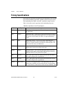
Chapter 4 theory of operation pci-dio-96/pxi-6508/pci-6503 user manual 4-4 ni.Com timing specifications this section lists the timing specifications for handshaking with your dio board. The handshaking lines stb* and ibf synchronize input transfers. The handshaking lines obf* and ack* synchronize ou...
Page 33
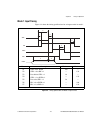
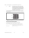
Chapter 4 theory of operation © national instruments corporation 4-5 pci-dio-96/pxi-6508/pci-6503 user manual mode 1 input timing figure 4-2 shows the timing specifications for an input transfer in mode 1. Figure 4-2. Timing specifications for mode 1 input transfer name description minimum † maximum...
Page 34
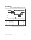
Chapter 4 theory of operation pci-dio-96/pxi-6508/pci-6503 user manual 4-6 ni.Com mode 1 output timing figure 4-3 shows the timing specifications for an output transfer in mode 1. Figure 4-3. Timing specifications for mode 1 output transfer name description minimum † maximum † t1 wr* = 0 to intr = 0...
Page 35
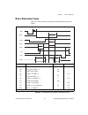
Chapter 4 theory of operation © national instruments corporation 4-7 pci-dio-96/pxi-6508/pci-6503 user manual mode 2 bidirectional timing figure 4-4 shows the timing specifications for bidirectional transfers in mode 2. Figure 4-4. Timing specifications for mode 2 bidirectional transfer name descrip...
Page 36: Specifications
© national instruments corporation a-1 pci-dio-96/pxi-6508/pci-6503 user manual a specifications this appendix lists the specifications for the pci-dio-96, pxi-6508, and pci-6503. These specifications are typical at 25 ° c unless otherwise noted. Digital i/o number of channels pci-dio-96 and pxi-650...
Page 37
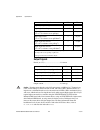
Appendix a specifications pci-dio-96/pxi-6508/pci-6503 user manual a-2 ni.Com output signals pin 49 (at +5 v) ......................................1.0 a max output current.........................................2.5 ma typ caution drawing more than the typical 2.5 ma current ( Ω load at 5 v output)...
Page 38
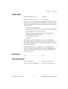
Appendix a specifications © national instruments corporation a-3 pci-dio-96/pxi-6508/pci-6503 user manual transfer rates max with ni-daq software .................. 50 kbytes/s constant sustainable rate (typ) ............... 1 to 10 kbytes/s transfer rates are a function of the speed with which your...
Page 39
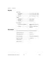
Appendix a specifications pci-dio-96/pxi-6508/pci-6503 user manual a-4 ni.Com physical dimensions pci-dio-96 .....................................13.7 × 10.7 cm (5.4 × 4.2 in.) pxi-6508 .........................................17.5 × 10.7 cm (6.9 × 4.2 in.) pci-6503.....................................
Page 40
Appendix a specifications © national instruments corporation a-5 pci-dio-96/pxi-6508/pci-6503 user manual shock and vibration functional shock (pxi-6508)................. Mil-t-28800 e class 3 (per section 4.5.5.4.1); half-sine shock pulse, 11 ms duration, 30 g peak, 30 shocks per face operational r...
Page 41: Rohs
Appendix a specifications pci-dio-96/pxi-6508/pci-6503 user manual a-6 ni.Com ce compliance this product meets the essential requirements of applicable european directives as follows: • 2006/95/ec; low-voltage directive (safety) • 2004/108/ec; electromagnetic compatibility directive (emc) online pro...
Page 42: Register-Level Programming
© national instruments corporation b-1 pci-dio-96/pxi-6508/pci-6503 user manual b register-level programming this appendix describes in detail the address and function of each pci-dio-96, pxi-6508, and pci-6503 register, contains instructions on how to operate dio board circuitry, and provides examp...
Page 43: (Pci-Dio-96, Pxi-6508 Only)
Appendix b register-level programming — 82c53 programmable interval timer (pci-dio-96, pxi-6508 only) pci-dio-96/pxi-6508/pci-6503 user manual b-2 ni.Com 82c53 programmable interval timer (pci-dio-96, pxi-6508 only) the pci-dio-96 and pxi-6508 contain an 82c53 programmable interval timer for use by ...
Page 44
Appendix b register-level programming — 82c53 programmable interval timer (pci-dio-96, pxi-6508 only) © national instruments corporation b-3 pci-dio-96/pxi-6508/pci-6503 user manual the block diagram in figure b-1 illustrates the interrupt control circuitry. Figure b-1. Interrupt control circuitry b...
Page 45: Register Map and Description
Appendix b register-level programming — register map and description pci-dio-96/pxi-6508/pci-6503 user manual b-4 ni.Com register map and description this section describes in detail the address and function of each pci-dio-96, pxi-6508, and pci-6503 register. Introduction the three 8-bit ports of t...
Page 46
Appendix b register-level programming — register map and description © national instruments corporation b-5 pci-dio-96/pxi-6508/pci-6503 user manual register map table b-1 lists the address map for your dio board. The pci-dio-96 and pxi-6508 use all of the registers. The pci-6503 uses a subset of th...
Page 47
Appendix b register-level programming — register map and description pci-dio-96/pxi-6508/pci-6503 user manual b-6 ni.Com register descriptions the following sections contain the register descriptions for the devices used on your dio board. The register description bits labeled with an x indicate res...
Page 48
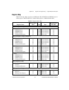
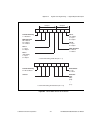
Appendix b register-level programming — register map and description © national instruments corporation b-7 pci-dio-96/pxi-6508/pci-6503 user manual figure b-2. Control word formats for the 82c55a d7 d6 d5 d4 d3 d2 d1 d0 group a group b mode selection 00 = mode 0 01 = mode 1 1x = mode 2 control word...
Page 49
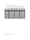
Appendix b register-level programming — register map and description pci-dio-96/pxi-6508/pci-6503 user manual b-8 ni.Com table b-2 shows the control words for setting or resetting each bit in port c. Notice that programming the set/reset option for the bits of port c clears bit 7 of the control word...
Page 50
Appendix b register-level programming — register map and description © national instruments corporation b-9 pci-dio-96/pxi-6508/pci-6503 user manual register description for the 82c53 (pci-dio-96, pxi-6508 only) figure b-3 shows the control word format used to program the 82c53. Bits 7 and 6 of the ...
Page 51
Appendix b register-level programming — interrupt control register 1 pci-dio-96/pxi-6508/pci-6503 user manual b-10 ni.Com register description for the interrupt control registers there are two interrupt control registers on your dio board. One of these registers has individual enable bits for the tw...
Page 52
Appendix b register-level programming — interrupt control register 1 © national instruments corporation b-11 pci-dio-96/pxi-6508/pci-6503 user manual 5 cirq1 ppi c port b interrupt enable bit—if this bit and the inten bit in interrupt control register 2 are both set, ppi c sends an interrupt, intrb,...
Page 53
Appendix b register-level programming — interrupt control register 2 pci-dio-96/pxi-6508/pci-6503 user manual b-12 ni.Com interrupt control register 2 address: base address + 15 (hex) type: write-only word size: 8-bit bit map (pci-dio-96/pxi-6508): bit map (pci-6503): bit name description 7–3 x rese...
Page 54
Appendix b register-level programming — interrupt clear register (pci-dio-96, pxi-6508 only) © national instruments corporation b-13 pci-dio-96/pxi-6508/pci-6503 user manual interrupt clear register (pci-dio-96, pxi-6508 only) the interrupt clear register has no bits associated with it. Use this reg...
Page 55: Programming
Appendix b register-level programming — programming pci-dio-96/pxi-6508/pci-6503 user manual b-14 ni.Com programming this section contains instructions on how to operate your dio board circuitry, and examples of the programming steps necessary to execute an operation. If you are not using ni-daq, yo...
Page 56
Appendix b register-level programming — programming © national instruments corporation b-15 pci-dio-96/pxi-6508/pci-6503 user manual table b-3 contains common terms used in the programming examples. Pci initialization to program at the register level without ni-daqmx or traditional ni-daq (legacy), ...
Page 57
Appendix b register-level programming — programming pci-dio-96/pxi-6508/pci-6503 user manual b-16 ni.Com base address register 0 (bar0) corresponds to the base address of the pci mite, while base address register 1 (bar1) is the base address of the board registers. The size of each of these windows ...
Page 58
Appendix b register-level programming — programming © national instruments corporation b-17 pci-dio-96/pxi-6508/pci-6503 user manual programming considerations for the 82c55a modes of operation the following list contains the three basic modes of operation for the 82c55a. Ports a and b can operate i...
Page 59
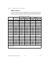
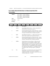
Appendix b register-level programming — programming pci-dio-96/pxi-6508/pci-6503 user manual b-18 ni.Com mode 0—basic i/o use mode 0 for simple i/o functions (no handshaking) for each of the three ports and assign each port as an input or an output port. Table b-4 shows the 16 possible i/o configura...
Page 60
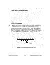
Appendix b register-level programming — programming © national instruments corporation b-19 pci-dio-96/pxi-6508/pci-6503 user manual mode 0 basic i/o programming example the following example shows how to configure ppi a for mode 0 input and output. Write (8255cnfg,0x80) set mode 0—ports a, b, and c...
Page 61
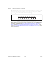
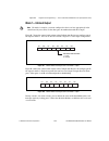
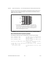
Appendix b register-level programming — programming pci-dio-96/pxi-6508/pci-6503 user manual b-20 ni.Com figure b-5 shows the control word written to the configuration register to configure port b for input in mode 1. Notice that port b does not have extra input or output lines left from port c when...
Page 62
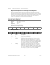
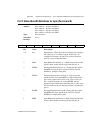
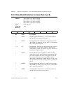
Appendix b register-level programming — port c status-word bit definitions for input (ports a and b) © national instruments corporation b-21 pci-dio-96/pxi-6508/pci-6503 user manual port c status-word bit definitions for input (ports a and b) address: base address + 02 (hex) for ppi a base address +...
Page 63
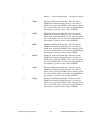
Appendix b register-level programming — port c status-word bit definitions for input (ports a and b) pci-dio-96/pxi-6508/pci-6503 user manual b-22 ni.Com 0 intrb interrupt request status for port b—interrupt request status for port b. This status flag, which operates only when intea is high, indicat...
Page 64
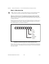
Appendix b register-level programming — port c status-word bit definitions for input (ports a and b) © national instruments corporation b-23 pci-dio-96/pxi-6508/pci-6503 user manual mode 1—strobed output note for mode 1 examples, you must configure the don’t care bits appropriately in the control wo...
Page 65
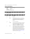
Appendix b register-level programming — port c status-word bit definitions for output (ports a and b) pci-dio-96/pxi-6508/pci-6503 user manual b-24 ni.Com port c status-word bit definitions for output (ports a and b) address: base address + 02 (hex) for ppi a base address + 06 (hex) for ppi b base a...
Page 66
Appendix b register-level programming — port c status-word bit definitions for output (ports a and b) © national instruments corporation b-25 pci-dio-96/pxi-6508/pci-6503 user manual 0 intrb interrupt request status for port b—this status flag, which operates only when intea is high, indicates that ...
Page 67
Appendix b register-level programming — port c status-word bit definitions for output (ports a and b) pci-dio-96/pxi-6508/pci-6503 user manual b-26 ni.Com mode 2—bidirectional bus note for mode 2 examples, you must configure the don’t care bits appropriately in the control word if you want to use th...
Page 68
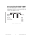
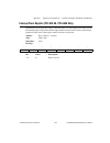
Appendix b register-level programming — port c status-word bit definitions for bidirectional data path (port a only) © national instruments corporation b-27 pci-dio-96/pxi-6508/pci-6503 user manual port c status-word bit definitions for bidirectional data path (port a only) address: base address + 0...
Page 69
Appendix b register-level programming — port c status-word bit definitions for bidirectional data path (port a only) pci-dio-96/pxi-6508/pci-6503 user manual b-28 ni.Com figure b-11 shows the port c pin assignments on the digital i/o connector when port c is configured for mode 2. Notice that the po...
Page 70
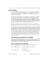
Appendix b register-level programming — port c status-word bit definitions for bidirectional data path (port a only) © national instruments corporation b-29 pci-dio-96/pxi-6508/pci-6503 user manual interrupt handling you must set the inten bit of interrupt control register 2 to enable interrupts. Cl...
Page 71
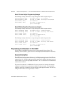
Appendix b register-level programming — port c status-word bit definitions for bidirectional data path (port a only) pci-dio-96/pxi-6508/pci-6503 user manual b-30 ni.Com mode 1 strobed output programming example the following example shows how to set up interrupts for mode 1 output for port a. Write...
Page 72
Appendix b register-level programming — port c status-word bit definitions for bidirectional data path (port a only) © national instruments corporation b-31 pci-dio-96/pxi-6508/pci-6503 user manual to determine the time between pulses generated by counter 0, multiply the load value by 500 ns (1/(2 m...
Page 73: Technical Support and
© national instruments corporation c-1 pci-dio-96/pxi-6508/pci-6503 user manual c technical support and professional services visit the following sections of the award-winning national instruments web site at ni.Com for technical support and professional services: • support —technical support at ni....
Page 74
Appendix c technical support and professional services pci-dio-96/pxi-6508/pci-6503 user manual c-2 ni.Com • declaration of conformity (doc) —a doc is our claim of compliance with the council of the european communities using the manufacturer’s declaration of conformity. This system affords the user...
Page 75: Glossary
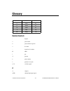
© national instruments corporation g-1 pci-dio-96/pxi-6508/pci-6503 user manual glossary symbol prefix value n nano 10 –9 μ micro 10 – 6 m milli 10 –3 k kilo 10 3 m mega 10 6 numbers/symbols ° degrees > greater than ≥ greater than or equal to less than – negative of, or minus Ω ohms / per % percent ...
Page 76
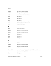
Glossary pci-dio-96/pxi-6508/pci-6503 user manual g-2 ni.Com airq0 ppi a port a interrupt enable bit airq1 ppi a port b interrupt enable bit ansi american national standards institute apa ppi a port a apb ppi a port b apc ppi a port c asic application specific integrated circuit awg american wire ga...
Page 77
Glossary © national instruments corporation g-3 pci-dio-96/pxi-6508/pci-6503 user manual cpb ppi c port b cpc ppi c port c ctr1 counter select bit ctrirq counter interrupt enable bit d daq a system that uses the personal computer to collect, measure, and generate electrical signals di digital input ...
Page 78
Glossary pci-dio-96/pxi-6508/pci-6503 user manual g-4 ni.Com h hex hexadecimal i i/o input/output ibf input buffer full signal in. Inches inte1 port a output interrupt enable bit inte2 port a input interrupt enable bit intea port a interrupt enable bit inteb port b interrupt enable bit inten interru...
Page 79
Glossary © national instruments corporation g-5 pci-dio-96/pxi-6508/pci-6503 user manual min minimum msb most significant bit o obf* output buffer full signal p pa, pb, pc port a, b, or c 0 through 7 lines pci peripheral component interconnect—a high-performance expansion bus architecture originally...
Page 80
Glossary pci-dio-96/pxi-6508/pci-6503 user manual g-6 ni.Com signal conditioning the manipulation of signals to prepare them for digitizing stb strobe input signal t ttl transistor-transistor logic typ typical v v volts v cc supply voltage; for example, the voltage a computer supplies to its plug-in...
Page 81: Index
© national instruments corporation i-1 pci-dio-96/pxi-6508/pci-6503 user manual index symbols +5 v supply pin connecting directly to the ground or other voltage source (caution), 3-10 pci-6503 (table), 3-7 pci-dio-96 and pxi-6508 (table), 3-4 numerics 82c53 programmable interval timer theory of oper...
Page 82
Index pci-dio-96/pxi-6508/pci-6503 user manual i-2 ni.Com cirq0, b-11 cirq1, b-11 ctr1, b-12 ctrirq, b-12 dirq0, b-10 dirq1, b-10 inten, b-12 mode 1 strobed input i/o, b-21 ibfa, b-21 ibfb, b-21 intea, b-21 inteb, b-21 intra, b-21 intrb, b-22 mode 1 strobed output i/o, b-24 intea, b-24 inteb, b-24 i...
Page 83
Index © national instruments corporation i-3 pci-dio-96/pxi-6508/pci-6503 user manual digital logic levels input signals, a-1 output signals, a-2 digital logic levels specifications, a-1 dirq0 bit description, b-10 dirq1 bit description, b-10 documentation ni resources, c-1 related documentation, x ...
Page 84
Index pci-dio-96/pxi-6508/pci-6503 user manual i-4 ni.Com inteb bit mode 1 strobed input description, b-21 mode 1 strobed output description, b-24 inten bit description, b-12 interface circuitry, pci, 4-3 interrupt control circuitry block diagram (figure), b-3 theory of operation, b-2 interrupt cont...
Page 85
Index © national instruments corporation i-5 pci-dio-96/pxi-6508/pci-6503 user manual port c status-word bit definitions, b-27 programming example, b-28 n national instruments support and services, c-1 ni support and services, c-1 o obf* signal description (table), 4-4 obfa* bit mode 1 strobed outpu...
Page 86
Index pci-dio-96/pxi-6508/pci-6503 user manual i-6 ni.Com inteb, b-24 intra, b-24 intrb, b-25 obfa*, b-24 obfb*, b-24 mode 2 bidirectional bus i/o, b-27 ibfa, b-27 inte1, b-27 inte2, b-27 intra, b-27 obfa*, b-27 power connections, 3-10 power requirement specifications, a-3 power-up state selection. ...
Page 87
Index © national instruments corporation i-7 pci-dio-96/pxi-6508/pci-6503 user manual port c pin assignments on i/o connector (figure), b-28 port c status-word bit definitions, b-27 programming example, b-28 pci initialization, b-15 pci local bus, b-14 programming examples, b-14 registers 82c53 regi...
Page 88
Index pci-dio-96/pxi-6508/pci-6503 user manual i-8 ni.Com timing specifications, 4-4 mode 1 input timing, 4-5 mode 1 output timing, 4-6 mode 2 bidirectional timing, 4-7 signal names used in timing diagrams (table), 4-4 training and certification (ni resources), c-1 transfer rates specifications, a-3...

