- DL manuals
- National Semiconductor
- Motherboard
- ADC081C021
- User Manual
National Semiconductor ADC081C021 User Manual
NOTE: The Evaluation Board is shipped with the Alert Option of the ADC. To
evaluate the Address Option, please order samples from
www.national.com
.
National Semiconductor
January 3, 2008
Rev – 1.1/CC
RoHS Compliant
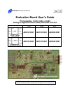
Evaluation Board User's Guide
I
2
C-Compatible, 12-Bit, 10-Bit, or 8-Bit
Analog-to-Digital Converter (ADC) with Alert Function
12-bit 10-bit 8-bit
ALERT Option
ADC121C021
ADC101C021
ADC081C021
ADDRESS Option
ADC121C027
ADC101C027
ADC081C027
Summary of ADC081C021
Page 1
Note: the evaluation board is shipped with the alert option of the adc. To evaluate the address option, please order samples from www.National.Com . National semiconductor january 3, 2008 rev – 1.1/cc rohs compliant evaluation board user's guide i 2 c-compatible, 12-bit, 10-bit, or 8-bit analog-to-d...
Page 2
Http://www.National.Com 2 table of contents 1.0 introduction ............................................................................................................................3 2.0 board assembly .................................................................................................
Page 3
Http://www.National.Com 3 1.0 introduction this design kit (consisting of the adc evaluation board and this user's guide) is designed to ease evaluation and design-in of national semiconductor’s adc121c021 family of analog- to-digital converters. The adcs can operate at speeds up to 188.9 ksps. The ...
Page 4
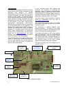
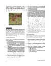
Http://www.National.Com 4 2.0 board assembly the adc121c02xeb evaluation board comes fully assembled and ready for use. The provided jumpers are in their recommended locations and suit the needs of most users. Refer to the bill of materials for a description of components, to figure 1 for major comp...
Page 5
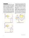
Http://www.National.Com 5 the lm4050-4.1 precision, micropower, shunt voltage reference is included on the adc121c02xeb as a clean reference solution for the adc. To evaluate the adc using the lm4050, simply short pins 1 & 2 of jp7, and move the va_select jumper to pins 7 & 8 of jp5 (figure 5). Figu...
Page 6
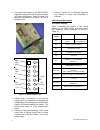
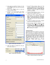
Http://www.National.Com 6 4. Connect the j1 header on the adc121c021 evaluation board to the wv4 serial connector (j7) on the wv4 board. Refer to figure 6 for the serial connection and figure 7 for the j1 header pin out. Figure 6: wv4 to adc121c02xeb connection figure 7: j1 (wv4s) header pin out 5. ...
Page 7
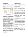
Http://www.National.Com 7 4.2 analog input signal there are three basic options for connecting an input signal to the adc. The three options facilitate ac-coupled and dc-coupled input signals. The first way to apply an input signal to the adc is to connect it to pin 2 of jp1. The signal’s return (gn...
Page 8
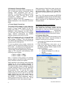
Http://www.National.Com 8 figure 9: system settings window 4.6 automatic conversion mode the automatic conversion mode configures the adc to continually perform conversions without receiving “read” instructions from the i 2 c controller. It is activated by writing a non-zero value into the cycle tim...
Page 9
Http://www.National.Com 9 3. Apply power as specified in section 4.4, click on the "reset" button and await the firmware to download. 4. Click on the "close" button to close the system settings window. 5. Navigate to the adc121c021 eval board window. This is the control panel for the device (figure ...
Page 10
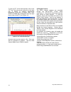
Http://www.National.Com 10 to view an fft of the data captured, click on the ‘fft’ tab. This plot may be zoomed in on the data plot. A display of dynamic performance parameters in the form of sinad, snr, thd, sfdr and enob will be displayed at the top right hand corner of the fft plot (figure 13). F...
Page 11
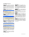
Http://www.National.Com 11 5.4 troubleshooting wavevision 5.4.1 problems problem 1: the “adc121c021 eval board” control panel appears briefly, but disappears after powering on the wavevision board. Try solutions a, b, and c. After trying these solutions, the wavevision system must be hard reset to r...
Page 12
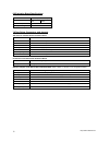
Http://www.National.Com 12 6.0 evaluation board specifications board size: 3.1" x 1.85" (7.9 cm x 4.6 cm) power requirements: min: +2.7v, 10ma max: +5.5v, 13ma i2c interface speed: 100 khz, 400khz, or 3.4 mhz analog input range: gnd to v a 7.0 test points, connectors, and jumpers test points on the ...
Page 13
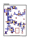
Http://www.National.Com 13 8.0 hardware schematic figure 10: adc121c021 evaluation board schematic sc l _ eep r o m s d a_ eep r o m sc l sd a r5 0 1 1 via 8 1 1 tp 8 ag n d 1 1 via 9 c1 1 ns va 1 gnd 2 vi n 3 a l r /adr 4 sc l 5 sd a 6 u1 a d c1 21 c0 21 r1 3 ns l2 100 uh 1 1 via 2 r4 ns vdd 14 gnd...
Page 14
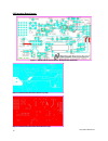
Http://www.National.Com 14 9.0 evaluation board layers figure 11: adc121c021 evaluation board: all layers with silk screen figure 12: adc121c021 evaluation board: top layer figure 13: adc121c021 evaluation board: bottom layer.
Page 15
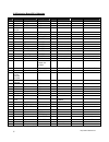
Http://www.National.Com 15 10.0 evaluation board bill of materials qty reference value description source source part # manufacturer manufacturer part # 1 c1 0 ohm r 0 ohm res 1 c2 470pf cap 2 c3,c7 10.0uf cap digikey 511-1463-1-nd kemet 5 c4,c5, c8,c12 0.1uf cap 1 c6,c11 ns cap 1 c9 1.0uf cap 1 c10...
Page 16
Http://www.National.Com 16 by using this product, you are agreeing to be bound by the terms and conditions of national semiconductor's end user license agreement. Do not use this product until you have read and agreed to the terms and conditions of that agreement. If you do not agree with them, cont...
Page 17
Evaluation board/kit/module (evm) additional terms texas instruments (ti) provides the enclosed evaluation board/kit/module (evm) under the following conditions: the user assumes all responsibility and liability for proper and safe handling of the goods. Further, the user indemnifies ti from all cla...
Page 18
Fcc interference statement for class b evm devices this equipment has been tested and found to comply with the limits for a class b digital device, pursuant to part 15 of the fcc rules. These limits are designed to provide reasonable protection against harmful interference in a residential installat...
Page 19
【 【 important notice for users of this product in japan】 】 this development kit is not certified as confirming to technical regulations of radio law of japan if you use this product in japan, you are required by radio law of japan to follow the instructions below with respect to this product: 1. Use...
Page 20
Evaluation board/kit/module (evm) warnings, restrictions and disclaimers for feasibility evaluation only, in laboratory/development environments. Unless otherwise indicated, this evm is not a finished electrical equipment and not intended for consumer use. It is intended solely for use for prelimina...
Page 21
Important notice texas instruments incorporated and its subsidiaries (ti) reserve the right to make corrections, enhancements, improvements and other changes to its semiconductor products and services per jesd46, latest issue, and to discontinue any product or service per jesd48, latest issue. Buyer...

